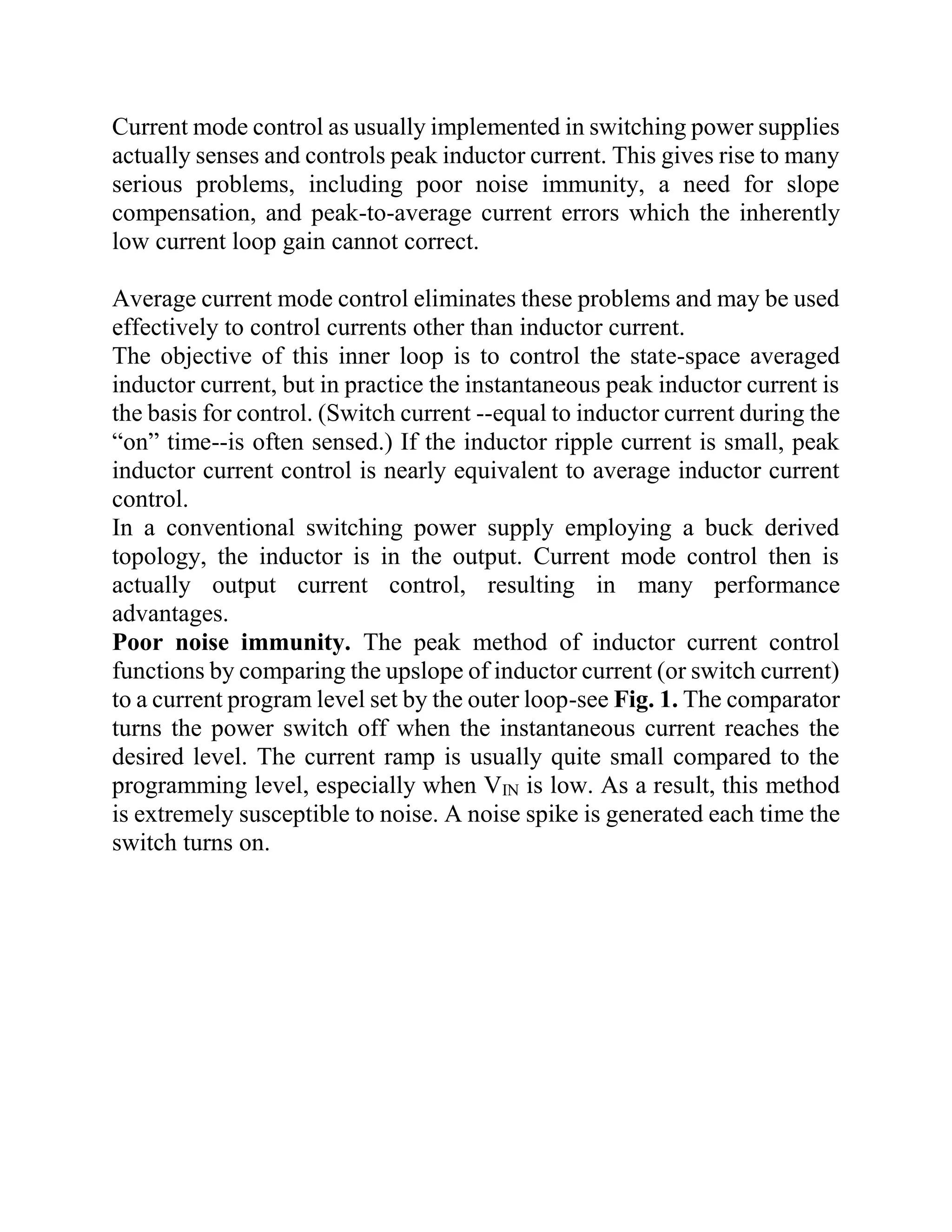
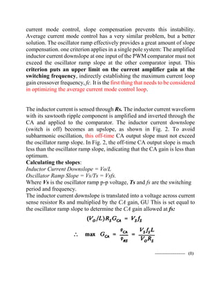
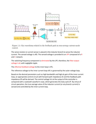
The document discusses average current mode control (ACMC) in switching power supplies. It describes how ACMC improves upon peak current mode control by introducing a high-gain integrating current error amplifier into the current loop. This allows the average current to track the desired program level more accurately and provides better noise immunity, stability without slope compensation, and ability to control currents in any circuit branch. The document also discusses various ACMC circuit implementations and their advantages, including true average current control using a low-pass filter to isolate the average current value.
![Pole RF, CFP CFz/(CFP+ CFz) is set at switching frequency fs (100 kHz). This pole has one
purpose-to eliminate noise spikes riding on the current waveform.
Discontinuous Operation. When the load current I, becomes small, the inductor current
becomes discontinuous. The current level at the continuous/discontinuous mode boundary is:
In the discontinuous mode, below the mode boundary, changes in I, require large duty cycle
changes. But with average current mode control, the high gain of the current error amplifier
provides the large duty cycle changes necessary to accommodate changes in load current,
thereby maintaining good average current regulation. when the current loop is closed, the voltage
across current sense resistor VRS equals the current programming voltage VCA (from the voltage
error amplifier) at frequencies below fs. The transconductance of the closed current loop is a part
of the outer voltage control loop:
The closed loop transconductance rolls off and assumes a single pole characteristic at the open
loop crossover frequency, fs. [1]
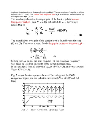
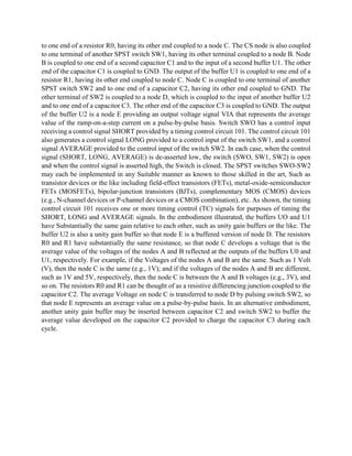
True Average Circuit with Control Loops.](https://image.slidesharecdn.com/averaging-1-221121154552-b9ffde3f/85/Averaging-1-docx-6-320.jpg)
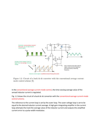
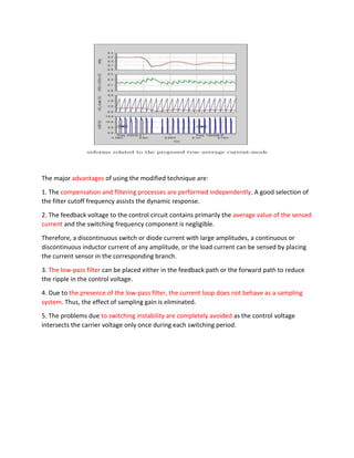
![Average Current mode control (ACM Circuit 3): as usually implemented in switching power
supplies actually senses and controls peak inductor current.
This gives rise to many serious problems, including poor noise immunity, a need for slope
compensation, and peak-to-average current mirror which the inherently low current loop gain
cannot collect.
ACM control eliminates these problems and may be used effectively to control currents other
than inductor current, allowing a much broader range of topological application. [TI_avg]
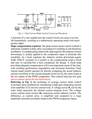
Fig. 2, the technique of ACM control overcomes these problems by introducing a high gain
integrating current error amplifier (CA) into the current loop.
A voltage across Rp (set by the outer loop) represents the desired current program level.
The voltage across current sense resistor Rs represents actual inductor current.
The current error, is amplified and compared to a large amplitude sawtooth (oscillator ramp) at
the PWM comparator inputs.
The gain-bandwidth characteristic of the current loop can be tailored for optimum performance
by the compensation network around the CA.
Compared with peak current mode control, the current loop gain crossover frequency, Ie, can be
made approximately the same, but the gain will be much greater at lower frequencies.
The result is: 1) Average current tracks the current program with a high degree of accuracy.
This is especially important in high power factor preregulators, enabling less than 3% harmonic
distortion to be achieved with a relatively small inductor.
In fact, average current mode control functions well even when the mode boundary is crossed
into the discontinuous mode at low current levels. The outer voltage control loop is oblivious to
this mode change.](https://image.slidesharecdn.com/averaging-1-221121154552-b9ffde3f/85/Averaging-1-docx-11-320.jpg)


![11.[49 61]optimizing the output current for a dc-dc converter](https://cdn.slidesharecdn.com/ss_thumbnails/11-49-61optimizingtheoutputcurrentforadc-dcconverter-120512235916-phpapp01-thumbnail.jpg?width=640&height=640&fit=bounds)


