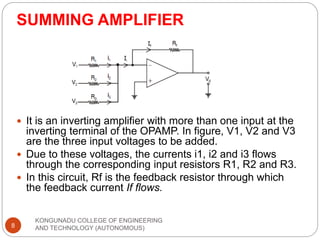
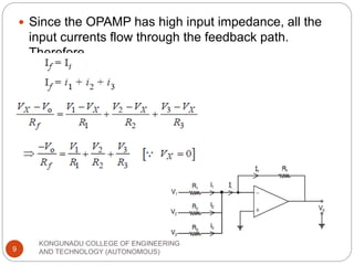
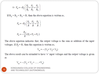
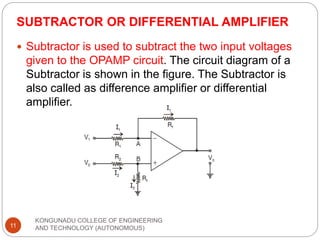
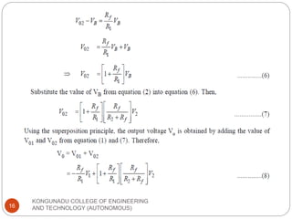
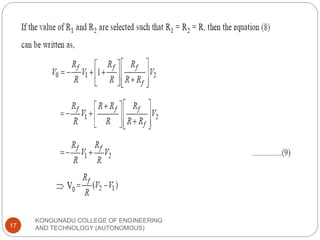
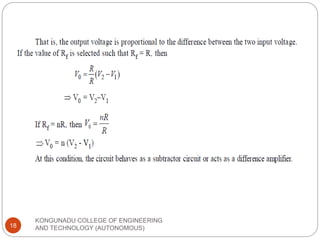
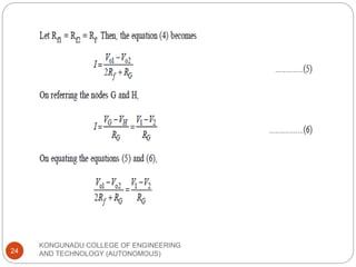
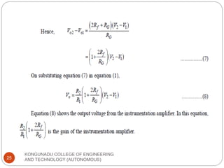
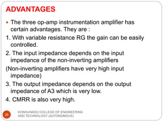
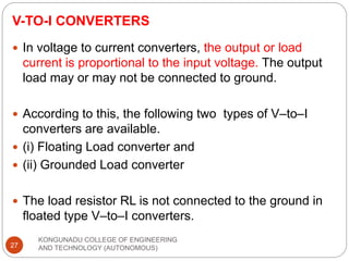
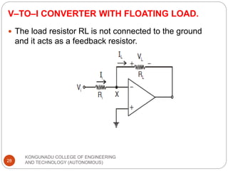
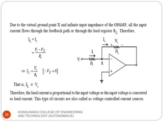
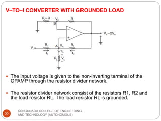
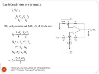
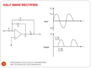
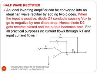
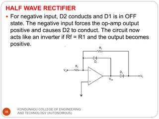
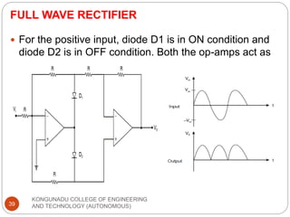
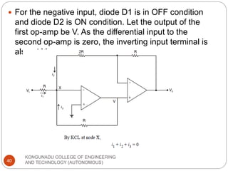
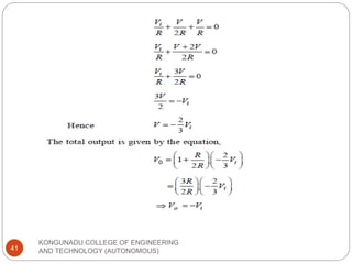
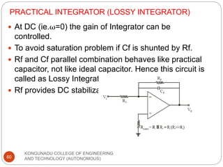
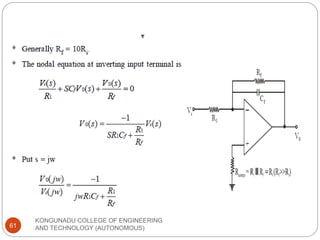
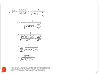
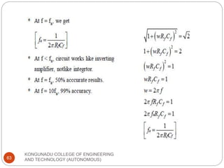
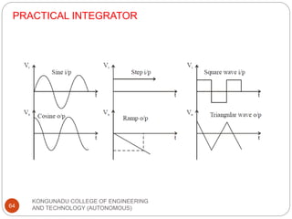
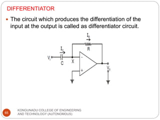
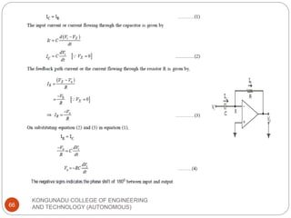
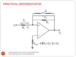
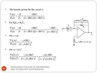
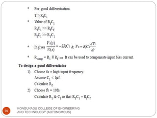
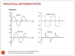
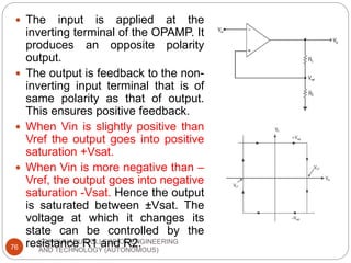
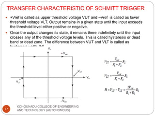
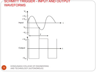
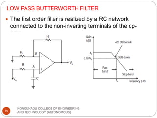
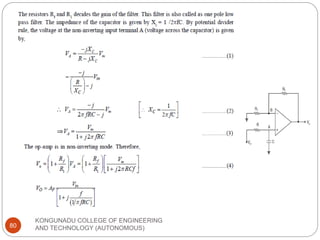
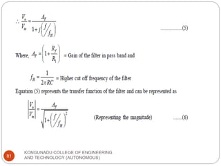
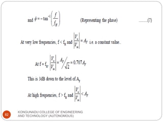
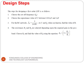
The document discusses various applications of operational amplifiers including scale changers, summing amplifiers, subtractors, instrumentation amplifiers, voltage to current and current to voltage converters, precision rectifiers, peak detectors, clippers, clampers, and filters. It provides circuit diagrams and explanations of how each application circuit works using operational amplifiers. The applications can be classified as linear applications like adders and non-linear applications like rectifiers.
Block diagram of a typical op-amp – characteristics of ideal and practical op-amp - parameters of opamp – inverting and non-inverting amplifier configurations - frequency response - circuit stability.
This paper describes about different types of voltage followers. Each follower has its own advantages and limitations. The voltage follower can be characterized with current mirror source current or it can be used as a ideal current source. Voltage Follower is one of the most important analog circuits required in many analog integrated circuits. Input impedance of op amp is very high, giving effective isolation of the output from the signal source.
Students, digital devices and success - Andreas Schleicher - 27 May 2024..pptxEduSkills OECD
Andreas Schleicher presents at the OECD webinar ‘Digital devices in schools: detrimental distraction or secret to success?’ on 27 May 2024. The presentation was based on findings from PISA 2022 results and the webinar helped launch the PISA in Focus ‘Managing screen time: How to protect and equip students against distraction’ https://www.oecd-ilibrary.org/education/managing-screen-time_7c225af4-en and the OECD Education Policy Perspective ‘Students, digital devices and success’ can be found here - https://oe.cd/il/5yV
Operation “Blue Star” is the only event in the history of Independent India where the state went into war with its own people. Even after about 40 years it is not clear if it was culmination of states anger over people of the region, a political game of power or start of dictatorial chapter in the democratic setup.
The people of Punjab felt alienated from main stream due to denial of their just demands during a long democratic struggle since independence. As it happen all over the word, it led to militant struggle with great loss of lives of military, police and civilian personnel. Killing of Indira Gandhi and massacre of innocent Sikhs in Delhi and other India cities was also associated with this movement.
How to Split Bills in the Odoo 17 POS ModuleCeline George
Bills have a main role in point of sale procedure. It will help to track sales, handling payments and giving receipts to customers. Bill splitting also has an important role in POS. For example, If some friends come together for dinner and if they want to divide the bill then it is possible by POS bill splitting. This slide will show how to split bills in odoo 17 POS.
How to Make a Field invisible in Odoo 17Celine George
It is possible to hide or invisible some fields in odoo. Commonly using “invisible” attribute in the field definition to invisible the fields. This slide will show how to make a field invisible in odoo 17.
Unit 8 - Information and Communication Technology (Paper I).pdfThiyagu K
This slides describes the basic concepts of ICT, basics of Email, Emerging Technology and Digital Initiatives in Education. This presentations aligns with the UGC Paper I syllabus.
How to Create Map Views in the Odoo 17 ERPCeline George
The map views are useful for providing a geographical representation of data. They allow users to visualize and analyze the data in a more intuitive manner.
The Indian economy is classified into different sectors to simplify the analysis and understanding of economic activities. For Class 10, it's essential to grasp the sectors of the Indian economy, understand their characteristics, and recognize their importance. This guide will provide detailed notes on the Sectors of the Indian Economy Class 10, using specific long-tail keywords to enhance comprehension.
For more information, visit-www.vavaclasses.com
We all have good and bad thoughts from time to time and situation to situation. We are bombarded daily with spiraling thoughts(both negative and positive) creating all-consuming feel , making us difficult to manage with associated suffering. Good thoughts are like our Mob Signal (Positive thought) amidst noise(negative thought) in the atmosphere. Negative thoughts like noise outweigh positive thoughts. These thoughts often create unwanted confusion, trouble, stress and frustration in our mind as well as chaos in our physical world. Negative thoughts are also known as “distorted thinking”.
This is a presentation by Dada Robert in a Your Skill Boost masterclass organised by the Excellence Foundation for South Sudan (EFSS) on Saturday, the 25th and Sunday, the 26th of May 2024.
He discussed the concept of quality improvement, emphasizing its applicability to various aspects of life, including personal, project, and program improvements. He defined quality as doing the right thing at the right time in the right way to achieve the best possible results and discussed the concept of the "gap" between what we know and what we do, and how this gap represents the areas we need to improve. He explained the scientific approach to quality improvement, which involves systematic performance analysis, testing and learning, and implementing change ideas. He also highlighted the importance of client focus and a team approach to quality improvement.
The Art Pastor's Guide to Sabbath | Steve ThomasonSteve Thomason
What is the purpose of the Sabbath Law in the Torah. It is interesting to compare how the context of the law shifts from Exodus to Deuteronomy. Who gets to rest, and why?
The Art Pastor's Guide to Sabbath | Steve Thomason
LIC UNIT II.pptx
1. UNIT – II
APPLICATIONS OF OPERATIONAL
AMPLIFIERS
LINEAR INTEGRATED CIRCUITS
1
KONGUNADU COLLEGE OF ENGINEERING
AND TECHNOLOGY (AUTONOMOUS)
2. APPLICATIONS OF OPERATIONAL
AMPLIFIERS
Syllabus
Basic Op-amp Applications - Scale Changer -
Summing Amplifier – Subtractor - Instrumentation
amplifier - V-to-I and I-to-V converters – Precision
Rectifier – Peak detector - Clipper and Clamper -
Sample and Hold circuit - Log amplifier - Antilog
amplifier - Differentiator -- Integrator - Comparators –
Schmitt trigger – Low pass – high pass and band
pass butterworth filters.
2
KONGUNADU COLLEGE OF ENGINEERING
AND TECHNOLOGY (AUTONOMOUS)
3. BASIC OP-AMP APPLICATIONS
KONGUNADU COLLEGE OF ENGINEERING
AND TECHNOLOGY (AUTONOMOUS)
3
Operational amplifiers have more number of applications
and they forms the basic building block of many linear and
non-linear analog systems.
Sign changer, adder, Subtractor, voltage follower and
instrumentation amplifier are some of the linear
applications of the operational amplifiers.
Rectifier, peak detector, clipper and clamper, logarithmic
amplifier and anti-logarithmic amplifier are some of the
non-linear analog applications of the operational amplifier.
Operational amplifiers (OPAMP) are high gain direct-
coupled amplifiers and used to perform many
mathematical operations. Ideal OPAMP's are having
infinite voltage gain and infinite input impedance with zero
output impedance.
5. KONGUNADU COLLEGE OF ENGINEERING
AND TECHNOLOGY (AUTONOMOUS)
5
The above result indicates that, input voltage is zero. If
there is a short circuit between the two input terminal, then
the input voltage Vi becomes zero. But there exist no real
short circuit between the two input terminals. That is, there
exist a virtual short circuit across the input terminals of an
OPAMP.
Since one of the input terminal is grounded, the
virtual short becomes virtual ground and voltages at
the point X is zero (VX = 0). That is, the point X is at
virtual ground.
6. SCALE CHANGER
KONGUNADU COLLEGE OF ENGINEERING
AND TECHNOLOGY (AUTONOMOUS)
6
Scale changer is a circuit in which the output voltage is
equal to the input voltage multiplied by a constant scale. If
Vi is the input voltage and ‘K’ is the Scale factor, then the
output voltage Vo is equal to KVi
8. SUMMING AMPLIFIER
KONGUNADU COLLEGE OF ENGINEERING
AND TECHNOLOGY (AUTONOMOUS)
8
It is an inverting amplifier with more than one input at the
inverting terminal of the OPAMP. In figure, V1, V2 and V3
are the three input voltages to be added.
Due to these voltages, the currents i1, i2 and i3 flows
through the corresponding input resistors R1, R2 and R3.
In this circuit, Rf is the feedback resistor through which
the feedback current If flows.
9. KONGUNADU COLLEGE OF ENGINEERING
AND TECHNOLOGY (AUTONOMOUS)
9
Since the OPAMP has high input impedance, all the
input currents flow through the feedback path.
Therefore,
11. SUBTRACTOR OR DIFFERENTIAL AMPLIFIER
KONGUNADU COLLEGE OF ENGINEERING
AND TECHNOLOGY (AUTONOMOUS)
11
Subtractor is used to subtract the two input voltages
given to the OPAMP circuit. The circuit diagram of a
Subtractor is shown in the figure. The Subtractor is
also called as difference amplifier or differential
amplifier.
12. KONGUNADU COLLEGE OF ENGINEERING
AND TECHNOLOGY (AUTONOMOUS)
12
V1 and V2 are the inputs given to the Subtractor and
Vo is its output. R1 and R2 are the input resistor
connected to the inverting and non-inverting
terminals of the OPAMP.
To find the output, superposition principle has to be
applied by considering one input at a time.
13. KONGUNADU COLLEGE OF ENGINEERING
AND TECHNOLOGY (AUTONOMOUS)
13
Case (i) :
First consider that, only the input V1 is given to the
circuit and V2 is made as zero. Now, the circuit
diagram is changed as shown in figure.
14. KONGUNADU COLLEGE OF ENGINEERING
AND TECHNOLOGY (AUTONOMOUS)
14
Case (ii) :
Next, the input V2 is given to the circuit and V1 is
made as zero. The circuit diagram for this case is
shown in figure
19. INSTRUMENTATION AMPLIFIER
KONGUNADU COLLEGE OF ENGINEERING
AND TECHNOLOGY (AUTONOMOUS)
19
The necessary demand of the industry is to measure
and control many physical quantities. Some typical
examples are measurement and control of
temperature, humidity, flow etc. Transducers are
usually used to measure all these, low output
voltages. This low voltage has to be amplified so as
to drive the indicator or display. An instrumentation
amplifier does this. Such an amplifier is an integral
part of modern testing and measurement
instrumentation.
20. INSTRUMENTATION AMPLIFIER
KONGUNADU COLLEGE OF ENGINEERING
AND TECHNOLOGY (AUTONOMOUS)
20
A good instrumentation amplifier has to meet the following
requirements.
1. Finite, accurate and stable gain
2. Easy gain adjustment
3. High input and low input impedances
4. High CMRR
5. Low power consumption
6. High slew rate
7. Low thermal and time drifts
8. Low dc offset
There are specially designed OPAMP’s such as A 725 that
satisfies the above requirements.
AD 521, AD524, AD620, LM 363, are some of the commercially
available chips.
22. ANALYSIS OF THREE OPAMP INSTRUMENTATION
AMPLIFIER
KONGUNADU COLLEGE OF ENGINEERING
AND TECHNOLOGY (AUTONOMOUS)
22
The instrumentation amplifier has a basic difference
amplifier at the output stage. If the output of the op-
amp A1 is Vo1 and that of A2 is Vo2 then,
26. ADVANTAGES
KONGUNADU COLLEGE OF ENGINEERING
AND TECHNOLOGY (AUTONOMOUS)
26
The three op-amp instrumentation amplifier has
certain advantages. They are :
1. With variable resistance RG the gain can be easily
controlled.
2. The input impedance depends on the input
impedance of the non-inverting amplifiers
(Non-inverting amplifiers have very high input
impedance)
3. The output impedance depends on the output
impedance of A3 which is very low.
4. CMRR is also very high.
27. V-TO-I CONVERTERS
KONGUNADU COLLEGE OF ENGINEERING
AND TECHNOLOGY (AUTONOMOUS)
27
In voltage to current converters, the output or load
current is proportional to the input voltage. The output
load may or may not be connected to ground.
According to this, the following two types of V–to–I
converters are available.
(i) Floating Load converter and
(ii) Grounded Load converter
The load resistor RL is not connected to the ground in
floated type V–to–I converters.
28. V–TO–I CONVERTER WITH FLOATING LOAD.
KONGUNADU COLLEGE OF ENGINEERING
AND TECHNOLOGY (AUTONOMOUS)
28
The load resistor RL is not connected to the ground
and it acts as a feedback resistor.
30. V–TO–I CONVERTER WITH GROUNDED LOAD
KONGUNADU COLLEGE OF ENGINEERING
AND TECHNOLOGY (AUTONOMOUS)
30
The input voltage is given to the non-inverting terminal of the
OPAMP through the resistor divider network.
The resistor divider network consist of the resistors R1, R2 and
the load resistor RL. The load resistor RL is grounded.
33. CURRENT TO VOLTAGE (I–TO–V) CONVERTER
KONGUNADU COLLEGE OF ENGINEERING
AND TECHNOLOGY (AUTONOMOUS)
33
In current to voltage converter, the output voltage is
proportional to the input current.
In this circuit, the input current is given to the inverting
terminal of the OPAMP and in the feedback, a resistor
R is connected.
35. PRECISION RECTIFIER
KONGUNADU COLLEGE OF ENGINEERING
AND TECHNOLOGY (AUTONOMOUS)
35
Rectifiers are circuits used to convert ac signal into dc
signal. Normally diodes are used for rectification purpose.
The major demerit of using diode is that it cannot rectify
voltages below 0.7V, the cut in voltage for a diode. Due to
this, the conventional rectifiers produce distortion at the
output.
To achieve precision rectification, a circuit is needed which
keeps output equal to input for input greater than zero. This
is done by using OPAMP along with diodes and these
circuits are called as Precision rectifiers.
They rectify voltages below 0.7V also, hence called small
signal precision rectifiers. The precision rectifiers are
classified as Half wave and Full wave precision rectifiers.
37. HALF WAVE RECTIFIER
KONGUNADU COLLEGE OF ENGINEERING
AND TECHNOLOGY (AUTONOMOUS)
37
An ideal inverting amplifier can be converted into an
ideal half wave rectifier by adding two diodes. When
the input is positive, diode D1 conducts causing VOA to
go to negative by one diode drop. Hence diode D2
gets reverse biased and the output becomes zero. For
all practical purposes no current flows through R1 and
input current flows through D1 only.
38. HALF WAVE RECTIFIER
KONGUNADU COLLEGE OF ENGINEERING
AND TECHNOLOGY (AUTONOMOUS)
38
For negative input, D2 conducts and D1 is in OFF
state. The negative input forces the op-amp output
positive and causes D2 to conduct. The circuit now
acts like an inverter if Rf = R1 and the output becomes
positive.
39. FULL WAVE RECTIFIER
KONGUNADU COLLEGE OF ENGINEERING
AND TECHNOLOGY (AUTONOMOUS)
39
For the positive input, diode D1 is in ON condition and
diode D2 is in OFF condition. Both the op-amps act as
inverter and V0 = Vi.
40. KONGUNADU COLLEGE OF ENGINEERING
AND TECHNOLOGY (AUTONOMOUS)
40
For the negative input, diode D1 is in OFF condition
and diode D2 is ON condition. Let the output of the
first op-amp be V. As the differential input to the
second op-amp is zero, the inverting input terminal is
also at V.
42. PEAK DETECTORS
KONGUNADU COLLEGE OF ENGINEERING
AND TECHNOLOGY (AUTONOMOUS)
42
Square, triangular, saw tooth and pulse waves are non
sinusoidal waveforms. To measure the true rms value
of the signal, the peak values of those signals should
be known. This is achieved by using a peak detector.
It is a circuit that measures the positive peaks of the
input. The circuit follows the voltage peaks of a signal
and stores the highest value on a capacitor.
If a higher peak signal value comes along, then this
new value is stored. The highest value is stored until
the capacitor is discharged.
43. KONGUNADU COLLEGE OF ENGINEERING
AND TECHNOLOGY (AUTONOMOUS)
43
When the input voltage exceeds the voltage across the capacitor, the
diode is ON and the circuit acts like a voltage follower. Hence, the
output follows the input until the condition exists.
If the input is less than the voltage across the capacitor, the diode
becomes reverse biased. The capacitor holds the stored charge till the
input voltage again exceeds the voltage
across the capacitor.
44. KONGUNADU COLLEGE OF ENGINEERING
AND TECHNOLOGY (AUTONOMOUS)
44
At time ‘t1’ the signal peak is
recognized as V1. The peak at ‘t2’
cannot be recognized as the
voltage at the point V2 is less than
the previously occurred peak (V1)
in the input.
At time ‘t3’, the input signal has a
peak voltage of V3 and it is greater
than the voltage V1.
Therefore, V3 is recognized as
new peak of the input signal
The circuit can be reset or the
capacitor voltage can be made
zero by connecting a low leakage
MOSFET switch across the
capacitor.
Reversing the diode position
detects the lowest or most
negative voltage of the input
signal. Peak detectors are used in
test and measurement instruments
and in AM communication circuits..
45. CLIPPERS
KONGUNADU COLLEGE OF ENGINEERING
AND TECHNOLOGY (AUTONOMOUS)
45
The circuits used to clip off unwanted portions of the input
above or below certain level so as to give required output
are called as limiting circuits or clipper circuits.
They may be classified as Positive clipper and Negative
clippers. Positive Clippers remove some positive part of
the input whereas negative clippers remove some negative
part of the input.
47. KONGUNADU COLLEGE OF ENGINEERING
AND TECHNOLOGY (AUTONOMOUS)
47
The clipping level is
determined by the internal
setting of Vset obtained from
VCC or –VEE.
During the positive half cycle,
diode D conducts till the input
is equal to the reference
voltage.
When it becomes less than
the reference voltage, the op-
amp acts like a voltage
follower and V0 =Vin. As it
becomes greater, D get
reversed biased and the op-
amp goes to open loop.
Hence the op-amp goes into
positive saturation (+Vsat).
Now the output remains at
Vset and the entire waveform
above Vset gets clipped off.
48. CLAMPERS
KONGUNADU COLLEGE OF ENGINEERING
AND TECHNOLOGY (AUTONOMOUS)
48
Circuits that are used to add a d.c. level as per the
requirement to the a.c. output are called clamper circuits.
They are also called as dc restorer circuits. Clampers are
classified as positive clamper and negative clampers.
49. KONGUNADU COLLEGE OF ENGINEERING
AND TECHNOLOGY (AUTONOMOUS)
49
In this circuit, OPAMP is in
inverting mode. When the input
is negative, output goes
positive. This makes diode D to
ON state.
Now the capacitor charges to
the peak value of the negative
cycle of the input.
Beyond the negative input
peaks, the diode comes to OFF
state and stops conducting.
Thus, the output is the sum of
the input and capacitor voltage.
Let Vp be the voltage up to
which the capacitor gets
charged. Now the input
voltage is equal to (Vi + Vp).
Thus the d.c. voltage equal
to Vp gets added in the ac
output. The output is same
50. LOGARITHMIC AMPLIFIER
KONGUNADU COLLEGE OF ENGINEERING
AND TECHNOLOGY (AUTONOMOUS)
50
There are several applications of log and antilog amplifiers.
Antilog computations may require functions such as ln x,
log x, sinh x, etc. These are performed with log-antilog
amplifiers.
Log amplifiers can perform direct dB display on digital
voltmeter and spectrum analyzer.
Dynamic range of a signal can also be compressed by
using log-amplifiers.
53. ANTILOGARITHMIC AMPLIFIER
KONGUNADU COLLEGE OF ENGINEERING
AND TECHNOLOGY (AUTONOMOUS)
53
The positions of diode and resistor are interchanged
with respect to log amplifier.
55. KONGUNADU COLLEGE OF ENGINEERING
AND TECHNOLOGY (AUTONOMOUS)
55
The basic antilog amplifier can also be constructed by
replacing the diode with a transistor. The output is
proportional to the antilogarithm of the input and given
by the equation (5).
This equation is temperature dependent and the
antilog amplifier also suffers from the same problem
as that of log amplifier. Hence, some sort of
temperature compensation is required.
This antilog amplifier is subjected to noise, bias
currents, offset voltages, drifts and frequency stability
problems.
Transistorized circuits give accuracy, reduced bulk
resistance and high operating ranges.
56. INTEGRATOR
KONGUNADU COLLEGE OF ENGINEERING
AND TECHNOLOGY (AUTONOMOUS)
56
Integrator is a circuit in which the output voltage is
equal to the integration of input voltage.
It consists of a resistor R at the input path and a
capacitor C at the feedback path.
59. PRACTICAL INTEGRATOR
KONGUNADU COLLEGE OF ENGINEERING
AND TECHNOLOGY (AUTONOMOUS)
59
The input impedance of an ideal OPAMP is
infinity and no current flows through the
amplifier through its input terminal.
In practical amplifier, it is not the case and
some amount of current flows into the
amplifier. That is, the input transistor of an
OPAMP draws a small bias current.
This bias current charges the capacitor to
the maximum value and the output
becomes saturated. To prevent the
saturation of the capacitor, a large
resistance Rs in the order of 1MΩ is
connected across the capacitor.
This high valued resistance RS provides a
discharge path for the charges in C. This
resistance prevents the output from going
into full saturation condition. Since the
value of RS is very high, it will not affect the
normal performance of the integrator.
60. PRACTICAL INTEGRATOR (LOSSY INTEGRATOR)
KONGUNADU COLLEGE OF ENGINEERING
AND TECHNOLOGY (AUTONOMOUS)
60
At DC (ie.ω=0) the gain of Integrator can be
controlled.
To avoid saturation problem if Cf is shunted by Rf.
Rf and Cf parallel combination behaves like practical
capacitor, not like ideal capacitor. Hence this circuit is
called as Lossy Integrator.
Rf provides DC stabilization.
65. DIFFERENTIATOR
KONGUNADU COLLEGE OF ENGINEERING
AND TECHNOLOGY (AUTONOMOUS)
65
The circuit which produces the differentiation of the
input at the output is called as differentiator circuit.
71. COMPARATORS
KONGUNADU COLLEGE OF ENGINEERING
AND TECHNOLOGY (AUTONOMOUS)
71
Operational amplifiers in the open loop configuration
can be used as a comparator. Based on the input,
comparator produces the output that is either positive
saturation voltage or negative saturation voltage.
A comparator is a circuit that compares the signal
applied at one input with a known reference signal at
the other input and produce an output of +Vsat or –
Vsat. The output is non linear with respect to the input.
73. NON-INVERTING COMPARATOR
KONGUNADU COLLEGE OF ENGINEERING
AND TECHNOLOGY (AUTONOMOUS)
73
In this type of comparator, the input signal is applied to
the non-inverting terminal and no reference signal is
applied. The inverting input is at zero potential.
74. SCHMITT TRIGGER
KONGUNADU COLLEGE OF ENGINEERING
AND TECHNOLOGY (AUTONOMOUS)
74
Open loop is used in basic comparator circuits. As the gain
is large, even small noise voltages can cause false
triggering in comparators to change its state.
The comparator used to avoid such false triggering is
called as Schmitt trigger or Regenerative comparator. They
use positive feedback. Such positive feedback when added
to a comparator increases the gain. Hence the transfer
curve becomes closer to the ideal one.
In practical circuits it is not possible to maintain loop gain
to unity for a long time because of supply voltage and
temperature variations. Therefore, a gain value greater
than unity is chosen. This also gives an output virtually
discontinuous at the comparison voltage. This circuit
however now exhibits a phenomenon called Hysteresis or
Backlash.
76. KONGUNADU COLLEGE OF ENGINEERING
AND TECHNOLOGY (AUTONOMOUS)
76
The input is applied at the
inverting terminal of the OPAMP. It
produces an opposite polarity
output.
The output is feedback to the non-
inverting input terminal that is of
same polarity as that of output.
This ensures positive feedback.
When Vin is slightly positive than
Vref the output goes into positive
saturation +Vsat.
When Vin is more negative than –
Vref, the output goes into negative
saturation -Vsat. Hence the output
is saturated between ±Vsat. The
voltage at which it changes its
state can be controlled by the
resistance R1 and R2.
77. TRANSFER CHARACTERISTIC OF SCHMITT TRIGGER
KONGUNADU COLLEGE OF ENGINEERING
AND TECHNOLOGY (AUTONOMOUS)
77
+Vref is called as upper threshold voltage VUT and –Vref is called as lower
threshold voltage VLT. Output remains in a given state until the input exceeds
the threshold level either positive or negative.
Once the output changes its state, it remains there indefinitely until the input
crosses any of the threshold voltage levels. This is called hysteresis or dead
band or dead zone. The difference between VUT and VLT is called as
hysteresis width (H).
78. SCHMITT TRIGGER - INPUT AND OUTPUT
WAVEFORMS
KONGUNADU COLLEGE OF ENGINEERING
AND TECHNOLOGY (AUTONOMOUS)
78
79. LOW PASS BUTTERWORTH FILTER
KONGUNADU COLLEGE OF ENGINEERING
AND TECHNOLOGY (AUTONOMOUS)
79
The first order filter is realized by a RC network
connected to the non-inverting terminals of the op-
amp.
84. HIGH PASS BUTTERWORTH FILTER
KONGUNADU COLLEGE OF ENGINEERING
AND TECHNOLOGY (AUTONOMOUS)
84
A high pass circuit attenuates all the frequencies
lesser than the cut off frequency fL. This filter is
complementary to the LPF. This cut off frequency is
called as the lower cut off frequency.
85. KONGUNADU COLLEGE OF ENGINEERING
AND TECHNOLOGY (AUTONOMOUS)
85
All the frequencies greater than the lower cut off
frequency are passed. The simple RC network
attached to then on-inverting terminal is similar to that
of LPF but the positions of R
and C are interchanged. The circuit can be analyzed
for its cut off frequency. Voltage at the point A is given
by,
89. BAND PASS FILTERS
KONGUNADU COLLEGE OF ENGINEERING
AND TECHNOLOGY (AUTONOMOUS)
89
A band pass filter has pass band between two cut off
frequencies fH and fL such that fH is greater than fL. Any
frequency outside this pass band is rejected or
attenuated. This is a frequency selective filter.
The pass band which is between these two cut off
frequencies is called bandwidth of the filter (BW).
The frequency at the centre of the pass band is called
Centre frequency (fC) where the gain is maximum.
Practically it is not exactly at the centre and also called
as resonant frequency.
90. WIDE BAND PASS FILTER
KONGUNADU COLLEGE OF ENGINEERING
AND TECHNOLOGY (AUTONOMOUS)
90
92. WIDE BAND PASS FILTER
KONGUNADU COLLEGE OF ENGINEERING
AND TECHNOLOGY (AUTONOMOUS)
92
93. Narrow Band Pass Filter
KONGUNADU COLLEGE OF ENGINEERING
AND TECHNOLOGY (AUTONOMOUS)
93
A narrow band pass filter uses two feedback paths with
only one op-amp as against the two op-amp in wide band
filter. This filter is unique in the following respects :
1. It has two feedback paths, hence named multiple-
feedback filter.
2. The op-amp is used in inverting mode.
96. SAMPLE AND HOLD CIRCUITS
KONGUNADU COLLEGE OF ENGINEERING
AND TECHNOLOGY (AUTONOMOUS)
96
Analog voltage given as input to the analog to digital
converter should be held constant during the
conversion time period. It is necessary to have an
accurate A/D conversion. Otherwise, some variation
may be noticed in the output digital data.
If the analog input voltage is changed by more than an
amount of half-LSB value, then an error can be
occurred in the digital output code.
To avoid or minimize these errors, it is necessary to
hold the analog input value as constant during the
conversion period. To serve this purpose, sample and
hold circuits are used.
97. Principle of operation
KONGUNADU COLLEGE OF ENGINEERING
AND TECHNOLOGY (AUTONOMOUS)
97
The sample and hold circuit samples the analog input signal in response
to the sampling command and hold it at the output until the arrival of the
next command.
The sampling command is used to operate the sampling switch ‘S’. When
the switch ‘S’ is in the closed position, it connects the analog input signal
to the hold capacitor (CH) and the charging of capacitor begins. The
capacitor charges quickly to the sampled analog value.
When the switch ‘S’ is in the open position, the capacitor holds the stored
value for an extended period. This stored or hold value of the analog
signal is used for the A/D conversion.