Common Emitter With Emitter Resistance Re
•
3 likes•4,993 views

This document summarizes key concepts about the common emitter amplifier with emitter degeneration: - Adding a resistor Re to the emitter enhances the amplifier's usefulness by increasing the input resistance and making the gain less sensitive to variations in β. - The input resistance is (β+1) times the total resistance in the emitter circuit due to resistance reflection. - The voltage gain is smaller than without degeneration due to the (β+1)Re term in the denominator. - The short circuit current gain is unchanged from the normal common emitter amplifier without degeneration.

Recommended
More Related Content
What's hot
What's hot (20)
Viewers also liked
Viewers also liked (20)
Similar to Common Emitter With Emitter Resistance Re
Similar to Common Emitter With Emitter Resistance Re (20)
Recently uploaded
Recently uploaded (20)
Common Emitter With Emitter Resistance Re
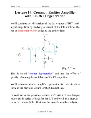
- 1. Whites, EE 320 Lecture 19 Page 1 of 10 © 2009 Keith W. Whites Lecture 19: Common Emitter Amplifier with Emitter Degeneration. We’ll continue our discussion of the basic types of BJT small- signal amplifiers by studying a variant of the CE amplifier that has an additional resistor added to the emitter lead: (Fig. 5.61a) This is called “emitter degeneration” and has the effect of greatly enhancing the usefulness of the CE amplifier. We’ll calculate similar amplifier quantities for this circuit as those in the previous lecture for the CE amplifier. In contrast to the previous lecture, we’ll use a T small-signal model (Re in series with re) for the BJT and we’ll also drop ro: it turns out to have little effect here but complicates the analysis.
- 2. Whites, EE 320 Lecture 19 Page 2 of 10 (Fig. 5.61b) • Input resistance, Rin. From this circuit, we see directly that the input resistance at the base Rib is defined as i ib b v R i ≡ (1) Notice that here iv vπ≠ , unlike the CE amplifier w/o emitter degeneration. Referring to the small-signal circuit we see that ( )i e e ev i r R= + (2) and 1 e b i i β = + (3) Substituting these into (1) gives ( )( )1ib e eR r Rβ= + + (5.127),(4) We see from this expression that the base input resistance is β+1 times the total resistance in the emitter circuit. This is called the resistance reflection rule. [In the previous lecture, we see in Fig. 5.60(b) that
- 3. Whites, EE 320 Lecture 19 Page 3 of 10 ibR rπ= but ( )1 er rπ β= + , which obeys this resistance reflection rule since there is no Re in that circuit.] This base input resistance can be much larger than without the emitter resistance. That’s often a good thing. The designer can change Re to achieve a desired input resistance [> (β+1)re]. The total input resistance to this CE amplifier with emitter degeneration is then ( )( )in || || 1B ib B e eR R R R r Rβ⎡ ⎤= = + +⎣ ⎦ (5.125),(5) • Small-signal voltage gain, Gv. We’ll first calculate the partial voltage gain o v i v A v ≡ (6) At the output, ( )||o e C Lv i R Rα= − (7) Substituting for ie from (2) gives ( )||C L v e e R R A r R α− = + (5.129),(8) The overall (from the input to the output) small-signal voltage gain Gv is defined as sig o v v G v ≡ (9)
- 4. Whites, EE 320 Lecture 19 Page 4 of 10 We can equivalently write this voltage gain as ( )6sig sig i o i v v i v v v G A v v v = ⋅ = (10) with Av given in (8). By simple voltage division at the input to the small-signal equivalent circuit in sig in sig i R v v R R = + (11) Substituting this result and (8) into (10) yields the final expression for the overall small-signal voltage gain ( ) in sig in sig ||C Lo v e e R Rv R G v r R R R α− = = + + (12) Using Rin in (5) and assuming B ibR R then (12) simplifies to ( ) ( )( )sig || 1 C L v e e R R G R r R β β − ≈ + + + (5.135),(13) Notice that this gain is actually smaller than the CE amplifier without emitter degeneration [because of the (β+1)Re term in the denominator]. However, because of this term it can be shown that the gain is less sensitive to variations in β. • Overall small-signal current gain, Gi. By definition o i i i G i ≡ (14)
- 5. Whites, EE 320 Lecture 19 Page 5 of 10 Using current division at the output of the small-signal equivalent circuit above C C o c e C L C L R R i i i R R R R α− − = = + + (15) while at the input B b i B ib R i i R R = + (16) Substituting ( )1e bi iβ= + and (16) into (15) gives ( )1C B o i C L B ib R R i i R R R R α β − = + + + or ( )( ) B C i C L B ib R R G R R R R β− = + + (17) • Short circuit current gain, Ais. In the case of a short circuit load (RL = 0), Gi reduces to the short circuit current gain: B is B ib R A R R β− = + (18) In the usual circumstance when B ibR R , then isA β≈ − (19) which is the same value as for a CE amplifier since there is no Re in this expression. • Output resistance, Rout. Referring to the small-signal equivalent circuit above and shorting out the input vsig = 0 out CR R= (20)
- 6. Whites, EE 320 Lecture 19 Page 6 of 10 which is the same as the CE amplifier (when ignoring ro). Example N19.1 (based on text exercise 5.44). Given a CE amplifier with emitter degeneration having sig 5LR R= = kΩ. The circuit is biased as in Exercise 5.41: (Fig. E5.41a) The small-signal equivalent circuit for this CE amplifier with emitter degeneration is the same as that shown in the previous lecture:
- 7. Whites, EE 320 Lecture 19 Page 7 of 10 (Fig. 5.61b) With 1EI = mA, then 25 mV 1 mA 25e T Er V I= = = Ω. • Find the value of Re that gives s gn ii 04 2R R= = kΩ. From (5) in ||B ibR R R= , which implies that 25ibR = kΩ. Using (4) ( )( )1ib e eR r Rβ= + + ⇒ 1 ib e e R r R β + = + or 25,000 225 1 1 22.5 01 ib ee R R r β = − = − = + Ω • Determine the output resistance. From (20), out 8CR R= = kΩ • Compute the overall small-signal voltage gain. Using (12) ( ) in sig in sig ||C Lo v e e R Rv R G v r R R R α− = = + + ( )0.99 3,080 20,000 25 222.5 20,000 5,000 9.86vG − = = − + + V/V
- 8. Whites, EE 320 Lecture 19 Page 8 of 10 • Determine the open circuit small-signal voltage gain, Gvo. This is the overall gain but with an open circuit load. Hence, from this description we can define L vo v R G G =∞ = Using (12) once again but with LR = ∞ gives for the CE amplifier with emitter degeneration ( )( ) in in sig C vo e e R R G r R R R α− = + + (21) For this particular amplifier ( )( ) 0.99 8,000 20,000 25 222.5 20,00 25.6 0 5,000 voG − ⋅ ⋅ = = + − + V/V Note that this is not the same open circuit gain Avo used in the text. Avo is the partial open circuit voltage gain L vo v R A A =∞ = which using (8) is C vo e e R A r R α− = + (5.131),(22) For this amplifier 0.99 8,000 25 22 2 .5 3 2 voA − ⋅ = = + − V/V Can you physically explain why Gvo and Avo are different values? • Compute the overall current gain and the short circuit current gain. Using (17)
- 9. Whites, EE 320 Lecture 19 Page 9 of 10 ( )( ) ( )( ) 100 100,000 8,000 8,000 5,000 100,000 25 49.2 A/A ,000 B C C L B i i b R R R R R G R β− = + + − ⋅ ⋅ = = + − + For the short circuit current gain, we use (18) 100 100,000 100,00 80 A/A 0 25,000 B B ib is R R R A β− − − ⋅ = = = + + • If vπ is limited to 5 mV, what is the maximum value for vsig with and without Re included? Find the corresponding vo. To address this question, we need an expression relating vsig and vπ. From (11) we know that in sig in sig i R v v R R = + (11) while at the input to the small-signal equivalent circuit above e i e e r v v r R π = + (23) Substituting (11) into (23) gives in sig sig in e e e R R r R v v R r π + + = (24) With 5vπ = mV, then sig 2520,000 5,000 5 mV 20,000 25 eR v ++ = or ( )sig 0.25 25 mVev R= + (25)
- 10. Whites, EE 320 Lecture 19 Page 10 of 10 If Re = 0, then from (25) sig 6.25v = mV is the maximum input signal voltage and because 9.86vG = − V/V, the corresponding output voltage is sig 61.6vov G v= = − mV. If Re = 222.5 Ω, then from (25) sig 61.9v = mV is the maximum input signal voltage and the corresponding output voltage is 610.1ov = − mV. This is a demonstration of yet another benefit of emitter degeneration: the amplifier can handle larger input signals (and hence potentially larger output voltages) without incurring nonlinear distortion.