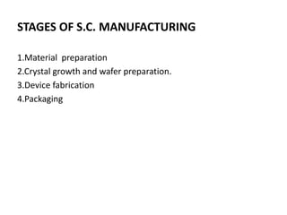
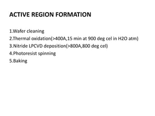
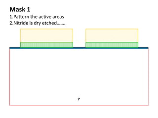
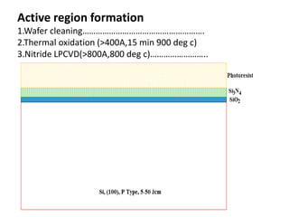
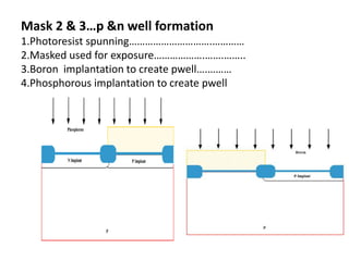
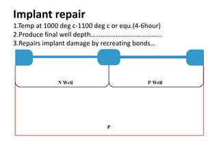
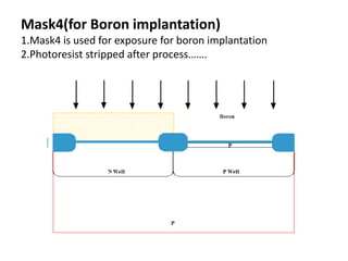
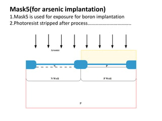
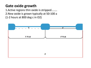
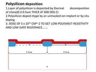
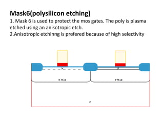
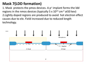
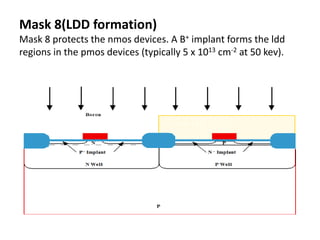
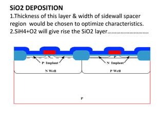
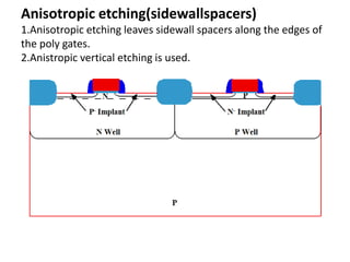
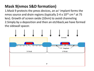
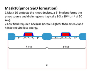
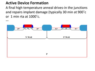
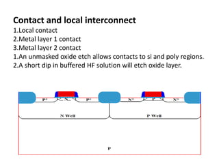
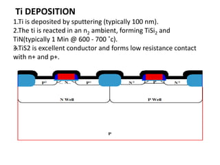
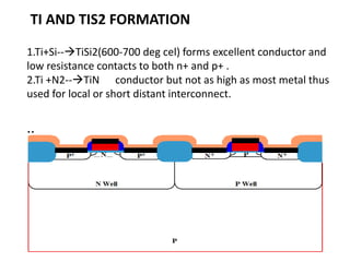
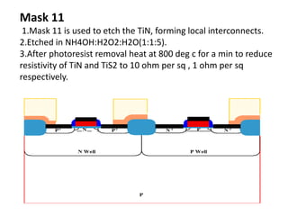
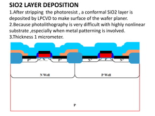
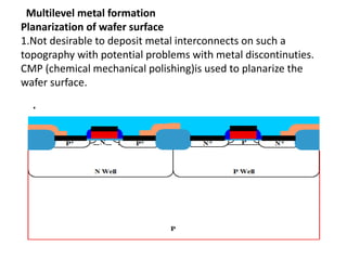
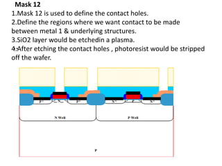
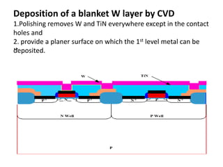
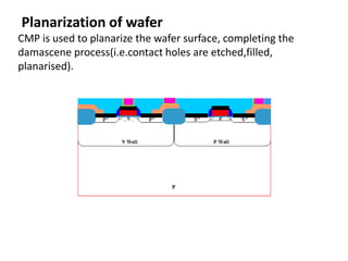
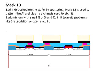
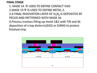
This document describes the key process steps in CMOS fabrication. It involves 16 masks and steps including active region formation through thermal oxidation and implantation, gate oxide growth, polysilicon deposition and etching, LDD and source-drain implantation, contact formation through Ti deposition and silicidation, multilevel metal interconnect formation through Al and TiN deposition, patterning and planarization. The goal is to produce n-type and p-type transistors on a silicon substrate and connect them to form integrated circuits through multiple metal interconnect layers.