Digital Electronics and Integrated Circuits - Unit 4
•
0 likes•5 views

Sri Ramakrishna College of Arts and Science, Coimbatore, Department of Physics, Digital Electronics and Integretad Circuits-Unit 4.

Recommended
More Related Content
Similar to Digital Electronics and Integrated Circuits - Unit 4
Similar to Digital Electronics and Integrated Circuits - Unit 4 (20)
More from Dhivya Ramachandran
More from Dhivya Ramachandran (15)
Recently uploaded
Recently uploaded (20)
Digital Electronics and Integrated Circuits - Unit 4
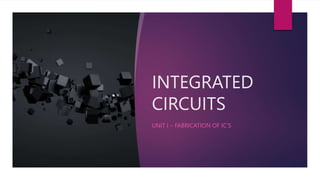
- 1. INTEGRATED CIRCUITS UNIT I – FABRICATION OF IC’S
- 2. COMPONENTS ACTIVE COMPONENT: Active components such as transistors and silic on-controlled rectifiers (SCRs) use electricity to control electricity PASSIVE COMPONENT: Passive components like resistors, transformers, and diodes don't need an external power source to function In an electronic circuit these components have to be connected by soldered wires.
- 3. EVOLUTION OF ICs Invention of transistor – 1948 – W.H. Brattain & I. Bardeen – circuits are reduced in size Development of PCB further reduced the size of the circuits New field of microelectronics – due to military needs – 1960 (1/10 of existing size) This led to the development of microelectronic circuits called Integrated Circuits (ICs) – very small in size – construction done under high powered microscopes What are ICs?
- 4. INTEGRATED CIRCUITS IC – Packaged electronic Circuit Both active and passive components are fabricated into a single chip of silicon
- 5. Advantages and Limitations ADVANTAGES Extremely small physical size, Light weight, Reduced cost, Extremely high reliability, Increased response time and speed, Low power consumption, Easy replacement & higher yield. LIMITATIONS Coils or inductors cannot be fabricated ICs Function at fairly low voltage They can handle only limited amount of power Delicate & cannot withstand rough handling
- 6. Scale of Integration SlNo Scale Ckts/Pkg Approx No of Components 1 Small Scale Integration(SSI) <12 <50 2 Medium Scale Integration(MSI) 13-99 50-5000 3 Large Scale Integration (LSI) 100-99,999 5000-1,00,000 4 Very Large Scale Integration (VLSI) 10,000-99,999 1,00,000-10,00,000 5 Ultra Large Scale Integration (ULSI) 1,00,000-9,99,999 10,00,000-1,00,00,000 6 Giga Scale Integration (GSI) >1,00,000 >1,00,00,000 7 System On Chip (SOC and 3D-IC) All Components needed for a computer
- 8. Linear Integrated Circuits Also referred to as Analog ICs I/p and O/p can take continuous range of values O/p 𝛼 I/P Less used than Digital ICs They are replacing discreate circuit conterparts in many circuits They are highly reliable due to elimination of external connections Used widely in military, industrial applications and in consumer products
- 9. Linear Integrated Circuits They are frequently used in Operational amplifiers Small-Signal Amplifiers Power Amplifiers RF and IF Amplifiers Microwave Amplifiers Multipliers Voltage Amplifiers Voltage Regulators
- 10. Manufacturer’s Designation of LICs Each Manufacturer – Specific code and type number EG Internally Compensated Op-Amp – 741 Sl No Manufacturer’s Name Designation 1 Fairchild mA 741 2 National Semiconductor LM 741 3 Motorola MC 1741 4 RCA CA 3741 5 Texas Instruments SN 52741
- 11. Manufacturer’s Designation of LICs MANY LICS ARE DESIGNED UNDER DIFFERENT CLASSES Sl No Class Definition 1 741 Military Grade Op-Amps 2 741 C Commercial Grade Op-Amps 3 741 A Improved Version of 741 4 741 E Improved Version of 741 C 5 741 S Military Grade Op-Amp with higher Slew Rate 6 741 SE Commercial Grade Op-Amps with Higher Slew Rate
- 12. Digital Integrated Circuits Mostly Utilized in Computer Industry Monolithic integration Employs very few capacitors Values of resistances, voltages and currents are low I/P and O/P are limited to two possible levels – High or Low Digital signals are usually binary Some digital circuits are referred to as switching circuits
- 13. Digital Integrated Circuits Logic Gates Flip-flops Counters Clock-chips Calculator chips Memory chips Microprocessor etc
- 14. Crystal Growing and Wafer Preparation Poly crystalline silicon – Random orientation and defects For IC Fabrication – Si – has to be Pure and crystalline There is a need to produce single crystal of silicon – crystal growth Crystal growth Czochralski Flat zone
- 16. Czochralski Process Equipment – Puller Puller Furnace Quartz Crucible Rotation mechanism RF Heating Element Pulling Mechanism Seed holder Pull & rotate mechanism Ambient Control Argon gas source Flow control Exhaust system
- 17. Procedure Polycrystalline silicon is placed in the crucible Furnace temperature – 1690 K (melting point of Si – 1685 K) Precisely controlled amount of dopant (B or P) to make the melt P or N type Seed crystal is suspended in the seed holder Seed is inserted into the melt and a small portion of is allowed to melt Seed is rotated in the CCW direction and pulled very slowly At the same time, the crucible is rotated in the CW direction The melt attaches to the seed and grows in the similar manner as the seed as it is pulled out it solidifies Cylindrical single crystal bars(Ingots) of silicon are produced
- 18. Wafer Preparation The cooled Ingots can be made into thin discs called WAFERS The ingots have diameters as large as 200mm and length upto 1000mm Ground Top bottom cutoff Flat regions slicing
- 20. Wafer Fabrication Oxidation Etching Diffusion Ion Implantation Photolithography Epitaxy Metallization and interconnections
- 21. Oxidation Oxide layer grown in Si Surface Advantages of SiO2 To serve as a mask against implant or diffusion of dopant into silicon To provide surface passivation To isolate one device from another To act as a component in MOS structure Thermal Oxidation, CVD, Plasma oxidation can be utilized to form oxidation
- 22. Oxidation Thermal Oxidation System Working Oxygen atm 1000 deg C Dry – Watervapour and Oxygen Rate of Oxidation – Slow Electrical Properties – Excellent
- 23. Etching Selective removal of regions of semiconductor, Metal or Silicon Di Oxide layer Wet – Immersed in chemical solution - Isotropic Dry – Immersed in Gaseous plasma – RIF - anisotropic Etching Wet Dry
- 24. Diffusion Process Introduction of impurities into selected region of the wafer to form junction Steps: Pre-Deposition Drive-in diffusion Pre-Deposition (Ion – Implantation) Dopant in vapour – high concentration @ 1000 deg C Produces shallow heavily doped layer near silicon surface Drive in – drive the impurity deeper in to the surface without adding more Dopant Profiles
- 25. Diffusion P – Dopant atoms Deposited Silicon Dioxide P-type silicon Dopant atoms diffused in Si but not in SiO2
- 26. Ion Implantation Ion Implantation System Process Dopant introduction by bombarding with high energy ion of the dopant. Arc discharge Accelerated in electric field Focussed to strike on Si Wafer Depth of penetration: 0.1 to 1mm Higher the energy and mass-deeper the penetration
- 27. Advantage and Disadvantages of Ion Implantation over Diffusion Advantages Doping Levels can be precisely controlled Depth of dopant can be regulated Guaranteed purity of dopant Uniformity of doping Doping area con be clearly defined No temperature stress – room temperature No need for thick masking oxide layers Disadvantages Damage is caused to the crystal structure High initial investment and operational cost ( US 1 Million) High Toxic gas is used for some dopants (Phosphorous & arsenic)
- 28. Photolithography Steps Involved Process Geometrical pattern on a glass pate (reticle) is transferred to the surface of wafer Wafer to be coated with light sensitive material called photoresist over the oxide layer
- 29. Photolithography • Baking • 100°C Wafer • On wafer • aligned Glass plate • UV exposed • Opaque unaffected Glass plate Exposed- chemically removes- organic solvents Photo Resist Etched using HF SiO2 Opaque- removed using proper solvent Photore sist
- 30. Epitaxy Controlled growth of a crystalline doped layer of silicon on a single crystal substrate Used to dope N ot N+ Methods VPE LPE MBE Temp – 1200 deg C