The Czochralski method is used to grow large single crystal boules of semiconductors like silicon that are then cut into wafers for manufacturing integrated circuits. In the process, a seed crystal is dipped into a melt of the material held at a temperature slightly above its melting point. The seed is slowly extracted while being rotated, allowing the melted material to solidify on the seed in a crystalline structure to form a cylindrical ingot. This ingot is then cut and polished into wafers for semiconductor device fabrication. The Czochralski method is well-suited for silicon crystal growth and is the predominant industrial process for producing silicon wafers.


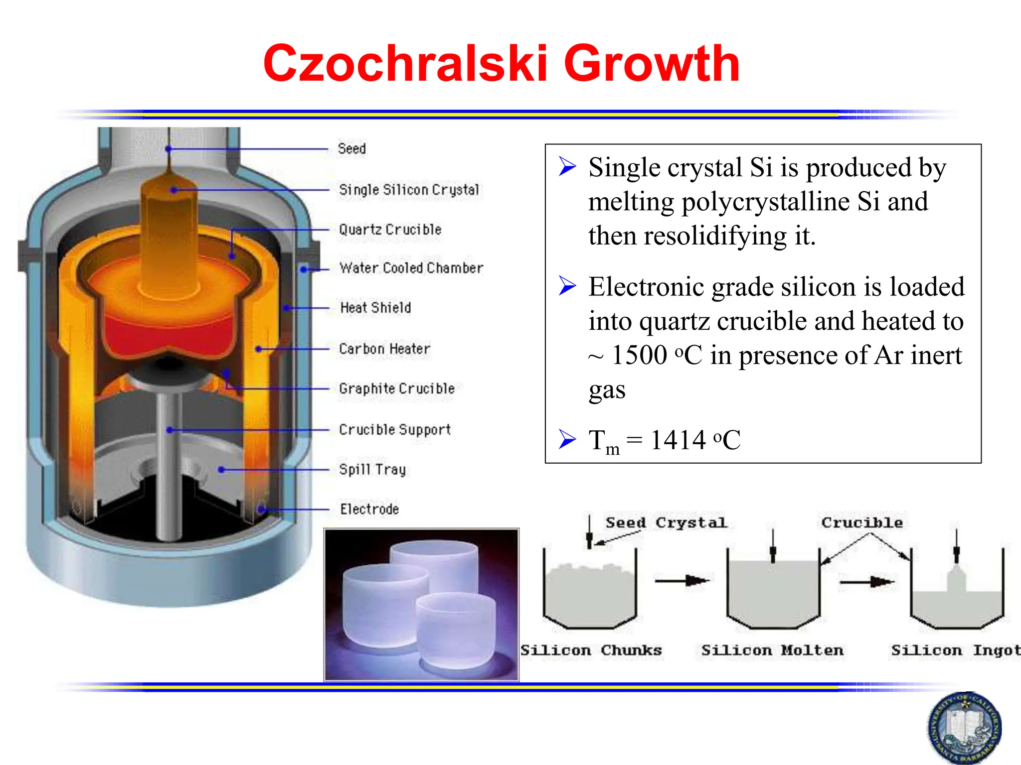


![Czochralski method
Used for crystal growth to obtain single crystals of
semiconductors(e.g. silicon, germanium, GaAS), metals (e.g.
palladium, platinum, silver, gold), salts and synthetic gemstones.
It is also known as Pulling Technique
In the Czochralski process a seed crystal is required to create a
larger crystal, or ingot. This seed crystal is dipped into the pure
molten silicon and slowly extracted. The molten silicon grows on
the seed crystal in a crystalline fashion. As the seed is extracted
the silicon solidifies and eventually a large, cylindrical boule is
produced.[3]
In this method the charge is melted and maintained at a
temperature slightly above the melting point. The pulling rod is
lowered to just touch the melt. Since the rod is at lower
temperature of melt occurs at the point tip of the pulling rod.
The crystal is pulled slowly.](https://image.slidesharecdn.com/czmdpptmjunit-1-231107110240-0691d01e/75/CZ-md_ppt_mj_unit-1-pptx-12-2048.jpg)

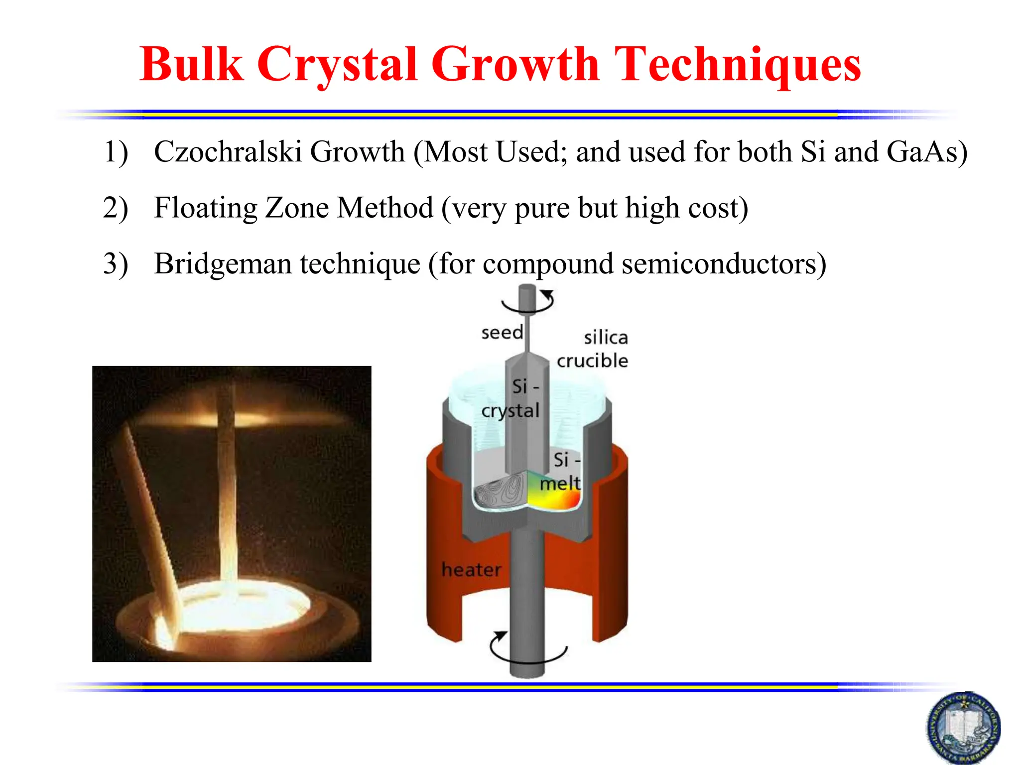
![Czochralski method
1. A boule is a single-crystal ingot produced by synthetic means.[1]
2. A boule of silicon is the starting material for most of
the integrated circuits used today.
3. In the semiconductor industry synthetic boules can be made by a
number of methods, such as the Bridgman technique[2] and
the Czochralski process, which result in a cylindrical rod of material.
In the Czochralski process a seed crystal is required to create a
larger crystal, or ingot. This seed crystal is dipped into the pure
molten silicon and slowly extracted. The molten silicon grows on
the seed crystal in a crystalline fashion. As the seed is extracted the
silicon solidifies and eventually a large, cylindrical boule is
produced.[3]
A semiconductor crystal boule is normally cut into
circular wafers using an inside hole diamond saw or diamond wire
saw, and each wafer is lapped and polished to provide substrates
suitable for the fabrication of semiconductor devices on its
surface.[4]](https://image.slidesharecdn.com/czmdpptmjunit-1-231107110240-0691d01e/75/CZ-md_ppt_mj_unit-1-pptx-14-2048.jpg)


