Download as PDF, PPTX

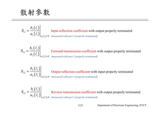
![•
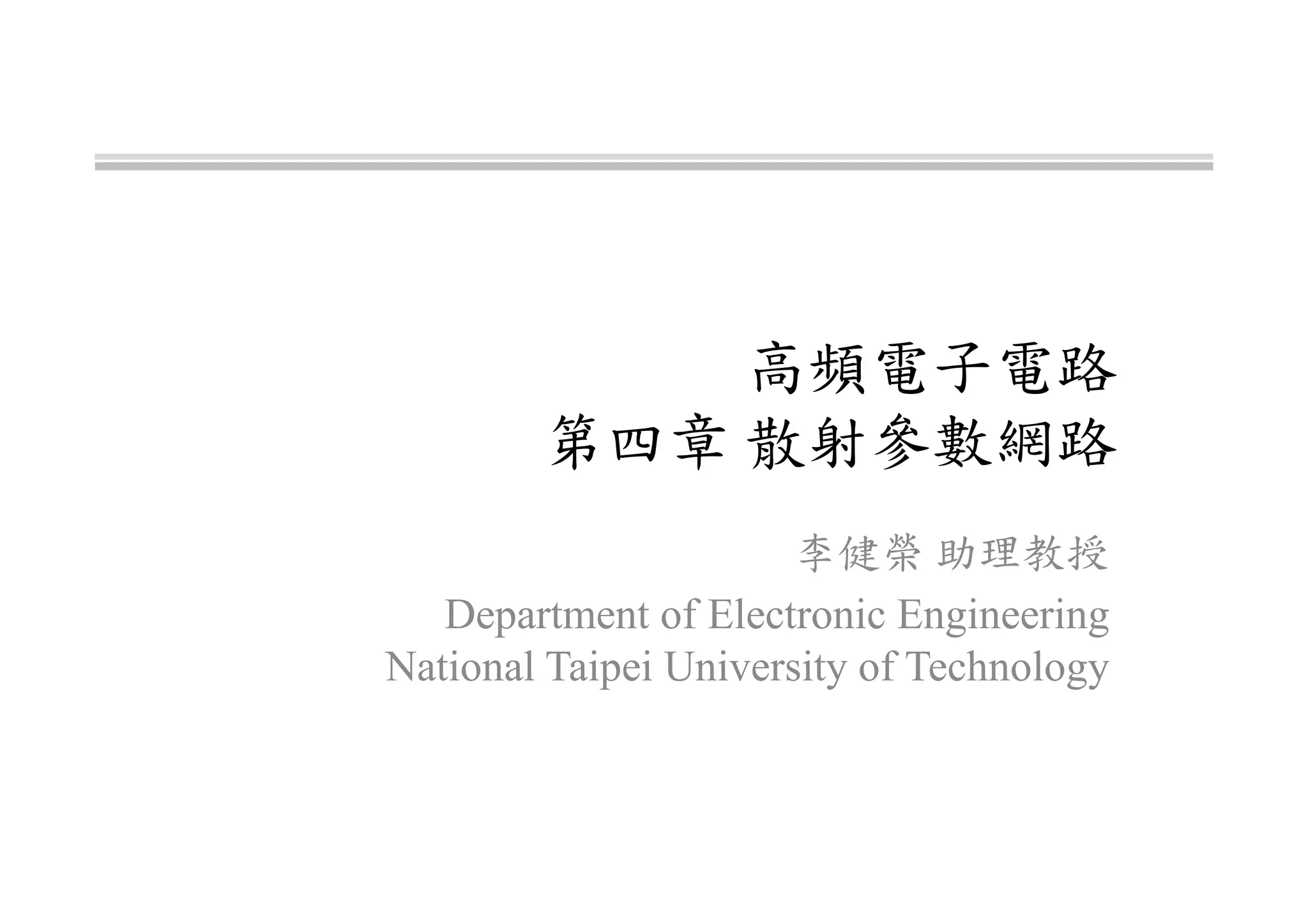
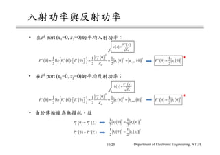
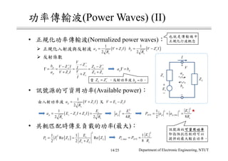
Zoi (i=1 to n) n port
[ ] [ ][ ]b S a=
n-port
Network
1oZ
Port 1Port 1'
1TZ
( )1 1a l
( )1 1b l
2oZ
Port 2Port 2'
( )2 2a l
( )2 2b l
onZ
Port nPort n'
( )n na l
( )n nb l
[ ]
11 12 1
21 22 2
1 2
n
n
n n nn
S S S
S S S
S
S S S
⋅ ⋅
⋅ ⋅
= ⋅ ⋅ ⋅ ⋅ ⋅
⋅ ⋅ ⋅ ⋅ ⋅
⋅ ⋅
8/25 Department of Electronic Engineering, NTUT](https://image.slidesharecdn.com/ch4-150613065103-lva1-app6891/85/slide-8-320.jpg)
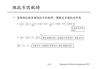
![− (Traveling Waves)
0
0
s
s
s
Z Z
Z Z
−
Γ =
+
0
0
L
L
L
Z Z
Z Z
−
Γ =
+
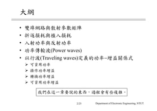
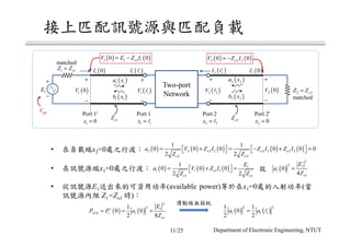
1 11 1 12 2b S a S a= +
2 21 1 22 2b S a S a= +
Transistor
[S]
2a
2b
1a
1b
Port 1 Port 2
+
−
sE
sZ
outΓ
LZ
inΓ
sΓ LΓ
•
[S] Z0
sΓ LΓ
?
+
−
sE
sZ
sΓ
LZ
LΓ
Transistor
[S]
1b
1a 2a
2b
16/25 Department of Electronic Engineering, NTUT](https://image.slidesharecdn.com/ch4-150613065103-lva1-app6891/85/slide-16-320.jpg)
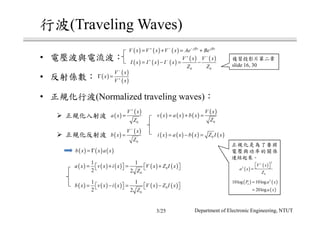
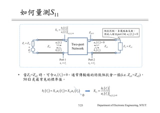
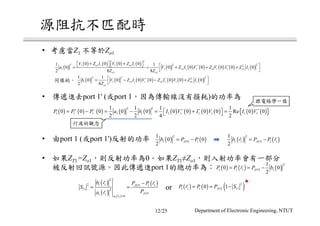
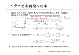
![1
1
in
b
a
Γ =
2 2La b= Γ
2 21 1 22 2Lb S a S b= + Γ 21 1
2
221 L
S a
b
S
=
− Γ
• inΓ
[ ]SLΓ
1 12 21
11
1 221
L
in
L
b S S
S
a S
Γ
Γ = = +
− Γ
12 21
1 11 1 12 2 11 1 1
221
L
L
L
S S
b S a S b S a a
S
Γ
= + Γ = +
− Γ
a1 b1
1 11 1 12 2b S a S a= +
a1 b1 = a2
a2 = b2
Transistor
[S]
2a
2b
1a
1b
+
−
sE
sZ
outΓ
LZ
inΓ
sΓ LΓ
1 11 1 12 2b S a S a= +
2 21 1 22 2b S a S a= +
inΓ
17/25 Department of Electronic Engineering, NTUT](https://image.slidesharecdn.com/ch4-150613065103-lva1-app6891/85/slide-17-320.jpg)
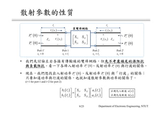
![2
2 0s
out
E
b
a =
Γ =
1 1sa b= Γ
1 11 1 12 2sb S b S a= Γ + 12 2
1
111 s
S a
b
S
=
− Γ
12 21
2 21 1 22 2 2 22 2
111
s
s
s
S S
b S b S a a S a
S
Γ
= Γ + = +
− Γ
12 212
22
2 110
1
s
s
out
sE
S Sb
S
a S=
Γ
Γ = = +
− Γ
• outΓ
[ ]SsΓ
Transistor
[S]
2a
2b
1a
1b
+
−
sE
sZ
outΓ
LZ
inΓ
sΓ LΓ
1 11 1 12 2b S a S a= +
2 21 1 22 2b S a S a= +
outΓ
outΓ inΓ
2 21 1 22 2b S a S a= +and
18/25 Department of Electronic Engineering, NTUT](https://image.slidesharecdn.com/ch4-150613065103-lva1-app6891/85/slide-18-320.jpg)
![Transistor
[S]+
−
sE
sZ
LZ
PAVNPAVS PLPin
Ms
interface interface
ML
• (power gain) L
p
in
P
G
P
=
• (transducer power gain) L
T p s
AVS
P
G G M
P
= =
• (available power gain) AVN T
A
AVS L
P G
G
P M
= =
p TG G>
A TG G>
• p T AG G G= =
21/25 Department of Electronic Engineering, NTUT](https://image.slidesharecdn.com/ch4-150613065103-lva1-app6891/85/slide-21-320.jpg)
![Gp (Operating Power Gain)
( )
( )
2 2
2
2 2
1
1
1
2
1
1
2
L
L
p
in
in
b
P
G
P a
− Γ
= =
− Γ
21 1
2
221 L
S a
b
S
=
− Γ
2
2
212 2
22
11
1 1
L
p
in L
G S
S
− Γ
=
− Γ − Γ
• The Operating Power Gain Gp
where
Transistor
[S]+
−
sE
sZ
LZ
PAVNPAVS PLPin
Ms
interface interface
ML
slide 17
22/25 Department of Electronic Engineering, NTUT](https://image.slidesharecdn.com/ch4-150613065103-lva1-app6891/85/slide-22-320.jpg)
![GT (Transducer Power Gain)
• The Transducer Power Gain GT
in inL L
T p p s
AVS in AVS AVS
P PP P
G G G M
P P P P
= = = =
2 2 2 2
2 2
21 212 2 2 2
22 11
1 1 1 1
1 1 1 1
s L s L
T
s in L s out L
G S S
S S
− Γ − Γ − Γ − Γ
= =
− Γ Γ − Γ − Γ − Γ Γ
( )( )2 2
2
1 1
1
s in
s
s in
M
− Γ − Γ
=
− Γ Γ
where
Transistor
[S]+
−
sE
sZ
LZ
PAVNPAVS PLPin
Ms
interface interface
ML
slide 19
23/25 Department of Electronic Engineering, NTUT](https://image.slidesharecdn.com/ch4-150613065103-lva1-app6891/85/slide-23-320.jpg)
![GA (Available Power Gain)
• The Available Power Gain GA
AVN AVN AVNL T
A T
AVS AVS L L L
P P PP G
G G
P P P P M
= = = =
2
2
212 2
11
1 1
1 1
s
A
s out
G S
S
− Γ
=
− Γ − Γ
Transistor
[S]+
−
sE
sZ
LZ
PAVNPAVS PLPin
Ms
interface interface
ML
( )( )2 2
2
1 1
1
L out
L
out L
M
− Γ − Γ
=
− Γ Γ
where
slide 20
24/25 Department of Electronic Engineering, NTUT](https://image.slidesharecdn.com/ch4-150613065103-lva1-app6891/85/slide-24-320.jpg)
![•
(1) ( )
(2) (power waves, [Sp])
(3) (traveling waves, [S])
{ }Re 2L L LP V I∗
=
• ( )
2
2 2
,
1
2 8
s
AVS p p rms
s
E
P a a
R
= = =
2 2 21 1 1
2 2 2
L p p AVS pP a b P b= − = −
•
L p inP G P= L T AVSP G P=
• (defined with traveling waves, circuitries are
separately measured in a Zo system) :
25/25 Department of Electronic Engineering, NTUT](https://image.slidesharecdn.com/ch4-150613065103-lva1-app6891/85/slide-25-320.jpg)

This document discusses traveling waves and scattering parameters for analyzing multi-port networks. It begins by defining traveling waves as voltage and current waves that propagate through transmission lines. It then introduces scattering parameters (S-parameters) which describe the input-output relationship of linear electrical networks with multiple ports. S-parameters are presented as elements of a scattering matrix that relates incoming and outgoing wave amplitudes at each port. Methods for calculating reflection and transmission coefficients from S-parameters are provided for characterizing two-port networks. The analysis is then generalized to n-port networks using scattering matrices. Key parameters like return loss, insertion loss, and available power are defined in terms of S-parameters.
![射頻電子 - [第一章] 知識回顧與通訊系統簡介](https://cdn.slidesharecdn.com/ss_thumbnails/ch1-150613065058-lva1-app6891-thumbnail.jpg?width=640&height=640&fit=bounds)
![射頻電子 - [實驗第四章] 微波濾波器與射頻多工器設計](https://cdn.slidesharecdn.com/ss_thumbnails/e4-150613065110-lva1-app6892-thumbnail.jpg?width=640&height=640&fit=bounds)
![射頻電子 - [實驗第一章] 基頻放大器設計](https://cdn.slidesharecdn.com/ss_thumbnails/e1-150613065108-lva1-app6892-thumbnail.jpg?width=640&height=640&fit=bounds)
![射頻電子 - [第六章] 低雜訊放大器設計](https://cdn.slidesharecdn.com/ss_thumbnails/ch6-150613065106-lva1-app6892-thumbnail.jpg?width=640&height=640&fit=bounds)
![射頻電子 - [第二章] 傳輸線理論](https://cdn.slidesharecdn.com/ss_thumbnails/ch2-150613065059-lva1-app6891-thumbnail.jpg?width=640&height=640&fit=bounds)
![射頻電子 - [第五章] 射頻放大器設計](https://cdn.slidesharecdn.com/ss_thumbnails/ch5-150613065105-lva1-app6892-thumbnail.jpg?width=640&height=640&fit=bounds)
![射頻電子 - [實驗第三章] 濾波器設計](https://cdn.slidesharecdn.com/ss_thumbnails/e3-150613065109-lva1-app6891-thumbnail.jpg?width=640&height=640&fit=bounds)
![射頻電子 - [第三章] 史密斯圖與阻抗匹配](https://cdn.slidesharecdn.com/ss_thumbnails/ch3-150613065103-lva1-app6892-thumbnail.jpg?width=640&height=640&fit=bounds)
![射頻電子實驗手冊 [實驗1 ~ 5] ADS入門, 傳輸線模擬, 直流模擬, 暫態模擬, 交流模擬](https://cdn.slidesharecdn.com/ss_thumbnails/simlab15-150613072411-lva1-app6892-thumbnail.jpg?width=640&height=640&fit=bounds)
![射頻電子實驗手冊 [實驗6] 阻抗匹配模擬](https://cdn.slidesharecdn.com/ss_thumbnails/simlab6-150613072411-lva1-app6892-thumbnail.jpg?width=640&height=640&fit=bounds)
![Agilent ADS 模擬手冊 [實習3] 壓控振盪器模擬](https://cdn.slidesharecdn.com/ss_thumbnails/3adsosc-150613072819-lva1-app6892-thumbnail.jpg?width=640&height=640&fit=bounds)
![射頻電子實驗手冊 - [實驗7] 射頻放大器模擬](https://cdn.slidesharecdn.com/ss_thumbnails/simlab7-150613072420-lva1-app6892-thumbnail.jpg?width=640&height=640&fit=bounds)

![Agilent ADS 模擬手冊 [實習1] 基本操作與射頻放大器設計](https://cdn.slidesharecdn.com/ss_thumbnails/1adsbasics-150613072812-lva1-app6891-thumbnail.jpg?width=640&height=640&fit=bounds)
![射頻電子實驗手冊 - [實驗8] 低雜訊放大器模擬](https://cdn.slidesharecdn.com/ss_thumbnails/simlab8-150613072425-lva1-app6891-thumbnail.jpg?width=640&height=640&fit=bounds)
![射頻電子 - [實驗第二章] I/O電路設計](https://cdn.slidesharecdn.com/ss_thumbnails/e2-150613065108-lva1-app6892-thumbnail.jpg?width=640&height=640&fit=bounds)
![電路學 - [第七章] 正弦激勵, 相量與穩態分析](https://cdn.slidesharecdn.com/ss_thumbnails/circuitch7-150613063009-lva1-app6891-thumbnail.jpg?width=640&height=640&fit=bounds)
![RF Circuit Design - [Ch3-1] Microwave Network](https://cdn.slidesharecdn.com/ss_thumbnails/ch3-1-150613064402-lva1-app6892-thumbnail.jpg?width=640&height=640&fit=bounds)
![RF Circuit Design - [Ch3-2] Power Waves and Power-Gain Expressions](https://cdn.slidesharecdn.com/ss_thumbnails/ch3-2-150613064404-lva1-app6891-thumbnail.jpg?width=640&height=640&fit=bounds)
![Multiband Transceivers - [Chapter 2] Noises and Linearities](https://cdn.slidesharecdn.com/ss_thumbnails/ch2-150613070933-lva1-app6892-thumbnail.jpg?width=640&height=640&fit=bounds)
![Agilent ADS 模擬手冊 [實習2] 放大器設計](https://cdn.slidesharecdn.com/ss_thumbnails/2adsamp-150613072818-lva1-app6892-thumbnail.jpg?width=640&height=640&fit=bounds)
![電路學 - [第八章] 磁耦合電路](https://cdn.slidesharecdn.com/ss_thumbnails/circuitch8-150613063010-lva1-app6892-thumbnail.jpg?width=640&height=640&fit=bounds)
![RF Module Design - [Chapter 1] From Basics to RF Transceivers](https://cdn.slidesharecdn.com/ss_thumbnails/rfch1-150613070344-lva1-app6892-thumbnail.jpg?width=640&height=640&fit=bounds)
![Circuit Network Analysis - [Chapter2] Sinusoidal Steady-state Analysis](https://cdn.slidesharecdn.com/ss_thumbnails/ch2-150613063856-lva1-app6892-thumbnail.jpg?width=640&height=640&fit=bounds)
![電路學 - [第六章] 二階RLC電路](https://cdn.slidesharecdn.com/ss_thumbnails/circuitch6-150613063009-lva1-app6892-thumbnail.jpg?width=640&height=640&fit=bounds)
![RF Circuit Design - [Ch2-2] Smith Chart](https://cdn.slidesharecdn.com/ss_thumbnails/ch2-2-150613064401-lva1-app6891-thumbnail.jpg?width=640&height=640&fit=bounds)
![RF Circuit Design - [Ch1-1] Sinusoidal Steady-state Analysis](https://cdn.slidesharecdn.com/ss_thumbnails/ch1-1-150613064348-lva1-app6891-thumbnail.jpg?width=640&height=640&fit=bounds)

![RF Circuit Design - [Ch4-2] LNA, PA, and Broadband Amplifier](https://cdn.slidesharecdn.com/ss_thumbnails/ch4-2-150613064410-lva1-app6891-thumbnail.jpg?width=640&height=640&fit=bounds)
![RF Circuit Design - [Ch2-1] Resonator and Impedance Matching](https://cdn.slidesharecdn.com/ss_thumbnails/ch2-1-150613064353-lva1-app6892-thumbnail.jpg?width=640&height=640&fit=bounds)
![RF Circuit Design - [Ch1-2] Transmission Line Theory](https://cdn.slidesharecdn.com/ss_thumbnails/ch1-2-150613064349-lva1-app6892-thumbnail.jpg?width=640&height=640&fit=bounds)
![Circuit Network Analysis - [Chapter3] Fourier Analysis](https://cdn.slidesharecdn.com/ss_thumbnails/ch3-150613063858-lva1-app6891-thumbnail.jpg?width=640&height=640&fit=bounds)
![Circuit Network Analysis - [Chapter1] Basic Circuit Laws](https://cdn.slidesharecdn.com/ss_thumbnails/ch1-150613063856-lva1-app6892-thumbnail.jpg?width=640&height=640&fit=bounds)
![電路學 - [第五章] 一階RC/RL電路](https://cdn.slidesharecdn.com/ss_thumbnails/circuitch5-150613063008-lva1-app6891-thumbnail.jpg?width=640&height=640&fit=bounds)
![RF Circuit Design - [Ch4-1] Microwave Transistor Amplifier](https://cdn.slidesharecdn.com/ss_thumbnails/ch4-1-150613064409-lva1-app6892-thumbnail.jpg?width=640&height=640&fit=bounds)
![Circuit Network Analysis - [Chapter4] Laplace Transform](https://cdn.slidesharecdn.com/ss_thumbnails/ch4-150613063858-lva1-app6891-thumbnail.jpg?width=640&height=640&fit=bounds)
![Circuit Network Analysis - [Chapter5] Transfer function, frequency response, ...](https://cdn.slidesharecdn.com/ss_thumbnails/ch5-150613063859-lva1-app6891-thumbnail.jpg?width=640&height=640&fit=bounds)
![電路學 - [第四章] 儲能元件](https://cdn.slidesharecdn.com/ss_thumbnails/circuitch4-150613063008-lva1-app6891-thumbnail.jpg?width=640&height=640&fit=bounds)
![電路學 - [第三章] 網路定理](https://cdn.slidesharecdn.com/ss_thumbnails/circuitch3-150613063007-lva1-app6892-thumbnail.jpg?width=640&height=640&fit=bounds)


![電路學 - [第二章] 電路分析方法](https://cdn.slidesharecdn.com/ss_thumbnails/circuitch2-150613063007-lva1-app6891-thumbnail.jpg?width=640&height=640&fit=bounds)


![Multiband Transceivers - [Chapter 1]](https://cdn.slidesharecdn.com/ss_thumbnails/ch1-150613070932-lva1-app6891-thumbnail.jpg?width=640&height=640&fit=bounds)


![[ZigBee 嵌入式系統] ZigBee Architecture 與 TI Z-Stack Firmware](https://cdn.slidesharecdn.com/ss_thumbnails/zigbeearchitecture-150613072045-lva1-app6892-thumbnail.jpg?width=640&height=640&fit=bounds)
![[ZigBee 嵌入式系統] ZigBee 應用實作 - 使用 TI Z-Stack Firmware](https://cdn.slidesharecdn.com/ss_thumbnails/zigbeeappimplementation-150613072040-lva1-app6891-thumbnail.jpg?width=640&height=640&fit=bounds)
![[嵌入式系統] MCS-51 實驗 - 使用 IAR (3)](https://cdn.slidesharecdn.com/ss_thumbnails/mcs51iarpart3-150613071723-lva1-app6892-thumbnail.jpg?width=640&height=640&fit=bounds)
![[嵌入式系統] MCS-51 實驗 - 使用 IAR (2)](https://cdn.slidesharecdn.com/ss_thumbnails/mcs51iarpart2-150613071717-lva1-app6891-thumbnail.jpg?width=640&height=640&fit=bounds)
![[嵌入式系統] MCS-51 實驗 - 使用 IAR (1)](https://cdn.slidesharecdn.com/ss_thumbnails/mcs51iarpart1-150613071712-lva1-app6892-thumbnail.jpg?width=640&height=640&fit=bounds)

![[嵌入式系統] 嵌入式系統進階](https://cdn.slidesharecdn.com/ss_thumbnails/advembedded-150613071653-lva1-app6892-thumbnail.jpg?width=640&height=640&fit=bounds)
![Multiband Transceivers - [Chapter 7] Spec. Table](https://cdn.slidesharecdn.com/ss_thumbnails/ch7table-150613070936-lva1-app6892-thumbnail.jpg?width=640&height=640&fit=bounds)
![Multiband Transceivers - [Chapter 7] Multi-mode/Multi-band GSM/GPRS/TDMA/AMP...](https://cdn.slidesharecdn.com/ss_thumbnails/ch7-150613070936-lva1-app6892-thumbnail.jpg?width=640&height=640&fit=bounds)
![Multiband Transceivers - [Chapter 6] Multi-mode and Multi-band Transceivers](https://cdn.slidesharecdn.com/ss_thumbnails/ch6-150613070935-lva1-app6891-thumbnail.jpg?width=640&height=640&fit=bounds)
![Multiband Transceivers - [Chapter 4] Design Parameters of Wireless Radios](https://cdn.slidesharecdn.com/ss_thumbnails/ch4-150613070934-lva1-app6892-thumbnail.jpg?width=640&height=640&fit=bounds)
![Multiband Transceivers - [Chapter 5] Software-Defined Radios](https://cdn.slidesharecdn.com/ss_thumbnails/ch5-150613070934-lva1-app6892-thumbnail.jpg?width=640&height=640&fit=bounds)
![Multiband Transceivers - [Chapter 3] Basic Concept of Comm. Systems](https://cdn.slidesharecdn.com/ss_thumbnails/ch3-150613070933-lva1-app6892-thumbnail.jpg?width=640&height=640&fit=bounds)
![RF Module Design - [Chapter 8] Phase-Locked Loops](https://cdn.slidesharecdn.com/ss_thumbnails/rfch8-150613070348-lva1-app6892-thumbnail.jpg?width=640&height=640&fit=bounds)


