Downloaded 357 times
![Department of Electronic Engineering, NTUT
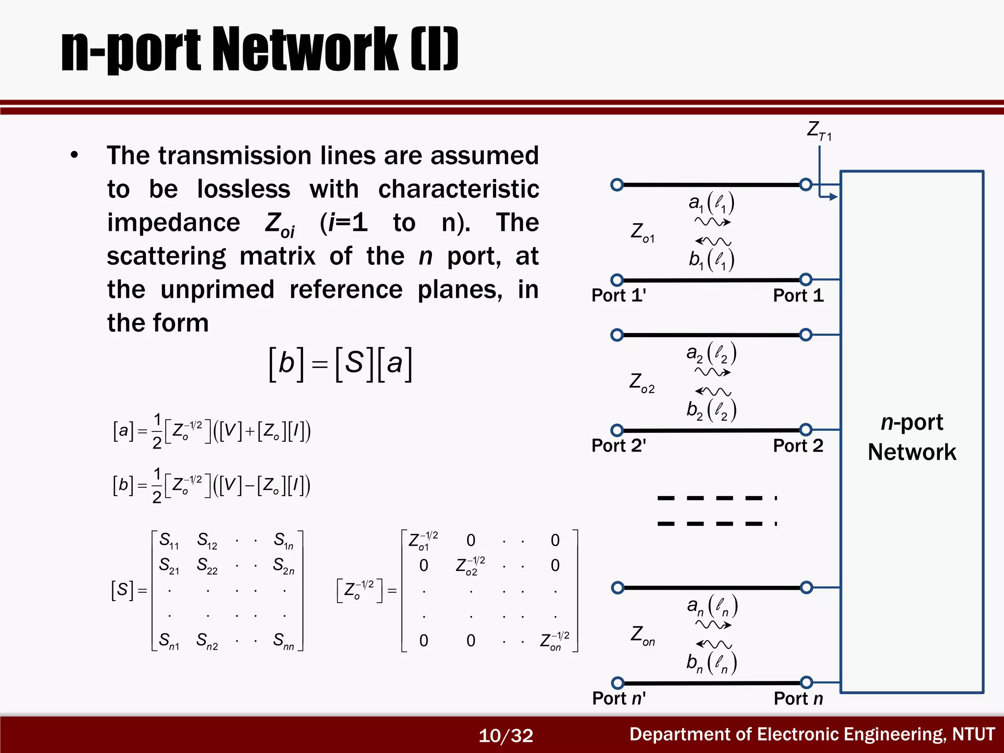
n-port Network (II)
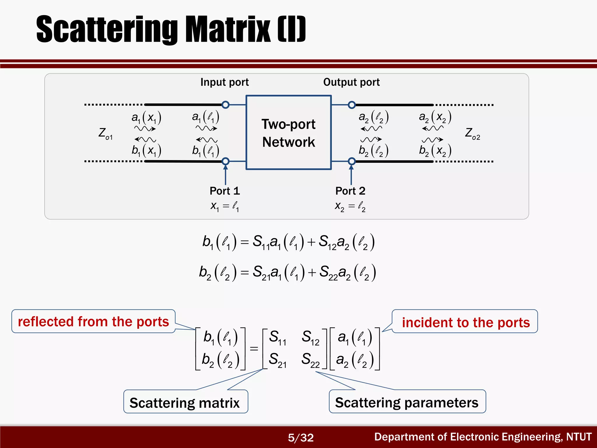
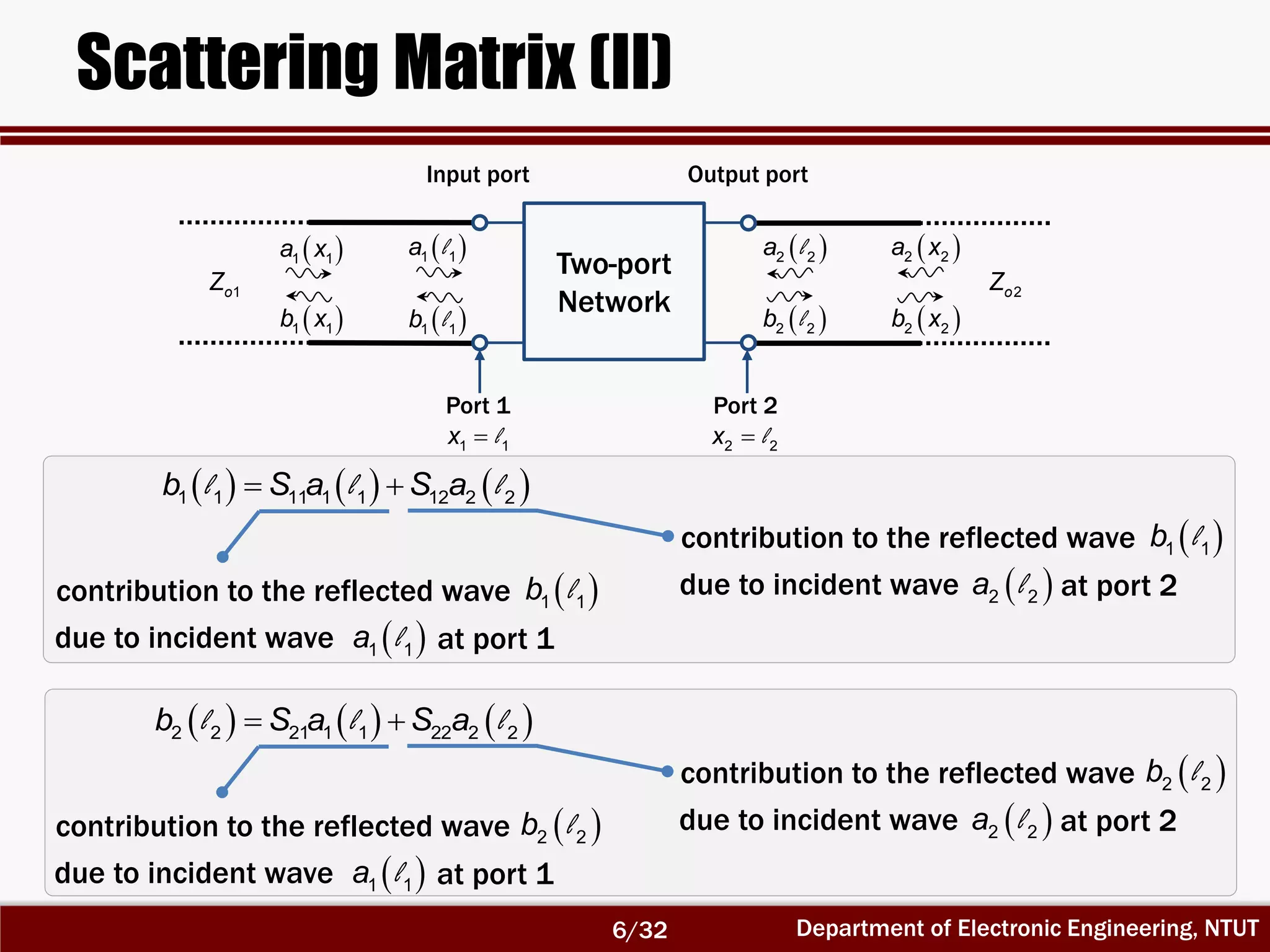
• The [a], [b], [V], and [I] are column matrices. That is
1
2
n
a
a
a
a
1
2
n
b
b
b
b
1
2
n
V
V
V
V
1
2
n
I
I
I
I
l
l
1 1 1 1
11
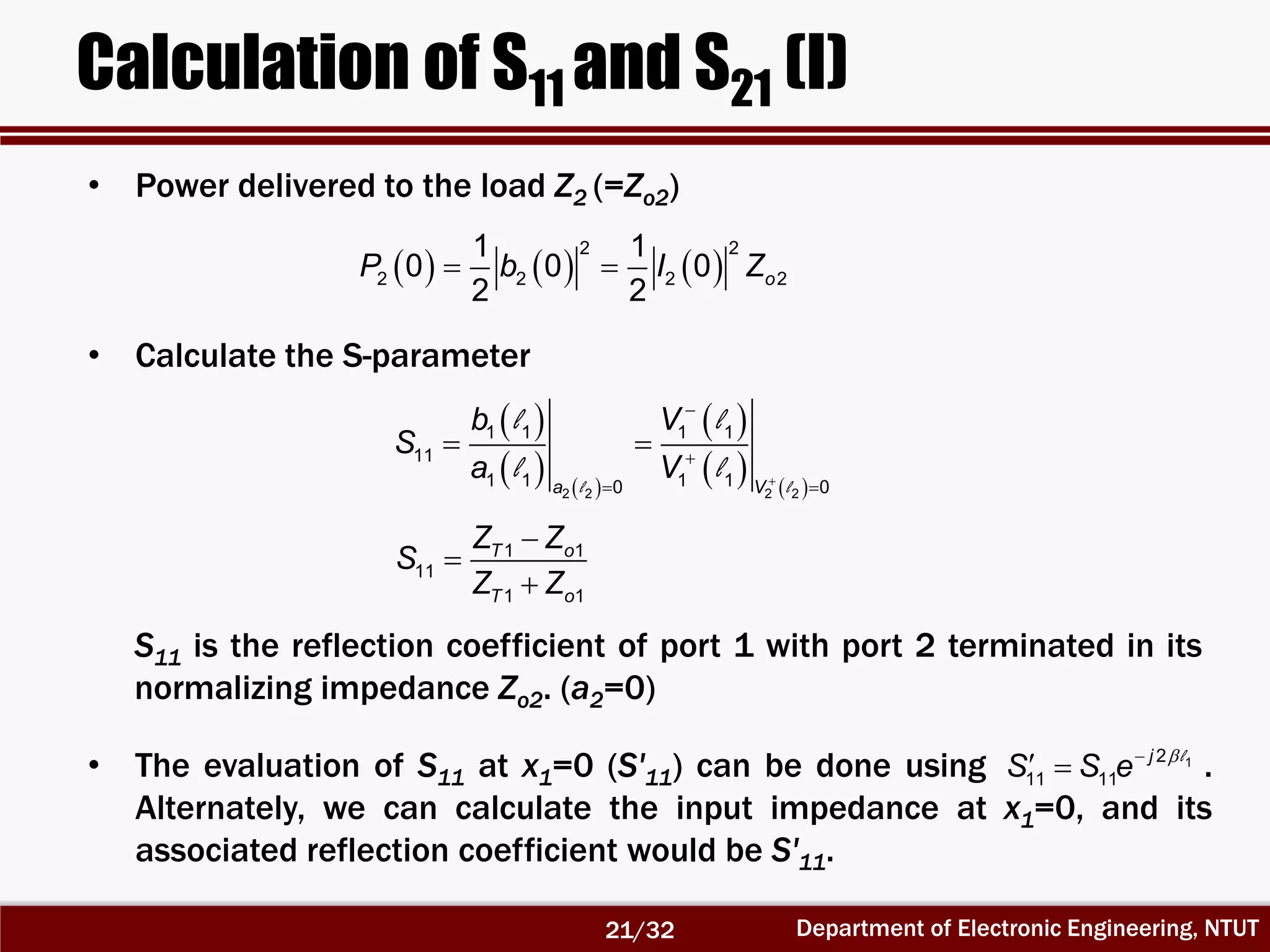
1 1 1 10 2,3, ,j
T o
T oa j n
b Z Z
S
a Z Z
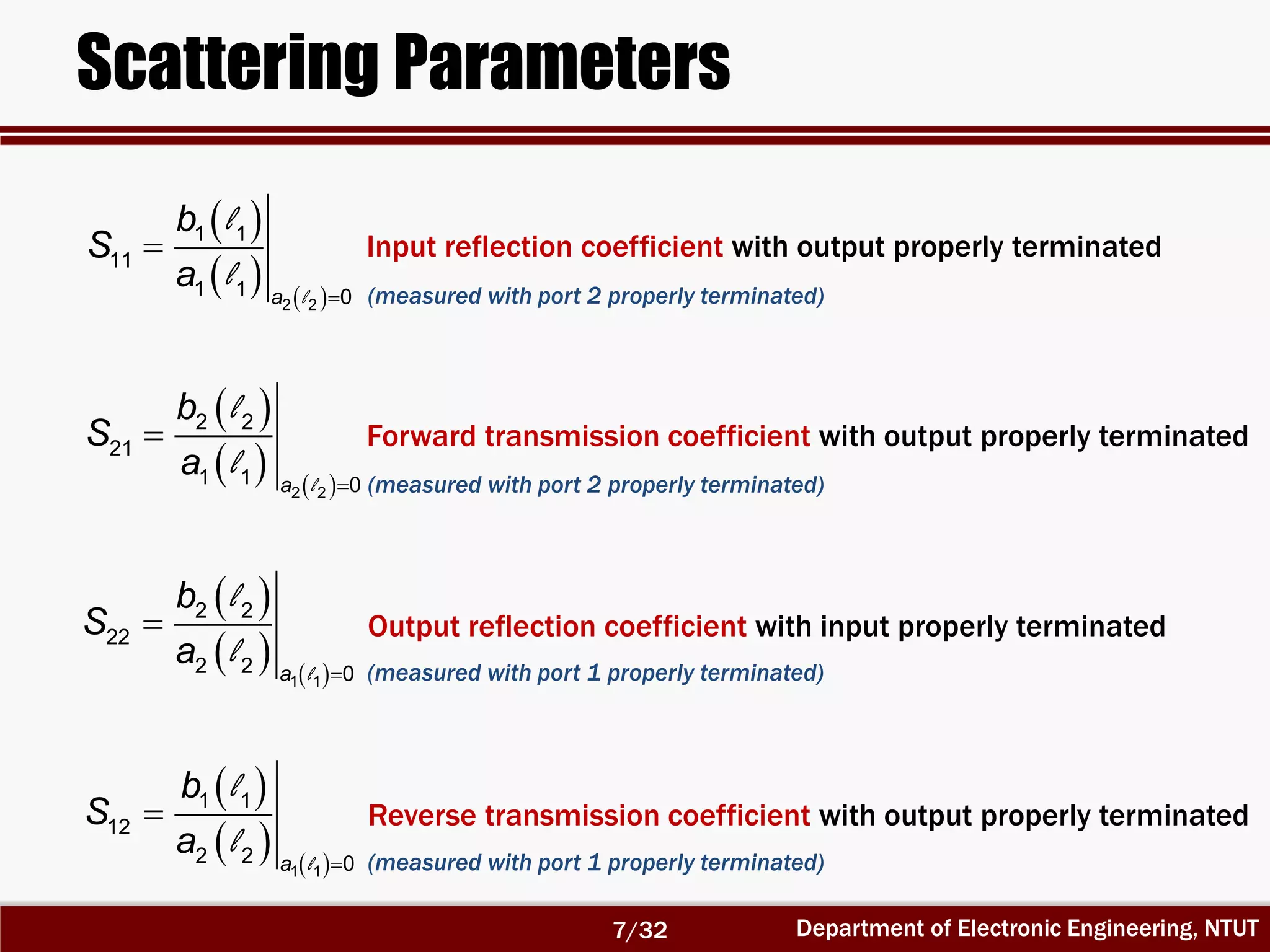
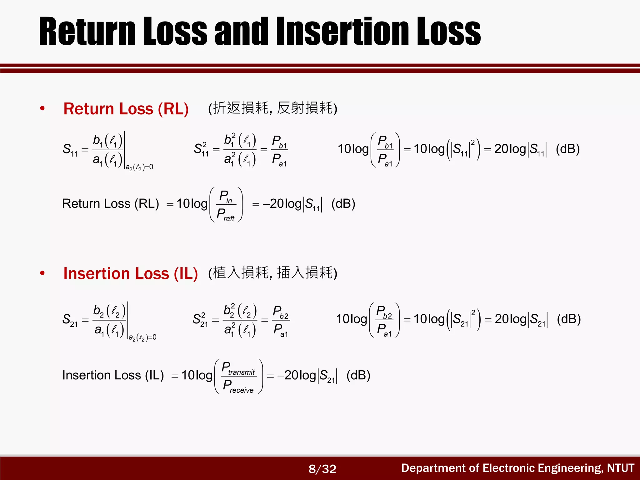
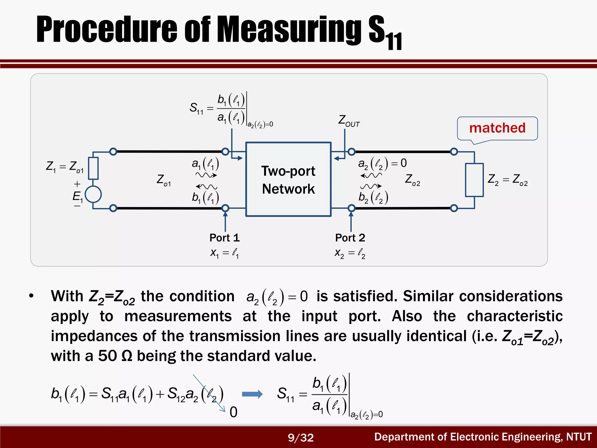
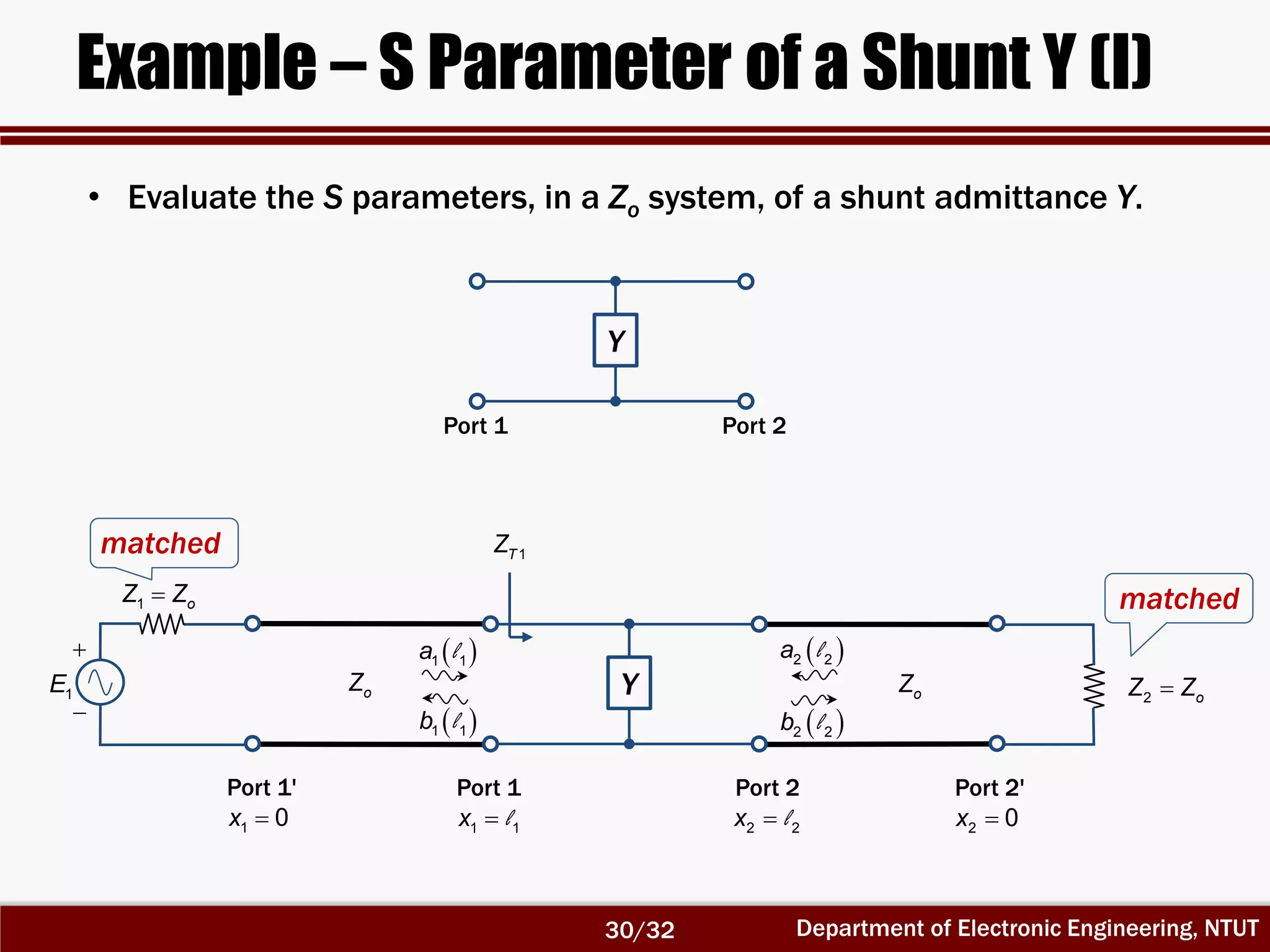
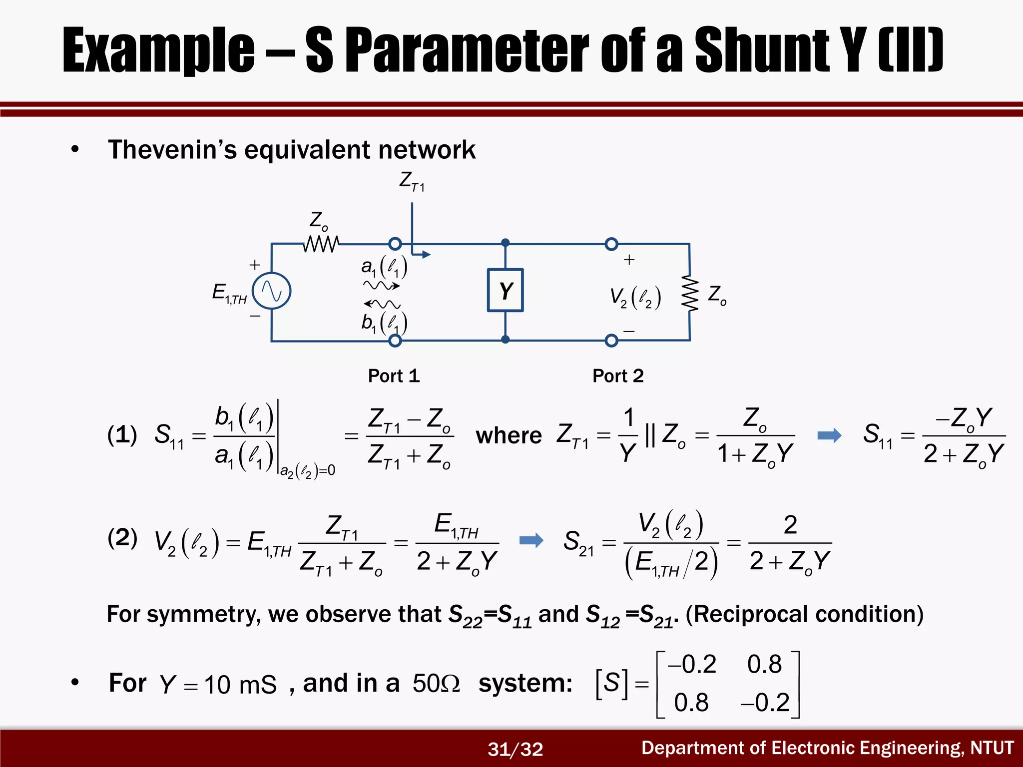
The S parameters of the n-port networks are easily measured.
For example S11 at x1=l1 is given by
where ZT1 is the impedance seen at port 1 with the other ports matched.
11/32](https://image.slidesharecdn.com/ch3-1-150613064402-lva1-app6892/75/RF-Circuit-Design-Ch3-1-Microwave-Network-11-2048.jpg)
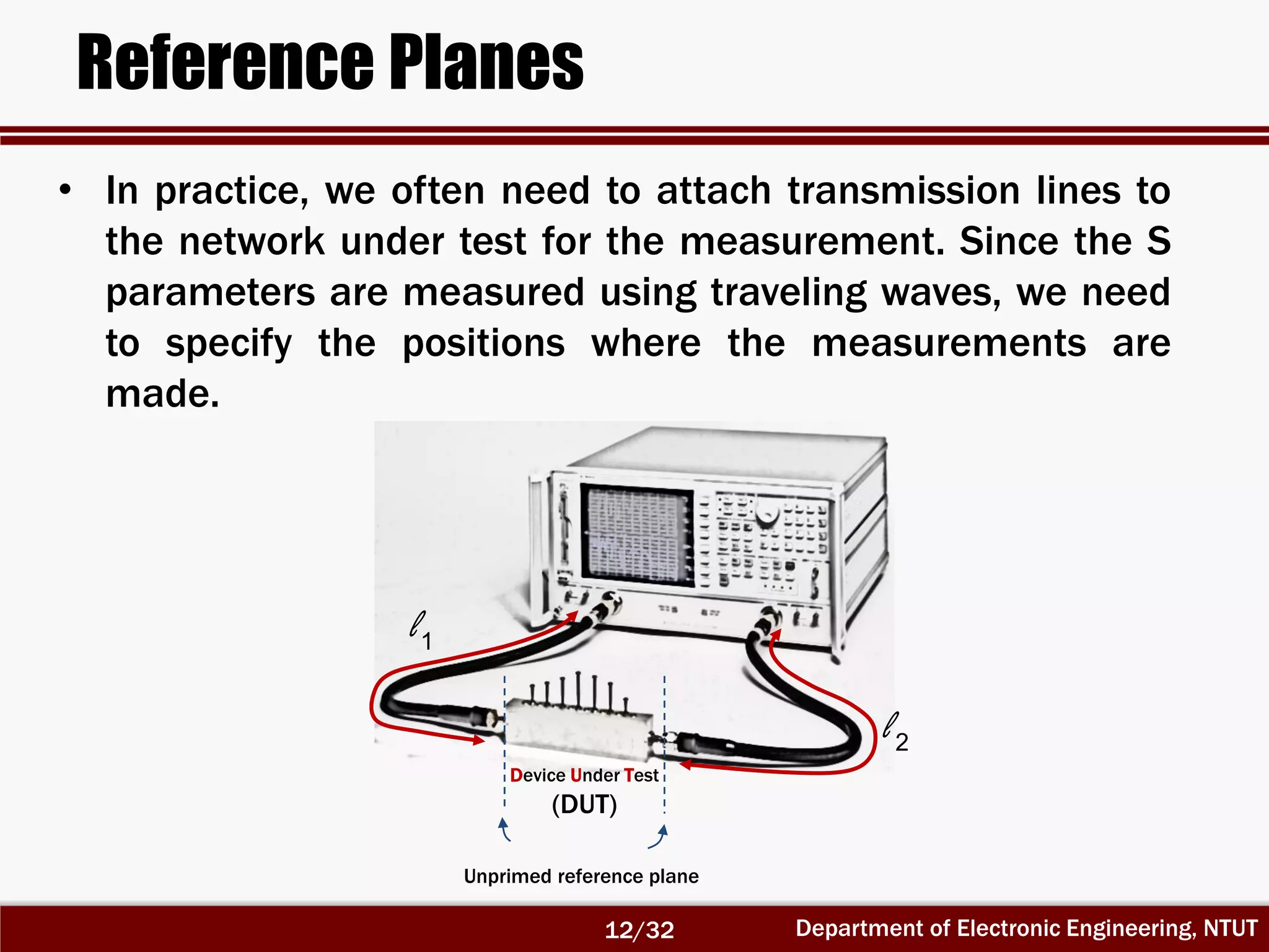

The document discusses the scattering matrix and microwave networks, detailing the concepts of traveling waves, normalized incident and reflected waves, and the use of two-port and n-port networks. It introduces key parameters such as reflection coefficients, transmission coefficients, return loss, and insertion loss alongside measurement procedures. Additionally, it emphasizes the importance of reference planes in practical measurements of the S-parameters.
![RF Circuit Design - [Ch3-2] Power Waves and Power-Gain Expressions](https://cdn.slidesharecdn.com/ss_thumbnails/ch3-2-150613064404-lva1-app6891-thumbnail.jpg?width=640&height=640&fit=bounds)
![RF Circuit Design - [Ch2-2] Smith Chart](https://cdn.slidesharecdn.com/ss_thumbnails/ch2-2-150613064401-lva1-app6891-thumbnail.jpg?width=640&height=640&fit=bounds)
![RF Circuit Design - [Ch2-1] Resonator and Impedance Matching](https://cdn.slidesharecdn.com/ss_thumbnails/ch2-1-150613064353-lva1-app6892-thumbnail.jpg?width=640&height=640&fit=bounds)
![RF Module Design - [Chapter 5] Low Noise Amplifier](https://cdn.slidesharecdn.com/ss_thumbnails/rfch5-150613070346-lva1-app6891-thumbnail.jpg?width=640&height=640&fit=bounds)
![RF Circuit Design - [Ch1-2] Transmission Line Theory](https://cdn.slidesharecdn.com/ss_thumbnails/ch1-2-150613064349-lva1-app6892-thumbnail.jpg?width=640&height=640&fit=bounds)
![RF Circuit Design - [Ch4-1] Microwave Transistor Amplifier](https://cdn.slidesharecdn.com/ss_thumbnails/ch4-1-150613064409-lva1-app6892-thumbnail.jpg?width=640&height=640&fit=bounds)
![RF Module Design - [Chapter 1] From Basics to RF Transceivers](https://cdn.slidesharecdn.com/ss_thumbnails/rfch1-150613070344-lva1-app6892-thumbnail.jpg?width=640&height=640&fit=bounds)

![RF Module Design - [Chapter 7] Voltage-Controlled Oscillator](https://cdn.slidesharecdn.com/ss_thumbnails/rfch7-150613070347-lva1-app6892-thumbnail.jpg?width=640&height=640&fit=bounds)
![RF Circuit Design - [Ch4-2] LNA, PA, and Broadband Amplifier](https://cdn.slidesharecdn.com/ss_thumbnails/ch4-2-150613064410-lva1-app6891-thumbnail.jpg?width=640&height=640&fit=bounds)
![Circuit Network Analysis - [Chapter1] Basic Circuit Laws](https://cdn.slidesharecdn.com/ss_thumbnails/ch1-150613063856-lva1-app6892-thumbnail.jpg?width=640&height=640&fit=bounds)
![Multiband Transceivers - [Chapter 1]](https://cdn.slidesharecdn.com/ss_thumbnails/ch1-150613070932-lva1-app6891-thumbnail.jpg?width=640&height=640&fit=bounds)
![RF Module Design - [Chapter 6] Power Amplifier](https://cdn.slidesharecdn.com/ss_thumbnails/rfch6-150613070347-lva1-app6891-thumbnail.jpg?width=640&height=640&fit=bounds)
![RF Module Design - [Chapter 4] Transceiver Architecture](https://cdn.slidesharecdn.com/ss_thumbnails/rfch4-150613070346-lva1-app6891-thumbnail.jpg?width=640&height=640&fit=bounds)
![射頻電子 - [第三章] 史密斯圖與阻抗匹配](https://cdn.slidesharecdn.com/ss_thumbnails/ch3-150613065103-lva1-app6892-thumbnail.jpg?width=640&height=640&fit=bounds)
![射頻電子 - [第五章] 射頻放大器設計](https://cdn.slidesharecdn.com/ss_thumbnails/ch5-150613065105-lva1-app6892-thumbnail.jpg?width=640&height=640&fit=bounds)
![射頻電子 - [第一章] 知識回顧與通訊系統簡介](https://cdn.slidesharecdn.com/ss_thumbnails/ch1-150613065058-lva1-app6891-thumbnail.jpg?width=640&height=640&fit=bounds)
![Multiband Transceivers - [Chapter 4] Design Parameters of Wireless Radios](https://cdn.slidesharecdn.com/ss_thumbnails/ch4-150613070934-lva1-app6892-thumbnail.jpg?width=640&height=640&fit=bounds)
![射頻電子實驗手冊 [實驗1 ~ 5] ADS入門, 傳輸線模擬, 直流模擬, 暫態模擬, 交流模擬](https://cdn.slidesharecdn.com/ss_thumbnails/simlab15-150613072411-lva1-app6892-thumbnail.jpg?width=640&height=640&fit=bounds)

![RF Module Design - [Chapter 2] Noises](https://cdn.slidesharecdn.com/ss_thumbnails/rfch2-150613070344-lva1-app6892-thumbnail.jpg?width=640&height=640&fit=bounds)
![RF Module Design - [Chapter 3] Linearity](https://cdn.slidesharecdn.com/ss_thumbnails/rfch3-150613070345-lva1-app6891-thumbnail.jpg?width=640&height=640&fit=bounds)
![射頻電子 - [實驗第一章] 基頻放大器設計](https://cdn.slidesharecdn.com/ss_thumbnails/e1-150613065108-lva1-app6892-thumbnail.jpg?width=640&height=640&fit=bounds)

![Multiband Transceivers - [Chapter 3] Basic Concept of Comm. Systems](https://cdn.slidesharecdn.com/ss_thumbnails/ch3-150613070933-lva1-app6892-thumbnail.jpg?width=640&height=640&fit=bounds)


![RF Circuit Design - [Ch1-1] Sinusoidal Steady-state Analysis](https://cdn.slidesharecdn.com/ss_thumbnails/ch1-1-150613064348-lva1-app6891-thumbnail.jpg?width=640&height=640&fit=bounds)
![Circuit Network Analysis - [Chapter2] Sinusoidal Steady-state Analysis](https://cdn.slidesharecdn.com/ss_thumbnails/ch2-150613063856-lva1-app6892-thumbnail.jpg?width=640&height=640&fit=bounds)
![射頻電子 - [第六章] 低雜訊放大器設計](https://cdn.slidesharecdn.com/ss_thumbnails/ch6-150613065106-lva1-app6892-thumbnail.jpg?width=640&height=640&fit=bounds)
![射頻電子 - [第四章] 散射參數網路](https://cdn.slidesharecdn.com/ss_thumbnails/ch4-150613065103-lva1-app6891-thumbnail.jpg?width=640&height=640&fit=bounds)
![Circuit Network Analysis - [Chapter4] Laplace Transform](https://cdn.slidesharecdn.com/ss_thumbnails/ch4-150613063858-lva1-app6891-thumbnail.jpg?width=640&height=640&fit=bounds)
![射頻電子 - [第二章] 傳輸線理論](https://cdn.slidesharecdn.com/ss_thumbnails/ch2-150613065059-lva1-app6891-thumbnail.jpg?width=640&height=640&fit=bounds)
![電路學 - [第六章] 二階RLC電路](https://cdn.slidesharecdn.com/ss_thumbnails/circuitch6-150613063009-lva1-app6892-thumbnail.jpg?width=640&height=640&fit=bounds)
![Circuit Network Analysis - [Chapter5] Transfer function, frequency response, ...](https://cdn.slidesharecdn.com/ss_thumbnails/ch5-150613063859-lva1-app6891-thumbnail.jpg?width=640&height=640&fit=bounds)
![電路學 - [第四章] 儲能元件](https://cdn.slidesharecdn.com/ss_thumbnails/circuitch4-150613063008-lva1-app6891-thumbnail.jpg?width=640&height=640&fit=bounds)
![電路學 - [第八章] 磁耦合電路](https://cdn.slidesharecdn.com/ss_thumbnails/circuitch8-150613063010-lva1-app6892-thumbnail.jpg?width=640&height=640&fit=bounds)
![Circuit Network Analysis - [Chapter3] Fourier Analysis](https://cdn.slidesharecdn.com/ss_thumbnails/ch3-150613063858-lva1-app6891-thumbnail.jpg?width=640&height=640&fit=bounds)
![電路學 - [第七章] 正弦激勵, 相量與穩態分析](https://cdn.slidesharecdn.com/ss_thumbnails/circuitch7-150613063009-lva1-app6891-thumbnail.jpg?width=640&height=640&fit=bounds)
![電路學 - [第三章] 網路定理](https://cdn.slidesharecdn.com/ss_thumbnails/circuitch3-150613063007-lva1-app6892-thumbnail.jpg?width=640&height=640&fit=bounds)
![電路學 - [第五章] 一階RC/RL電路](https://cdn.slidesharecdn.com/ss_thumbnails/circuitch5-150613063008-lva1-app6891-thumbnail.jpg?width=640&height=640&fit=bounds)


![Agilent ADS 模擬手冊 [實習2] 放大器設計](https://cdn.slidesharecdn.com/ss_thumbnails/2adsamp-150613072818-lva1-app6892-thumbnail.jpg?width=640&height=640&fit=bounds)
![射頻電子實驗手冊 - [實驗7] 射頻放大器模擬](https://cdn.slidesharecdn.com/ss_thumbnails/simlab7-150613072420-lva1-app6892-thumbnail.jpg?width=640&height=640&fit=bounds)
![Multiband Transceivers - [Chapter 6] Multi-mode and Multi-band Transceivers](https://cdn.slidesharecdn.com/ss_thumbnails/ch6-150613070935-lva1-app6891-thumbnail.jpg?width=640&height=640&fit=bounds)
![Multiband Transceivers - [Chapter 7] Multi-mode/Multi-band GSM/GPRS/TDMA/AMP...](https://cdn.slidesharecdn.com/ss_thumbnails/ch7-150613070936-lva1-app6892-thumbnail.jpg?width=640&height=640&fit=bounds)

![Agilent ADS 模擬手冊 [實習3] 壓控振盪器模擬](https://cdn.slidesharecdn.com/ss_thumbnails/3adsosc-150613072819-lva1-app6892-thumbnail.jpg?width=640&height=640&fit=bounds)

![射頻電子實驗手冊 [實驗6] 阻抗匹配模擬](https://cdn.slidesharecdn.com/ss_thumbnails/simlab6-150613072411-lva1-app6892-thumbnail.jpg?width=640&height=640&fit=bounds)
![Agilent ADS 模擬手冊 [實習1] 基本操作與射頻放大器設計](https://cdn.slidesharecdn.com/ss_thumbnails/1adsbasics-150613072812-lva1-app6891-thumbnail.jpg?width=640&height=640&fit=bounds)
![射頻電子實驗手冊 - [實驗8] 低雜訊放大器模擬](https://cdn.slidesharecdn.com/ss_thumbnails/simlab8-150613072425-lva1-app6891-thumbnail.jpg?width=640&height=640&fit=bounds)

![[嵌入式系統] MCS-51 實驗 - 使用 IAR (3)](https://cdn.slidesharecdn.com/ss_thumbnails/mcs51iarpart3-150613071723-lva1-app6892-thumbnail.jpg?width=640&height=640&fit=bounds)
![[ZigBee 嵌入式系統] ZigBee 應用實作 - 使用 TI Z-Stack Firmware](https://cdn.slidesharecdn.com/ss_thumbnails/zigbeeappimplementation-150613072040-lva1-app6891-thumbnail.jpg?width=640&height=640&fit=bounds)
![[嵌入式系統] MCS-51 實驗 - 使用 IAR (2)](https://cdn.slidesharecdn.com/ss_thumbnails/mcs51iarpart2-150613071717-lva1-app6891-thumbnail.jpg?width=640&height=640&fit=bounds)
![Multiband Transceivers - [Chapter 7] Spec. Table](https://cdn.slidesharecdn.com/ss_thumbnails/ch7table-150613070936-lva1-app6892-thumbnail.jpg?width=640&height=640&fit=bounds)
![[嵌入式系統] MCS-51 實驗 - 使用 IAR (1)](https://cdn.slidesharecdn.com/ss_thumbnails/mcs51iarpart1-150613071712-lva1-app6892-thumbnail.jpg?width=640&height=640&fit=bounds)
![[ZigBee 嵌入式系統] ZigBee Architecture 與 TI Z-Stack Firmware](https://cdn.slidesharecdn.com/ss_thumbnails/zigbeearchitecture-150613072045-lva1-app6892-thumbnail.jpg?width=640&height=640&fit=bounds)

![[嵌入式系統] 嵌入式系統進階](https://cdn.slidesharecdn.com/ss_thumbnails/advembedded-150613071653-lva1-app6892-thumbnail.jpg?width=640&height=640&fit=bounds)

![Seller Deck - Presentation [Concert L2].PPTX](https://cdn.slidesharecdn.com/ss_thumbnails/sellerdeck-presentationconcertl2-251219171156-24982daf-thumbnail.jpg?width=640&height=640&fit=bounds)


