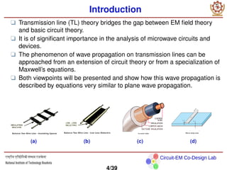
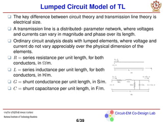
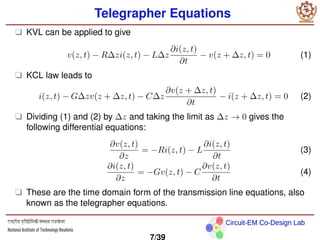
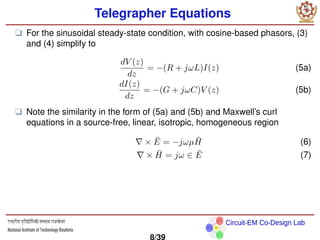
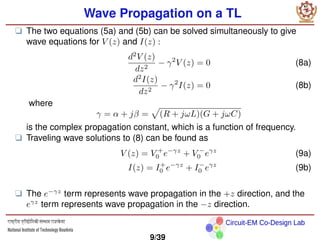
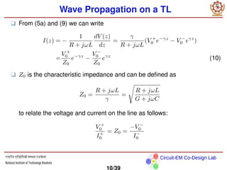
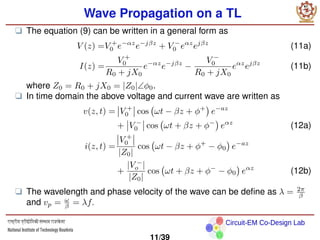
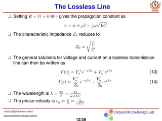
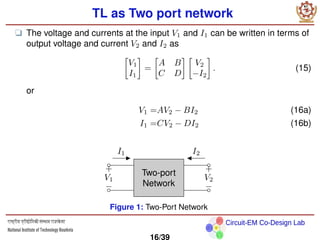
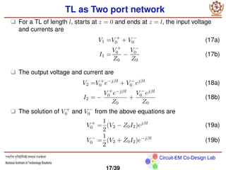
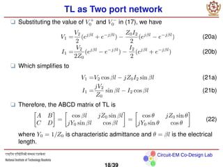
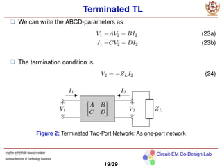
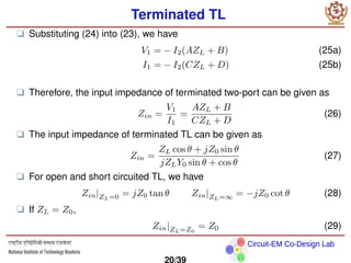
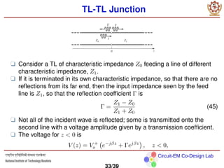
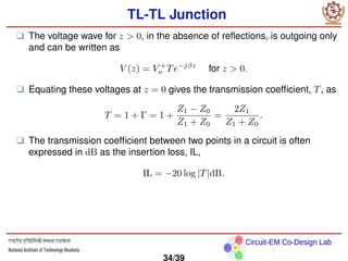
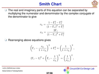
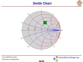
National Institute of Technology
Rourkela
Transmission Line Theory
EE3004 : Electromagnetic Field Theory
Dr. Rakesh Sinha
(Assistant Professor)
Circuit and Electromagnetic Co-Design Lab at NITR
Department of Electrical Engineering
National Institute of Technology (NIT) Rourkela
March 10, 2023
Circuit-EM Co-Design Lab
Outline
1 Introduction
2 THE LUMPED-ELEMENT CIRCUIT MODEL OF TL
3 TL as Two port network
4 THE TERMINATED LOSSLESS TRANSMISSION LINE
5 Smith Chart or Reflection Chart
2/39
Circuit-EM Co-Design Lab
Introduction
3/39
Circuit-EM Co-Design Lab
Introduction
❑ Transmission line (TL) theory bridges the gap between EM field theory
and basic circuit theory.
❑ It is of significant importance in the analysis of microwave circuits and
devices.
❑ The phenomenon of wave propagation on transmission lines can be
approached from an extension of circuit theory or from a specialization of
Maxwell’s equations.
❑ Both viewpoints will be presented and show how this wave propagation is
described by equations very similar to plane wave propagation.
(a) (b) (c) (d)
4/39
Circuit-EM Co-Design Lab
THE LUMPED-ELEMENT CIRCUIT MODEL OF
TL
5/39
Circuit-EM Co-Design Lab
Lumped Circuit Model of TL
❑ The key difference between circuit theory and transmission line theory is
electrical size.
❑ A transmission line is a distributed- parameter network, where voltages
and currents can vary in magnitude and phase over its length.
❑ Ordinary circuit analysis deals with lumped elements, where voltage and
current do not vary appreciably over the physical dimension of the
elements.
❑ R = series resistance per unit length, for both
conductors, in Ω/m.
❑ L = series inductance per unit length, for both
conductors, in H/m.
❑ G = shunt conductance per unit length, in S/m.
❑ C = shunt capacitance per unit length, in F/m.
6/39
Circuit-EM Co-Design Lab
Telegrapher Equations
❑ KVL can be applied to give
v(z, t) − R∆zi(z, t) − L∆z
∂i(z, t)
∂t
− v(z + ∆z, t) = 0 (1)
❑ KCL law leads to
i(z, t) − G∆zv(z + ∆z, t) − C∆z
∂v(z + ∆z, t)
∂t
− i(z + ∆z, t) = 0 (2)
❑ Dividing (1) and (2) by ∆z and taking the limit as ∆z → 0 gives the
following differential equations:
∂v(z, t)
∂z
= −Ri(z, t) − L
∂i(z, t)
∂t
(3)
∂i(z, t)
∂z
= −Gv(z, t) − C
∂v(z, t)
∂t
(4)
❑ These are the time domain form of the transmission line equations, also
known as the telegrapher equations.
7/39
Circuit-EM Co-Design Lab
Telegrapher Equations
❑ For the sinusoidal steady-state condition, with cosine-based phasors, (3)
and (4) simplify to
dV (z)
dz
= −(R + jωL)I(z) (5a)
dI(z)
dz
= −(G + jωC)V (z) (5b)
❑ Note the similarity in the form of (5a) and (5b) and Maxwell’s curl
equations in a source-free, linear, isotropic, homogeneous region
∇ × Ē = −jωµH̄ (6)
∇ × H̄ = jω ∈ Ē (7)
8/39
Circuit-EM Co-Design Lab
Wave Propagation on a TL
❑ The two equations (5a) and (5b) can be solved simultaneously to give
wave equations for V (z) and I(z) :
d2
V (z)
dz2
− γ2
V (z) = 0 (8a)
d2
I(z)
dz2
− γ2
I(z) = 0 (8b)
where
γ = α + jβ =
p
(R + jωL)(G + jωC)
is the complex propagation constant, which is a function of frequency.
❑ Traveling wave solutions to (8) can be found as
V (z) = V +
0 e−γz
+ V −
0 eγz
(9a)
I(z) = I+
0 e−γz
+ I−
0 eγz
(9b)
❑ The e−γz
term represents wave propagation in the +z direction, and the
eγz
term represents wave propagation in the −z direction.
9/39
Circuit-EM Co-Design Lab
Wave Propagation on a TL
❑ From (5a) and (9) we can write
I(z) = −
1
R + jωL
dV (z)
dz
=
γ
R + jωL
(V +
0 e−γz
− V −
0 eγz
)
=
V +
0
Z0
e−γz
−
V −
0
Z0
eγz
(10)
❑ Z0 is the characteristic impedance and can be defined as
Z0 =
R + jωL
γ
=
s
R + jωL
G + jωC
to relate the voltage and current on the line as follows:
V +
0
I+
0
= Z0 =
−V −
0
I−
0
10/39
Circuit-EM Co-Design Lab
Wave Propagation on a TL
❑ The equation (9) can be written in a general form as
V (z) =V +
0 e−αz
e−jβz
+ V −
0 eαz
ejβz
(11a)
I(z) =
V +
0
R0 + jX0
e−αz
e−jβz
−
V −
0
R0 + jX0
eαz
ejβz
(11b)
where Z0 = R0 + jX0 = |Z0|∠ϕ0.
❑ In time domain the above voltage and current wave are written as
v(z, t) = V +
0 cos ωt − βz + ϕ+

e−az
+ V −
0 cos ωt + βz + ϕ−

eαz
(12a)
i(z, t) =
V +
0
|Z0|
cos ωt − βz + ϕ+
− ϕ0

e−az
+
|V −
o |
|Z0|
cos ωt + βz + ϕ−
− ϕ0

eαz
(12b)
❑ The wavelength and phase velocity of the wave can be define as λ = 2π
β
and vp = ω
β = λf.
11/39
Circuit-EM Co-Design Lab
The Lossless Line
❑ Setting R = G = 0 in γ gives the propagation constant as
γ = α + jβ = jω
√
LC
❑ The characteristic impedance Z0 reduces to
Z0 =
r
L
C
❑ The general solutions for voltage and current on a lossless transmission
line can then be written as
V (z) = V +
o e−jβz
+ V −
o ejβz
(13)
I(z) =
V +
o
Z0
e−jβz
−
V −
o
Z0
ejβz
. (14)
❑ The wavelength is λ = 2π
β = 2π
ω
√
LC
❑ The phase velocity is vp = ω
β = 1
√
LC
12/39
Circuit-EM Co-Design Lab
Distortion Less Line
❑ A distortionless line has no frequency and no delay distortion.
❑ For a distortionless the attenuation constant (α) and velocity of
propagation (v) should not be a function of frequency.
❑ β should be a direct function of frequency.
❑ The required condition for a distortionless line can be derived from the
expression of propagation constant (γ).
❑ Since,
γ = α + jβ =
p
(R + jωL)(G + jωC)
=
s
RG

1 +
jωL
R
 
1 +
jωC
G

If, then,
ωL
R
=
ωC
G
γ =
s
RG

1 +
jωL
R
2
=
√
RG

1 +
jωL
R

13/39
Circuit-EM Co-Design Lab
Distortion Less Line
❑
γ =
√
RG + jω
L
R
√
RG =
√
RG + jωL
r
G
R
so,
α =
√
RG . . . ( not function of ω)
β = ωL
q
G
R . . . ( direct proportional to frequency)
❑ Thus α and β satisfy required condition of distortionless transmission line
under assumption of
L
R
=
C
G
14/39
Circuit-EM Co-Design Lab
TL as Two port network
15/39
Circuit-EM Co-Design Lab
TL as Two port network
❑ The voltage and currents at the input V1 and I1 can be written in terms of
output voltage and current V2 and I2 as

V1
I1

=

A B
C D
 
V2
−I2

. (15)
or
V1 =AV2 − BI2 (16a)
I1 =CV2 − DI2 (16b)
Two-port
Network
I1
+
−
V1
I2
−
+
V2
Figure 1: Two-Port Network
16/39
Circuit-EM Co-Design Lab
TL as Two port network
❑ For a TL of length l, starts at z = 0 and ends at z = l, the input voltage
and currents are
V1 =V +
0 + V −
0 (17a)
I1 =
V +
0
Z0
−
V −
0
Z0
(17b)
❑ The output voltage and current are
V2 =V +
0 e−jβl
+ V −
0 ejβl
(18a)
I2 = −
V +
0 e−jβl
Z0
+
V −
0 ejβl
Z0
(18b)
❑ The solution of V +
0 and V −
0 from the above equations are
V +
0 =
1
2
(V2 − Z0I2)ejβl
(19a)
V −
0 =
1
2
(V2 + Z0I2)e−jβl
(19b)
17/39
Circuit-EM Co-Design Lab
TL as Two port network
❑ Substituting the value of V +
0 and V −
0 in (17), we have
V1 =
V2
2
(ejβl
+ e−jβl
) −
Z0I2
2
(ejβl
− e−jβl
) (20a)
I1 =
V2
2Z0
(ejβl
− e−jβl
) −
I2
2
(ejβl
+ e−jβl
) (20b)
❑ Which simplifies to
V1 =V2 cos βl − jZ0I2 sin βl (21a)
I1 =
jV2
Z0
sin βl − I2 cos βl (21b)
❑ Therefore, the ABCD matrix of TL is

A B
C D

=

cos βl jZ0 sin βl
jY0 sin βl cos βl

=

cos θ jZ0 sin θ
jY0 sin θ cos θ

(22)
where Y0 = 1/Z0 is characteristic admittance and θ = βl is the electrical
length.
18/39
Circuit-EM Co-Design Lab
Terminated TL
❑ We can write the ABCD-parameters as
V1 =AV2 − BI2 (23a)
I1 =CV2 − DI2 (23b)
❑ The termination condition is
V2 = −ZLI2 (24)

A B
C D

I1
+
−
V1
I2
−
+
V2 ZL
Figure 2: Terminated Two-Port Network: As one-port network
19/39
Circuit-EM Co-Design Lab
Terminated TL
❑ Substituting (24) into (23), we have
V1 = − I2(AZL + B) (25a)
I1 = − I2(CZL + D) (25b)
❑ Therefore, the input impedance of terminated two-port can be given as
Zin =
V1
I1
=
AZL + B
CZL + D
(26)
❑ The input impedance of terminated TL can be given as
Zin =
ZL cos θ + jZ0 sin θ
jZLY0 sin θ + cos θ
(27)
❑ For open and short circuited TL, we have
Zin|ZL=0 = jZ0 tan θ Zin|ZL=∞ = −jZ0 cot θ (28)
❑ If ZL = Z0,
Zin|ZL=Z0
= Z0 (29)
20/39
Circuit-EM Co-Design Lab
THE TERMINATED LOSSLESS TRANSMISSION
LINE
21/39
Circuit-EM Co-Design Lab
Terminated Lossless TL
❑ The total voltage on the line can be written as a sum of incident and
reflected waves:
V (z) = V +
0 e−jβz
+ V −
0 ejβz
(30)
❑ Similarly, the total current on the line is described by
I(z) =
V +
0
Z0
e−jβz
−
V −
0
Z0
ejβz
(31)
22/39
Circuit-EM Co-Design Lab
Terminated Lossless TL
❑ The total voltage and current at the load are related by the load
impedance, so at z = 0 we must have
ZL =
V (0)
I(0)
=
V +
0 + V −
0
V +
0 − V −
0
Z0 (32)
❑ Solving for V −
0 gives
V −
0 =
ZL − Z0
ZL + Z0
V +
0 (33)
❑ The amplitude of the reflected wave normalized to the amplitude of the
incident voltage wave is defined as the voltage reflection coefficient, Γ :
Γ =
V −
0
V +
0
=
ZL − Z0
ZL + Z0
(34)
❑ The total voltage and current waves on the line can then be written as
V (z) = V +
0 e−jβz
+ Γejβz

(35)
I(z) =
V +
0
Z0
e−jβz
− Γejβz

. (36)
23/39
Circuit-EM Co-Design Lab
Terminated Lossless TL
❑ The voltage and current on the line consist of a superposition of an
incident and a reflected wave; such waves are called standing waves.
❑ Only when Γ = 0 is there no reflected wave.
❑ To obtain Γ = 0, the load impedance ZL, must be equal to the
characteristic impedance Z0 of the TL.
❑ Such a load is said to be matched to the line since there is no reflection
of the incident wave.
❑ Now consider the time-average power flow along the line at the point z :
Pavg =
1
2
Re {V (z)I(z)∗
} =
1
2
V +
0
2
Z0
Re

1 − Γ∗
e−2jβz
+ Γe2jβz
− |Γ|2
=
1
2
|V +
o |
2
Z0
1 − |Γ|2

(37)
❑ The total power delivered to the load (Pavg) is equal to the incident power

V +
0
2
/2Z0

minus the reflected power

V +
0
2
|Γ|2
/2Z0

.
24/39
Circuit-EM Co-Design Lab
Return Loss
❑ When the load is mismatched, not all of the available power from the
generator is delivered to the load.
❑ This loss is called return loss (RL), and is defined (in dB ) as
RL = −20 log |Γ|dB
❑ So that a matched load (Γ = 0 ) has a return loss of ∞dB (no reflected
power), while a total reflection (|Γ| = 1 ) has a return loss of 0 dB (all
incident power is reflected).
❑ Note that return loss is a nonnegative number for reflection from a
passive network.
25/39
Circuit-EM Co-Design Lab
Standing Wave Ratio
❑ If the load is matched to the line, Γ = 0 and the magnitude of the voltage
on the line is |V (z)| = |V +
o |, which is a constant.
❑ When reflection is there
|V (z)| = V +
o 1 + Γe2jβz
= V +
o 1 + Γe−2jβl
= V +
o |1 + |Γ|ej(θ−2βl)
| (38)
❑ The maximum value occurs when the phase term ej(θ−2βl)
= 1 and is
given by
Vmax = V +
o (1 + |Γ|).
❑ The minimum value occurs when the phase term ej(θ−2βℓ)
= −1 and is
given by
Vmin = V +
o (1 − |Γ|).
❑ As |Γ| increases, the ratio of Vmax to Vmin increases, so a measure of the
mismatch of a line, called the standing wave ratio (SWR), can be defined
as
SWR =
Vmax
Vmin
=
1 + |Γ|
1 − |Γ|
.
26/39
Circuit-EM Co-Design Lab
Input Impedance
❑ At a distance l = −z from the load, the input impedance seen looking
toward the load is
Zin =
V (−ℓ)
I(−ℓ)
=
V +
o ejβℓ
+ Γe−jβℓ

V +
o (ejβℓ − Γe−jβℓ)
Z0 =
1 + Γe−2jβℓ
1 − Γe−2jβℓ
Z0
❑ A more usable form may be obtained by using Γ = (ZL − Z0)/(ZL + Z0)
Zin = Z0
(ZL + Z0) ejβℓ
+ (ZL − Z0) e−jβℓ
(ZL + Z0) ejβℓ − (ZL − Z0) e−jβℓ
= Z0
ZL cos βℓ + jZ0 sin βℓ
Z0 cos βℓ + jZL sin βℓ
= Z0
ZL + jZ0 tan βℓ
Z0 + jZL tan βℓ
= Z0
ZL cos βℓ + jZ0 sin βℓ
Z0 cos βℓ + jZL sin βℓ
.
27/39
Circuit-EM Co-Design Lab
Short Circuited TL
❑ Consider the TL circuit is terminated in a short circuit, ZL = 0.
❑ From Γ = (ZL − Z0)/(ZL + Z0), it is seen that the reflection coefficient for
a short circuit load is Γ = −1;
❑ It then follows from SWR = Vmax
Vmin
= 1+|Γ|
1−|Γ| that the standing wave ratio is
infinite.
❑ The voltage and current on the line are
V (z) = V +
o e−jβz
− ejβz

= −2jV +
o sin βz, (39)
I(z) =
V +
o
Z0
e−jβz
+ ejβz

=
2V +
o
Z0
cos βz. (40)
❑ The input impedance is Zin = jZ0 tan βℓ.
28/39
Circuit-EM Co-Design Lab
Short Circuited TL
29/39
Circuit-EM Co-Design Lab
Open Circuited TL
❑ Consider the open-circuited line with ZL = ∞ or YL = 0.
❑ From Γ = (ZL − Z0)/(ZL + Z0) = (1 − YLZ0)/(1 + YLZ0), it is seen that
the reflection coefficient for a open circuit load is Γ = 1.
❑ The standing wave ratio is again infinite.
❑ The voltage and current on the line are
V (z) = V +
o e−jβz
+ ejβz

= 2V +
o cos βz (41)
I(z) =
V +
o
Z0
e−jβz
− ejβz

=
−2jV +
o
Z0
sin βz (42)
❑ The input impedance is Zin = −jZ0 cot βℓ
30/39
Circuit-EM Co-Design Lab
Open Circuited TL
31/39
Circuit-EM Co-Design Lab
TL Terminated by Resistive load
❑ Consider the a TL is terminated by resistive load ZL = nZ0.
❑ From Γ = (ZL − Z0)/(ZL + Z0), it is seen that the reflection coefficient is
Γ = (n − 1)/(n + 1).
❑ The standing wave ratio is n if n  1 and 1/n if n  1.
❑ The voltage and current on the line are
V (z) =V +
o e−jβz
+ Γejβz

= V +
o ((1 + Γ) cos βz − j(1 − Γ) sin βz)
=
2V +
o
n + 1
(n cos βz − j sin βz) (43)
I(z) =
V +
o
Z0
e−jβz
− Γejβz

=
V +
o
Z0
((1 − Γ) cos βz − j(1 + Γ) sin βz)
=
2V +
o
(n + 1)Z0
(cos βz − jn sin βz) (44)
❑ The input impedance is Zin = Z0
n cos βℓ+j sin βℓ
cos βℓ+jn sin βℓ = Z0
n βl=π/2
= nZ0|βl=π
32/39
Circuit-EM Co-Design Lab
TL-TL Junction
❑ Consider a TL of characteristic impedance Z0 feeding a line of different
characteristic impedance, Z1.
❑ If it is terminated in its own characteristic impedance, so that there are no
reflections from its far end, then the input impedance seen by the feed
line is Z1, so that the reflection coefficient Γ is
Γ =
Z1 − Z0
Z1 + Z0
(45)
❑ Not all of the incident wave is reflected; some is transmitted onto the
second line with a voltage amplitude given by a transmission coefficient.
❑ The voltage for z  0 is
V (z) = V +
o e−jβz
+ Γejβz

, z  0,
33/39
Circuit-EM Co-Design Lab
TL-TL Junction
❑ The voltage wave for z  0, in the absence of reflections, is outgoing only
and can be written as
V (z) = V +
o Te−jβz
for z  0.
❑ Equating these voltages at z = 0 gives the transmission coefficient, T, as
T = 1 + Γ = 1 +
Z1 − Z0
Z1 + Z0
=
2Z1
Z1 + Z0
.
❑ The transmission coefficient between two points in a circuit is often
expressed in dB as the insertion loss, IL,
IL = −20 log |T|dB.
34/39
Circuit-EM Co-Design Lab
Smith Chart or Reflection Chart
35/39
Circuit-EM Co-Design Lab
Smith Chart
❑ If a lossless line of characteristic impedance Z0 is terminated with a load
impedance ZL, the reflection coefficient at the load can be written as
Γ =
zL − 1
zL + 1
= |Γ|ejθ
,
where zL = ZL/Z0 is the normalized load impedance.
❑ This relation can be solved for zL in terms of Γ to give
zL =
1 + |Γ|ejθ
1 − |Γ|ejθ
❑ This complex equation can be reduced to two real equations by writing Γ
and zL in terms of their real and imaginary parts, Γ = Γr + jΓi, and
zL = rL + jxL, giving
rL + jxL =
(1 + Γr) + jΓi
(1 − Γr) − jΓi
.
36/39
Circuit-EM Co-Design Lab
Smith Chart
❑ The real and imaginary parts of this equation can be separated by
multiplying the numerator and denominator by the complex conjugate of
the denominator to give
rL =
1 − Γ2
r − Γ2
i
(1 − Γr)
2
+ Γ2
i
xL =
2Γi
(1 − Γr)
2
+ Γ2
i
❑ Rearranging above equations gives

Γr −
rL
1 + rL
2
+ Γ2
i =

1
1 + rL
2
,
(Γr − 1)
2
+

Γi −
1
xL
2
=

1
xL
2
,
37/39
Circuit-EM Co-Design Lab
Smith Chart
38/39
National Institute of Technology
Rourkela
Thanks.

TL_Theory.pdf

  • 1.
    National Institute ofTechnology Rourkela Transmission Line Theory EE3004 : Electromagnetic Field Theory Dr. Rakesh Sinha (Assistant Professor) Circuit and Electromagnetic Co-Design Lab at NITR Department of Electrical Engineering National Institute of Technology (NIT) Rourkela March 10, 2023
  • 2.
    Circuit-EM Co-Design Lab Outline 1Introduction 2 THE LUMPED-ELEMENT CIRCUIT MODEL OF TL 3 TL as Two port network 4 THE TERMINATED LOSSLESS TRANSMISSION LINE 5 Smith Chart or Reflection Chart 2/39
  • 3.
  • 4.
    Circuit-EM Co-Design Lab Introduction ❑Transmission line (TL) theory bridges the gap between EM field theory and basic circuit theory. ❑ It is of significant importance in the analysis of microwave circuits and devices. ❑ The phenomenon of wave propagation on transmission lines can be approached from an extension of circuit theory or from a specialization of Maxwell’s equations. ❑ Both viewpoints will be presented and show how this wave propagation is described by equations very similar to plane wave propagation. (a) (b) (c) (d) 4/39
  • 5.
    Circuit-EM Co-Design Lab THELUMPED-ELEMENT CIRCUIT MODEL OF TL 5/39
  • 6.
    Circuit-EM Co-Design Lab LumpedCircuit Model of TL ❑ The key difference between circuit theory and transmission line theory is electrical size. ❑ A transmission line is a distributed- parameter network, where voltages and currents can vary in magnitude and phase over its length. ❑ Ordinary circuit analysis deals with lumped elements, where voltage and current do not vary appreciably over the physical dimension of the elements. ❑ R = series resistance per unit length, for both conductors, in Ω/m. ❑ L = series inductance per unit length, for both conductors, in H/m. ❑ G = shunt conductance per unit length, in S/m. ❑ C = shunt capacitance per unit length, in F/m. 6/39
  • 7.
    Circuit-EM Co-Design Lab TelegrapherEquations ❑ KVL can be applied to give v(z, t) − R∆zi(z, t) − L∆z ∂i(z, t) ∂t − v(z + ∆z, t) = 0 (1) ❑ KCL law leads to i(z, t) − G∆zv(z + ∆z, t) − C∆z ∂v(z + ∆z, t) ∂t − i(z + ∆z, t) = 0 (2) ❑ Dividing (1) and (2) by ∆z and taking the limit as ∆z → 0 gives the following differential equations: ∂v(z, t) ∂z = −Ri(z, t) − L ∂i(z, t) ∂t (3) ∂i(z, t) ∂z = −Gv(z, t) − C ∂v(z, t) ∂t (4) ❑ These are the time domain form of the transmission line equations, also known as the telegrapher equations. 7/39
  • 8.
    Circuit-EM Co-Design Lab TelegrapherEquations ❑ For the sinusoidal steady-state condition, with cosine-based phasors, (3) and (4) simplify to dV (z) dz = −(R + jωL)I(z) (5a) dI(z) dz = −(G + jωC)V (z) (5b) ❑ Note the similarity in the form of (5a) and (5b) and Maxwell’s curl equations in a source-free, linear, isotropic, homogeneous region ∇ × Ē = −jωµH̄ (6) ∇ × H̄ = jω ∈ Ē (7) 8/39
  • 9.
    Circuit-EM Co-Design Lab WavePropagation on a TL ❑ The two equations (5a) and (5b) can be solved simultaneously to give wave equations for V (z) and I(z) : d2 V (z) dz2 − γ2 V (z) = 0 (8a) d2 I(z) dz2 − γ2 I(z) = 0 (8b) where γ = α + jβ = p (R + jωL)(G + jωC) is the complex propagation constant, which is a function of frequency. ❑ Traveling wave solutions to (8) can be found as V (z) = V + 0 e−γz + V − 0 eγz (9a) I(z) = I+ 0 e−γz + I− 0 eγz (9b) ❑ The e−γz term represents wave propagation in the +z direction, and the eγz term represents wave propagation in the −z direction. 9/39
  • 10.
    Circuit-EM Co-Design Lab WavePropagation on a TL ❑ From (5a) and (9) we can write I(z) = − 1 R + jωL dV (z) dz = γ R + jωL (V + 0 e−γz − V − 0 eγz ) = V + 0 Z0 e−γz − V − 0 Z0 eγz (10) ❑ Z0 is the characteristic impedance and can be defined as Z0 = R + jωL γ = s R + jωL G + jωC to relate the voltage and current on the line as follows: V + 0 I+ 0 = Z0 = −V − 0 I− 0 10/39
  • 11.
    Circuit-EM Co-Design Lab WavePropagation on a TL ❑ The equation (9) can be written in a general form as V (z) =V + 0 e−αz e−jβz + V − 0 eαz ejβz (11a) I(z) = V + 0 R0 + jX0 e−αz e−jβz − V − 0 R0 + jX0 eαz ejβz (11b) where Z0 = R0 + jX0 = |Z0|∠ϕ0. ❑ In time domain the above voltage and current wave are written as v(z, t) = V + 0 cos ωt − βz + ϕ+ e−az + V − 0 cos ωt + βz + ϕ− eαz (12a) i(z, t) = V + 0 |Z0| cos ωt − βz + ϕ+ − ϕ0 e−az + |V − o | |Z0| cos ωt + βz + ϕ− − ϕ0 eαz (12b) ❑ The wavelength and phase velocity of the wave can be define as λ = 2π β and vp = ω β = λf. 11/39
  • 12.
    Circuit-EM Co-Design Lab TheLossless Line ❑ Setting R = G = 0 in γ gives the propagation constant as γ = α + jβ = jω √ LC ❑ The characteristic impedance Z0 reduces to Z0 = r L C ❑ The general solutions for voltage and current on a lossless transmission line can then be written as V (z) = V + o e−jβz + V − o ejβz (13) I(z) = V + o Z0 e−jβz − V − o Z0 ejβz . (14) ❑ The wavelength is λ = 2π β = 2π ω √ LC ❑ The phase velocity is vp = ω β = 1 √ LC 12/39
  • 13.
    Circuit-EM Co-Design Lab DistortionLess Line ❑ A distortionless line has no frequency and no delay distortion. ❑ For a distortionless the attenuation constant (α) and velocity of propagation (v) should not be a function of frequency. ❑ β should be a direct function of frequency. ❑ The required condition for a distortionless line can be derived from the expression of propagation constant (γ). ❑ Since, γ = α + jβ = p (R + jωL)(G + jωC) = s RG 1 + jωL R 1 + jωC G If, then, ωL R = ωC G γ = s RG 1 + jωL R 2 = √ RG 1 + jωL R 13/39
  • 14.
    Circuit-EM Co-Design Lab DistortionLess Line ❑ γ = √ RG + jω L R √ RG = √ RG + jωL r G R so, α = √ RG . . . ( not function of ω) β = ωL q G R . . . ( direct proportional to frequency) ❑ Thus α and β satisfy required condition of distortionless transmission line under assumption of L R = C G 14/39
  • 15.
    Circuit-EM Co-Design Lab TLas Two port network 15/39
  • 16.
    Circuit-EM Co-Design Lab TLas Two port network ❑ The voltage and currents at the input V1 and I1 can be written in terms of output voltage and current V2 and I2 as V1 I1 = A B C D V2 −I2 . (15) or V1 =AV2 − BI2 (16a) I1 =CV2 − DI2 (16b) Two-port Network I1 + − V1 I2 − + V2 Figure 1: Two-Port Network 16/39
  • 17.
    Circuit-EM Co-Design Lab TLas Two port network ❑ For a TL of length l, starts at z = 0 and ends at z = l, the input voltage and currents are V1 =V + 0 + V − 0 (17a) I1 = V + 0 Z0 − V − 0 Z0 (17b) ❑ The output voltage and current are V2 =V + 0 e−jβl + V − 0 ejβl (18a) I2 = − V + 0 e−jβl Z0 + V − 0 ejβl Z0 (18b) ❑ The solution of V + 0 and V − 0 from the above equations are V + 0 = 1 2 (V2 − Z0I2)ejβl (19a) V − 0 = 1 2 (V2 + Z0I2)e−jβl (19b) 17/39
  • 18.
    Circuit-EM Co-Design Lab TLas Two port network ❑ Substituting the value of V + 0 and V − 0 in (17), we have V1 = V2 2 (ejβl + e−jβl ) − Z0I2 2 (ejβl − e−jβl ) (20a) I1 = V2 2Z0 (ejβl − e−jβl ) − I2 2 (ejβl + e−jβl ) (20b) ❑ Which simplifies to V1 =V2 cos βl − jZ0I2 sin βl (21a) I1 = jV2 Z0 sin βl − I2 cos βl (21b) ❑ Therefore, the ABCD matrix of TL is A B C D = cos βl jZ0 sin βl jY0 sin βl cos βl = cos θ jZ0 sin θ jY0 sin θ cos θ (22) where Y0 = 1/Z0 is characteristic admittance and θ = βl is the electrical length. 18/39
  • 19.
    Circuit-EM Co-Design Lab TerminatedTL ❑ We can write the ABCD-parameters as V1 =AV2 − BI2 (23a) I1 =CV2 − DI2 (23b) ❑ The termination condition is V2 = −ZLI2 (24) A B C D I1 + − V1 I2 − + V2 ZL Figure 2: Terminated Two-Port Network: As one-port network 19/39
  • 20.
    Circuit-EM Co-Design Lab TerminatedTL ❑ Substituting (24) into (23), we have V1 = − I2(AZL + B) (25a) I1 = − I2(CZL + D) (25b) ❑ Therefore, the input impedance of terminated two-port can be given as Zin = V1 I1 = AZL + B CZL + D (26) ❑ The input impedance of terminated TL can be given as Zin = ZL cos θ + jZ0 sin θ jZLY0 sin θ + cos θ (27) ❑ For open and short circuited TL, we have Zin|ZL=0 = jZ0 tan θ Zin|ZL=∞ = −jZ0 cot θ (28) ❑ If ZL = Z0, Zin|ZL=Z0 = Z0 (29) 20/39
  • 21.
    Circuit-EM Co-Design Lab THETERMINATED LOSSLESS TRANSMISSION LINE 21/39
  • 22.
    Circuit-EM Co-Design Lab TerminatedLossless TL ❑ The total voltage on the line can be written as a sum of incident and reflected waves: V (z) = V + 0 e−jβz + V − 0 ejβz (30) ❑ Similarly, the total current on the line is described by I(z) = V + 0 Z0 e−jβz − V − 0 Z0 ejβz (31) 22/39
  • 23.
    Circuit-EM Co-Design Lab TerminatedLossless TL ❑ The total voltage and current at the load are related by the load impedance, so at z = 0 we must have ZL = V (0) I(0) = V + 0 + V − 0 V + 0 − V − 0 Z0 (32) ❑ Solving for V − 0 gives V − 0 = ZL − Z0 ZL + Z0 V + 0 (33) ❑ The amplitude of the reflected wave normalized to the amplitude of the incident voltage wave is defined as the voltage reflection coefficient, Γ : Γ = V − 0 V + 0 = ZL − Z0 ZL + Z0 (34) ❑ The total voltage and current waves on the line can then be written as V (z) = V + 0 e−jβz + Γejβz (35) I(z) = V + 0 Z0 e−jβz − Γejβz . (36) 23/39
  • 24.
    Circuit-EM Co-Design Lab TerminatedLossless TL ❑ The voltage and current on the line consist of a superposition of an incident and a reflected wave; such waves are called standing waves. ❑ Only when Γ = 0 is there no reflected wave. ❑ To obtain Γ = 0, the load impedance ZL, must be equal to the characteristic impedance Z0 of the TL. ❑ Such a load is said to be matched to the line since there is no reflection of the incident wave. ❑ Now consider the time-average power flow along the line at the point z : Pavg = 1 2 Re {V (z)I(z)∗ } = 1 2 V + 0 2 Z0 Re 1 − Γ∗ e−2jβz + Γe2jβz − |Γ|2 = 1 2 |V + o | 2 Z0 1 − |Γ|2 (37) ❑ The total power delivered to the load (Pavg) is equal to the incident power V + 0 2 /2Z0 minus the reflected power V + 0 2 |Γ|2 /2Z0 . 24/39
  • 25.
    Circuit-EM Co-Design Lab ReturnLoss ❑ When the load is mismatched, not all of the available power from the generator is delivered to the load. ❑ This loss is called return loss (RL), and is defined (in dB ) as RL = −20 log |Γ|dB ❑ So that a matched load (Γ = 0 ) has a return loss of ∞dB (no reflected power), while a total reflection (|Γ| = 1 ) has a return loss of 0 dB (all incident power is reflected). ❑ Note that return loss is a nonnegative number for reflection from a passive network. 25/39
  • 26.
    Circuit-EM Co-Design Lab StandingWave Ratio ❑ If the load is matched to the line, Γ = 0 and the magnitude of the voltage on the line is |V (z)| = |V + o |, which is a constant. ❑ When reflection is there |V (z)| = V + o 1 + Γe2jβz = V + o 1 + Γe−2jβl = V + o |1 + |Γ|ej(θ−2βl) | (38) ❑ The maximum value occurs when the phase term ej(θ−2βl) = 1 and is given by Vmax = V + o (1 + |Γ|). ❑ The minimum value occurs when the phase term ej(θ−2βℓ) = −1 and is given by Vmin = V + o (1 − |Γ|). ❑ As |Γ| increases, the ratio of Vmax to Vmin increases, so a measure of the mismatch of a line, called the standing wave ratio (SWR), can be defined as SWR = Vmax Vmin = 1 + |Γ| 1 − |Γ| . 26/39
  • 27.
    Circuit-EM Co-Design Lab InputImpedance ❑ At a distance l = −z from the load, the input impedance seen looking toward the load is Zin = V (−ℓ) I(−ℓ) = V + o ejβℓ + Γe−jβℓ V + o (ejβℓ − Γe−jβℓ) Z0 = 1 + Γe−2jβℓ 1 − Γe−2jβℓ Z0 ❑ A more usable form may be obtained by using Γ = (ZL − Z0)/(ZL + Z0) Zin = Z0 (ZL + Z0) ejβℓ + (ZL − Z0) e−jβℓ (ZL + Z0) ejβℓ − (ZL − Z0) e−jβℓ = Z0 ZL cos βℓ + jZ0 sin βℓ Z0 cos βℓ + jZL sin βℓ = Z0 ZL + jZ0 tan βℓ Z0 + jZL tan βℓ = Z0 ZL cos βℓ + jZ0 sin βℓ Z0 cos βℓ + jZL sin βℓ . 27/39
  • 28.
    Circuit-EM Co-Design Lab ShortCircuited TL ❑ Consider the TL circuit is terminated in a short circuit, ZL = 0. ❑ From Γ = (ZL − Z0)/(ZL + Z0), it is seen that the reflection coefficient for a short circuit load is Γ = −1; ❑ It then follows from SWR = Vmax Vmin = 1+|Γ| 1−|Γ| that the standing wave ratio is infinite. ❑ The voltage and current on the line are V (z) = V + o e−jβz − ejβz = −2jV + o sin βz, (39) I(z) = V + o Z0 e−jβz + ejβz = 2V + o Z0 cos βz. (40) ❑ The input impedance is Zin = jZ0 tan βℓ. 28/39
  • 29.
  • 30.
    Circuit-EM Co-Design Lab OpenCircuited TL ❑ Consider the open-circuited line with ZL = ∞ or YL = 0. ❑ From Γ = (ZL − Z0)/(ZL + Z0) = (1 − YLZ0)/(1 + YLZ0), it is seen that the reflection coefficient for a open circuit load is Γ = 1. ❑ The standing wave ratio is again infinite. ❑ The voltage and current on the line are V (z) = V + o e−jβz + ejβz = 2V + o cos βz (41) I(z) = V + o Z0 e−jβz − ejβz = −2jV + o Z0 sin βz (42) ❑ The input impedance is Zin = −jZ0 cot βℓ 30/39
  • 31.
  • 32.
    Circuit-EM Co-Design Lab TLTerminated by Resistive load ❑ Consider the a TL is terminated by resistive load ZL = nZ0. ❑ From Γ = (ZL − Z0)/(ZL + Z0), it is seen that the reflection coefficient is Γ = (n − 1)/(n + 1). ❑ The standing wave ratio is n if n 1 and 1/n if n 1. ❑ The voltage and current on the line are V (z) =V + o e−jβz + Γejβz = V + o ((1 + Γ) cos βz − j(1 − Γ) sin βz) = 2V + o n + 1 (n cos βz − j sin βz) (43) I(z) = V + o Z0 e−jβz − Γejβz = V + o Z0 ((1 − Γ) cos βz − j(1 + Γ) sin βz) = 2V + o (n + 1)Z0 (cos βz − jn sin βz) (44) ❑ The input impedance is Zin = Z0 n cos βℓ+j sin βℓ cos βℓ+jn sin βℓ = Z0 n βl=π/2 = nZ0|βl=π 32/39
  • 33.
    Circuit-EM Co-Design Lab TL-TLJunction ❑ Consider a TL of characteristic impedance Z0 feeding a line of different characteristic impedance, Z1. ❑ If it is terminated in its own characteristic impedance, so that there are no reflections from its far end, then the input impedance seen by the feed line is Z1, so that the reflection coefficient Γ is Γ = Z1 − Z0 Z1 + Z0 (45) ❑ Not all of the incident wave is reflected; some is transmitted onto the second line with a voltage amplitude given by a transmission coefficient. ❑ The voltage for z 0 is V (z) = V + o e−jβz + Γejβz , z 0, 33/39
  • 34.
    Circuit-EM Co-Design Lab TL-TLJunction ❑ The voltage wave for z 0, in the absence of reflections, is outgoing only and can be written as V (z) = V + o Te−jβz for z 0. ❑ Equating these voltages at z = 0 gives the transmission coefficient, T, as T = 1 + Γ = 1 + Z1 − Z0 Z1 + Z0 = 2Z1 Z1 + Z0 . ❑ The transmission coefficient between two points in a circuit is often expressed in dB as the insertion loss, IL, IL = −20 log |T|dB. 34/39
  • 35.
    Circuit-EM Co-Design Lab SmithChart or Reflection Chart 35/39
  • 36.
    Circuit-EM Co-Design Lab SmithChart ❑ If a lossless line of characteristic impedance Z0 is terminated with a load impedance ZL, the reflection coefficient at the load can be written as Γ = zL − 1 zL + 1 = |Γ|ejθ , where zL = ZL/Z0 is the normalized load impedance. ❑ This relation can be solved for zL in terms of Γ to give zL = 1 + |Γ|ejθ 1 − |Γ|ejθ ❑ This complex equation can be reduced to two real equations by writing Γ and zL in terms of their real and imaginary parts, Γ = Γr + jΓi, and zL = rL + jxL, giving rL + jxL = (1 + Γr) + jΓi (1 − Γr) − jΓi . 36/39
  • 37.
    Circuit-EM Co-Design Lab SmithChart ❑ The real and imaginary parts of this equation can be separated by multiplying the numerator and denominator by the complex conjugate of the denominator to give rL = 1 − Γ2 r − Γ2 i (1 − Γr) 2 + Γ2 i xL = 2Γi (1 − Γr) 2 + Γ2 i ❑ Rearranging above equations gives Γr − rL 1 + rL 2 + Γ2 i = 1 1 + rL 2 , (Γr − 1) 2 + Γi − 1 xL 2 = 1 xL 2 , 37/39
  • 38.
  • 39.
    National Institute ofTechnology Rourkela Thanks.