Download to read offline

![Bus Transfer - Master
• When a master has been granted access to the bus, it issues
address and control information to indicate the type of the
transfer and the slave device which should respond.
• The following signal is used to define the transaction timing:
• The bus clock, BCLK.
• The bus master which holds the grant then proceeds with the bus
transaction using the following signals:
• Bus transaction, BTRAN[1:0], indicates whether the next bus
cycle will be address-only, sequential or non-sequential.
• It is enabled by the grant signal and is ahead of the bus cycle to
which it refers.
• The address bus, BA[31:0]](https://image.slidesharecdn.com/amba-230609051705-717464eb/85/AMBA-ppt-9-320.jpg)
![Bus Transfer - Master
• Bus transfer direction, BWRITE.
• Bus protection signals, BPROT[1:0],
• which indicate instruction or data fetches and supervisor or user
access.
• The transfer size, BSIZE[1:0],
• specifies a byte, half-word or word transfer.
• Bus lock, BLOK,
• allows a master to retain the bus to complete an atomic read-
modify-write transaction.
• The data bus, BD[31:0],
• used to transmit write data and to receive read data.
• In an implementation with multiplexed address and data, the
address is also transmitted down this bus.](https://image.slidesharecdn.com/amba-230609051705-717464eb/85/AMBA-ppt-10-320.jpg)
![Bus Transfer - Slave
• A slave unit may process the requested transaction immediately,
accepting write data or issuing read data on ED[31:0], or signal
one of the following responses:
• Bus wait, BWAIT,
• allows a slave module to insert wait states when it cannot
complete the transaction in the current cycle.
• Bus last, BLAST,
• allows a slave to terminate a sequential burst to force the bus
master to issue a new bus transaction request to continue.
• Bus error, BERROR,
• indicates a transaction that cannot be completed.
• If the master is a processor it should abort the transfer.](https://image.slidesharecdn.com/amba-230609051705-717464eb/85/AMBA-ppt-11-320.jpg)

The document discusses the Advanced Microcontroller Bus Architecture (AMBA) specification developed by ARM. It describes the different AMBA bus standards - Advanced High-performance Bus (AHB), Advanced System Bus (ASB), and Advanced Peripheral Bus (APB). The AHB supports high-performance modules with burst transfers, the ASB also supports bursts but for high-performance modules, and the APB is for lower performance peripherals. It details the bus protocols for transfers, arbitration, and reset to ensure proper communication between on-chip components in an ARM-based system on chip.


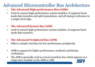
![Chapter2_fault tolerance [Compatibility Mode].pdf](https://cdn.slidesharecdn.com/ss_thumbnails/chapter2faulttolerancecompatibilitymode-241007004857-8eb7d95f-thumbnail.jpg?width=640&height=640&fit=bounds)