SlideShare a Scribd company logo
1 of 45
OPAMP
• Operational Amplifiers, or Op-amps as they are
more commonly called, are one of the basic
building blocks of Analogue Electronic Circuits
• An Operational Amplifier, or op-amp for short, is
fundamentally a voltage amplifying device
designed to be used with external feedback
components such as resistors and capacitors
between its output and input terminals.
Cont…
• These feedback components determine the
resulting function or “operation” of the
amplifier and by virtue of the different
feedback configurations whether resistive,
capacitive or both, the amplifier can perform a
variety of different operations, giving rise to
its name of “Operational Amplifier”.
Cont…
• An Operational Amplifier is basically a three-
terminal device which consists of two high
impedance inputs. One of the inputs is called
the Inverting Input, marked with a negative or
“minus” sign, ( – ). The other input is called
the Non-inverting Input, marked with a
positive or “plus” sign ( + ).
Symbol of OPAMP
Four different classifications of operational
amplifier gain.
• Voltage – Voltage “in” and Voltage “out”
• Current – Current “in” and Current “out”
• Transconductance – Voltage “in” and Current
“out”
• Transresistance – Current “in” and Voltage
“out”
PIN DIAGRAM OF OPMP
Equivalent Circuit of an Ideal
Operational Amplifier
• Vo = AVdiff = A (V1−V2)
• Which indicates that the output voltage Vo is
a function of the difference between the input
voltages V1 and V2. For this reason op-amps
are difference amplifiers.
Non-Linear Region:
• An Op-amp operates in non-linear or saturation region when it is in
open loop or positive feedback configuration.
• When Vp>Vn by 1mA then opamp will be in postitive saturation
region Vo=Vsat=+Vs.
• When Vn>Vp by 1mA then opamp will be in negative saturation
region Vo=-Vsat=-Vsupply
Linear Region:
• An Op-amp operates in linear when it is in negative feedback
configuration.
• Current through inverting and non-inverting terminal is zero.
• inverting and non-inverting terminal voltages are equal.
• Vo<|Vs| or A(Vp-Vn)<|Vs|
• Vp-Vn<|Vs|/A
Vs is 10V, 12V,15V, A=1000000 to 1000000000
Op-amp Parameter and Idealised
Characteristic
• Open Loop Gain, (Avo)-the gain will be infinite
but typical real values range from about
20,000 to 200,000.
• Input impedance, (ZIN-infinite)-Input impedance
is the ratio of input voltage to input current
and is assumed to be infinite to prevent any
current flowing from the source supply into
the amplifiers input circuitry ( IIN = 0 ).
Real op-amps have input leakage currents from
a few pico-amps to a few milli-amps.
Op-amp Parameter and Idealised
Characteristic
• Output impedance, (ZOUT-Zero)-The output
impedance of the ideal operational amplifier
is assumed to be zero acting as a perfect
internal voltage source with no internal
resistance so that it can supply as much
current as necessary to the load.
• Real op-amps have output impedances in the
100-20kΩ range.
Op-amp Parameter and Idealised
Characteristic
• Infinite – An ideal operational amplifier has an
infinite frequency response and can amplify
any frequency signal from DC to the highest
AC frequencies so it is therefore assumed to
have an infinite bandwidth.
• With real op-amps, the bandwidth is limited
by the Gain-Bandwidth product (GB), which is
equal to the frequency where the amplifiers
gain becomes unity.
Op-amp Parameter and Idealised
Characteristic
• Offset Voltage, (VIO)
• Zero – The amplifiers output will be zero when
the voltage difference between the inverting
and the non-inverting inputs is zero, the same
or when both inputs are grounded.
• Real op-amps have some amount of output
offset voltage.
• However, real Operational Amplifiers such as
the commonly available uA741, for example
do not have infinite gain or bandwidth but
have a typical “Open Loop Gain” which is
defined as the amplifiers output amplification
without any external feedback signals
connected to it and for a typical operational
amplifier is about 100dB at DC (zero Hz).
Open-loop Frequency Response Curve
Gain Bandwidth Product
• GBP = Gain x Bandwidth = A x BW
• Voltage Gain(A)=Vout/Vin
• In decibel 20log(A)
• An operational amplifiers bandwidth is
inversely proportional to its gain,
( A 1/∞ BW ). Also, this -3dB corner frequency
point is generally known as the “half power
point”, as the output power of the amplifier is
at half its maximum value
OPAMP Internal Diagram
• A component-level diagram of the common
741 op-amp. Dotted lines outline:
• Current mirrors/current source (red)
• Differential amplifier (blue)
• Class A gain stage (magenta)
• Voltage level shifter (green);
• output stage (cyan)
• Like all op-amps, the circuit basically consists
of three stages:
• Differential amplifier with high input
impedance that generates a voltage signal, the
amplified voltage difference .
• Voltage amplifier (class A amplification) with a
high voltage gain to further amplify the
voltage.
• Output amplifier (class AB push-pull emitter
follower) with low output impedance and high
current driving capability.
Summary
• We can connect external resistors or
capacitors to the op-amp in a number of
different ways to form basic “building Block”
circuits such as, Inverting, Non-Inverting,
Voltage Follower, Summing, Differential,
Integrator and Differentiator type amplifiers.
Inverting OPAMP
Inverting amplifier
• High gain is of no real use to us as it makes the
amplifier both unstable and hard to control as the
smallest of input signals.
• Negative Feedback is the process of “feeding
back” a fraction of the output signal back to the
input, but to make the feedback negative.
• We must feed it back to the negative or “inverting
input” terminal of the op-amp using an
external Feedback Resistor called Rƒ.
• This feedback connection between the output
and the inverting input terminal forces the
differential input voltage towards zero.
• This negative feedback results in the inverting input
terminal having a different signal on it than the actual
input voltage as it will be the sum of the input voltage
plus the negative feedback voltage giving it the label or
term of a Summing Point.
• We must therefore separate the real input signal from
the inverting input by using an Input Resistor, RIN.
• Feedback circuit results in the voltage potential at the
inverting input being equal to that at the non-inverting
input producing a Virtual Earth summing point because
it will be at the same potential as the grounded
reference input.
• In other words, the op-amp becomes a “differential
amplifier”.
• Two very important rules to remember
about Inverting Amplifiers or any operational
amplifier for that matter and these are.
• No Current Flows into the Input Terminals
• The Differential Input Voltage is Zero as V1 =
V2 = 0 (Virtual Earth)
• Then, the Closed-Loop Voltage Gain of an
Inverting Amplifier is given as.
• And this can be transposed to give Vout as:
The negative sign in the equation indicates an inversion of the output
signal with respect to the input as it is 180o out of phase. This is due
to the feedback being negative in value.
Vout = Vin x Gain. This property can be very useful for converting a
smaller sensor signal to a much larger voltage.
• Another useful application of an inverting
amplifier is that of a “transresistance amplifier”
circuit.
• A Transresistance Amplifier also known as a
“transimpedance amplifier”, is basically a current-
to-voltage converter (Current “in” and Voltage
“out”).
• They can be used in low-power applications to
convert a very small current generated by a
photo-diode or photo-detecting device etc, into a
usable output voltage which is proportional to
the input current as shown.
Transresistance Amplifier Circuit
• The simple light-activated circuit above,
converts a current generated by the photo-
diode into a voltage.
• The feedback resistor Rƒ sets the operating
voltage point at the inverting input and
controls the amount of output.
• The output voltage is given as Vout = -(Is x Rƒ).
Therefore, the output voltage is proportional
to the amount of input current generated by
the photo-diode.
Example:1
• Find the closed loop gain of the following
inverting amplifier circuit.
Non-Inverting Amp
• Feedback control of the non-inverting
operational amplifier is achieved by applying a
small part of the output voltage signal back to
the inverting ( – ) input terminal via a Rƒ –
R2 voltage divider network, again producing
negative feedback.
• High input impedance, Rin approaching
infinity, as no current flows into the positive
input terminal, (ideal conditions) and a low
output impedance,
Equivalent Potential Divider Network
Non-Inverting as Voltage Follower
Voltage Follower
• In this non-inverting circuit configuration, the
input impedance Rin has increased to infinity and
the feedback impedance Rƒ reduced to zero.
• The output is connected directly back to the
negative inverting input so the feedback is 100%
and Vin is exactly equal to Vout giving it a fixed
gain of 1 or unity.
• As the input voltage Vin is applied to the non-
inverting input the gain of the amplifier is given
as:
Summing Op-amp
Example No1
Find the output voltage of the
following Summing Amplifier circuit.
Digital to Analogue Converter (DAC)
Summing Amplifier Audio Mixer

More Related Content

What's hot

UNIT-III-Testing of DC Machines.ppt
UNIT-III-Testing of DC Machines.pptUNIT-III-Testing of DC Machines.ppt
UNIT-III-Testing of DC Machines.pptSaligantiKumar
 
DETERMINATION OF VOLTAGE REGULATION METHOD OF SYNCHRONOUS MACHINE
DETERMINATION OF VOLTAGE REGULATION METHOD OF SYNCHRONOUS MACHINEDETERMINATION OF VOLTAGE REGULATION METHOD OF SYNCHRONOUS MACHINE
DETERMINATION OF VOLTAGE REGULATION METHOD OF SYNCHRONOUS MACHINEvishalgohel12195
 
INVERTERS PRESENTATION
INVERTERS PRESENTATIONINVERTERS PRESENTATION
INVERTERS PRESENTATIONRajesh V
 
Dot convention in coupled circuits
Dot convention in coupled circuitsDot convention in coupled circuits
Dot convention in coupled circuitsmrunalinithanaraj
 
Unit-I Characteristics of opamp
Unit-I Characteristics of opampUnit-I Characteristics of opamp
Unit-I Characteristics of opampDr.Raja R
 
Invering and non inverting amplifiers
Invering and non inverting amplifiersInvering and non inverting amplifiers
Invering and non inverting amplifiersMuhammad Mohsin
 
Power electronics Phase Controlled Rectifiers - SCR
Power electronics   Phase Controlled Rectifiers - SCRPower electronics   Phase Controlled Rectifiers - SCR
Power electronics Phase Controlled Rectifiers - SCRBurdwan University
 
2.Opamp parameters
2.Opamp parameters2.Opamp parameters
2.Opamp parametersINDIAN NAVY
 
SUMMING AMPLIFIER
SUMMING AMPLIFIERSUMMING AMPLIFIER
SUMMING AMPLIFIERAK138
 
Unit 3 phase controlled converters
Unit 3 phase controlled convertersUnit 3 phase controlled converters
Unit 3 phase controlled convertersEr.Meraj Akhtar
 
3.bipolar junction transistor (bjt)
3.bipolar junction transistor (bjt)3.bipolar junction transistor (bjt)
3.bipolar junction transistor (bjt)firozamin
 
Operational amplifier
Operational amplifierOperational amplifier
Operational amplifierUnsa Shakir
 
Dual Slope ADC.pptx
Dual Slope ADC.pptxDual Slope ADC.pptx
Dual Slope ADC.pptxhepzijustin
 
Summing Amplifier
Summing AmplifierSumming Amplifier
Summing AmplifierDr.Raja R
 
Amplitude modulation & demodulation
Amplitude modulation & demodulation Amplitude modulation & demodulation
Amplitude modulation & demodulation Bikz013
 
operational amplifiers
operational amplifiersoperational amplifiers
operational amplifiersPatel Jay
 

What's hot (20)

UNIT-III-Testing of DC Machines.ppt
UNIT-III-Testing of DC Machines.pptUNIT-III-Testing of DC Machines.ppt
UNIT-III-Testing of DC Machines.ppt
 
DETERMINATION OF VOLTAGE REGULATION METHOD OF SYNCHRONOUS MACHINE
DETERMINATION OF VOLTAGE REGULATION METHOD OF SYNCHRONOUS MACHINEDETERMINATION OF VOLTAGE REGULATION METHOD OF SYNCHRONOUS MACHINE
DETERMINATION OF VOLTAGE REGULATION METHOD OF SYNCHRONOUS MACHINE
 
INVERTERS PRESENTATION
INVERTERS PRESENTATIONINVERTERS PRESENTATION
INVERTERS PRESENTATION
 
Dot convention in coupled circuits
Dot convention in coupled circuitsDot convention in coupled circuits
Dot convention in coupled circuits
 
Unit-I Characteristics of opamp
Unit-I Characteristics of opampUnit-I Characteristics of opamp
Unit-I Characteristics of opamp
 
OP-AMP.pptx
OP-AMP.pptxOP-AMP.pptx
OP-AMP.pptx
 
Invering and non inverting amplifiers
Invering and non inverting amplifiersInvering and non inverting amplifiers
Invering and non inverting amplifiers
 
Power electronics Phase Controlled Rectifiers - SCR
Power electronics   Phase Controlled Rectifiers - SCRPower electronics   Phase Controlled Rectifiers - SCR
Power electronics Phase Controlled Rectifiers - SCR
 
2.Opamp parameters
2.Opamp parameters2.Opamp parameters
2.Opamp parameters
 
SUMMING AMPLIFIER
SUMMING AMPLIFIERSUMMING AMPLIFIER
SUMMING AMPLIFIER
 
Op amps
Op ampsOp amps
Op amps
 
Unit 3 phase controlled converters
Unit 3 phase controlled convertersUnit 3 phase controlled converters
Unit 3 phase controlled converters
 
Op amp
Op ampOp amp
Op amp
 
3.bipolar junction transistor (bjt)
3.bipolar junction transistor (bjt)3.bipolar junction transistor (bjt)
3.bipolar junction transistor (bjt)
 
Operational amplifier
Operational amplifierOperational amplifier
Operational amplifier
 
Dual Slope ADC.pptx
Dual Slope ADC.pptxDual Slope ADC.pptx
Dual Slope ADC.pptx
 
Summing Amplifier
Summing AmplifierSumming Amplifier
Summing Amplifier
 
Amplitude modulation & demodulation
Amplitude modulation & demodulation Amplitude modulation & demodulation
Amplitude modulation & demodulation
 
operational amplifiers
operational amplifiersoperational amplifiers
operational amplifiers
 
Choppers
ChoppersChoppers
Choppers
 

Similar to Operating Amplifier

Similar to Operating Amplifier (20)

analog elecronic designLecture 2 (1).pptx
analog elecronic designLecture 2 (1).pptxanalog elecronic designLecture 2 (1).pptx
analog elecronic designLecture 2 (1).pptx
 
Op-Amp 1
Op-Amp 1Op-Amp 1
Op-Amp 1
 
Pin Connection of OP-AMP, Paramerters..pptx
Pin Connection of OP-AMP, Paramerters..pptxPin Connection of OP-AMP, Paramerters..pptx
Pin Connection of OP-AMP, Paramerters..pptx
 
Operation amplifier
Operation amplifierOperation amplifier
Operation amplifier
 
Electrica Transformer and filters high and lowpass.ppt
Electrica Transformer and filters high and lowpass.pptElectrica Transformer and filters high and lowpass.ppt
Electrica Transformer and filters high and lowpass.ppt
 
Operational amplifier
Operational amplifierOperational amplifier
Operational amplifier
 
Operationamplifier
OperationamplifierOperationamplifier
Operationamplifier
 
opamps
opampsopamps
opamps
 
op amp.pptx
op amp.pptxop amp.pptx
op amp.pptx
 
OP AMP Applications
OP AMP ApplicationsOP AMP Applications
OP AMP Applications
 
Sarah
SarahSarah
Sarah
 
UNIT-3 OPAMP.pptx
UNIT-3 OPAMP.pptxUNIT-3 OPAMP.pptx
UNIT-3 OPAMP.pptx
 
Operational amplifier
Operational amplifierOperational amplifier
Operational amplifier
 
Op amp basics
Op amp basicsOp amp basics
Op amp basics
 
operational amplifiers basic - introduction
operational amplifiers basic -  introductionoperational amplifiers basic -  introduction
operational amplifiers basic - introduction
 
Op amp
Op ampOp amp
Op amp
 
Electrical signal processing and transmission
Electrical signal processing and transmissionElectrical signal processing and transmission
Electrical signal processing and transmission
 
Op amp
Op amp Op amp
Op amp
 
B sc ii sem unit 1
B sc ii sem unit 1B sc ii sem unit 1
B sc ii sem unit 1
 
Arvi
ArviArvi
Arvi
 

Recently uploaded

Introduction-To-Agricultural-Surveillance-Rover.pptx
Introduction-To-Agricultural-Surveillance-Rover.pptxIntroduction-To-Agricultural-Surveillance-Rover.pptx
Introduction-To-Agricultural-Surveillance-Rover.pptxk795866
 
Call Us ≽ 8377877756 ≼ Call Girls In Shastri Nagar (Delhi)
Call Us ≽ 8377877756 ≼ Call Girls In Shastri Nagar (Delhi)Call Us ≽ 8377877756 ≼ Call Girls In Shastri Nagar (Delhi)
Call Us ≽ 8377877756 ≼ Call Girls In Shastri Nagar (Delhi)dollysharma2066
 
GDSC ASEB Gen AI study jams presentation
GDSC ASEB Gen AI study jams presentationGDSC ASEB Gen AI study jams presentation
GDSC ASEB Gen AI study jams presentationGDSCAESB
 
INFLUENCE OF NANOSILICA ON THE PROPERTIES OF CONCRETE
INFLUENCE OF NANOSILICA ON THE PROPERTIES OF CONCRETEINFLUENCE OF NANOSILICA ON THE PROPERTIES OF CONCRETE
INFLUENCE OF NANOSILICA ON THE PROPERTIES OF CONCRETEroselinkalist12
 
Application of Residue Theorem to evaluate real integrations.pptx
Application of Residue Theorem to evaluate real integrations.pptxApplication of Residue Theorem to evaluate real integrations.pptx
Application of Residue Theorem to evaluate real integrations.pptx959SahilShah
 
Current Transformer Drawing and GTP for MSETCL
Current Transformer Drawing and GTP for MSETCLCurrent Transformer Drawing and GTP for MSETCL
Current Transformer Drawing and GTP for MSETCLDeelipZope
 
CCS355 Neural Network & Deep Learning Unit II Notes with Question bank .pdf
CCS355 Neural Network & Deep Learning Unit II Notes with Question bank .pdfCCS355 Neural Network & Deep Learning Unit II Notes with Question bank .pdf
CCS355 Neural Network & Deep Learning Unit II Notes with Question bank .pdfAsst.prof M.Gokilavani
 
OSVC_Meta-Data based Simulation Automation to overcome Verification Challenge...
OSVC_Meta-Data based Simulation Automation to overcome Verification Challenge...OSVC_Meta-Data based Simulation Automation to overcome Verification Challenge...
OSVC_Meta-Data based Simulation Automation to overcome Verification Challenge...Soham Mondal
 
main PPT.pptx of girls hostel security using rfid
main PPT.pptx of girls hostel security using rfidmain PPT.pptx of girls hostel security using rfid
main PPT.pptx of girls hostel security using rfidNikhilNagaraju
 
Microscopic Analysis of Ceramic Materials.pptx
Microscopic Analysis of Ceramic Materials.pptxMicroscopic Analysis of Ceramic Materials.pptx
Microscopic Analysis of Ceramic Materials.pptxpurnimasatapathy1234
 
Biology for Computer Engineers Course Handout.pptx
Biology for Computer Engineers Course Handout.pptxBiology for Computer Engineers Course Handout.pptx
Biology for Computer Engineers Course Handout.pptxDeepakSakkari2
 
Sachpazis Costas: Geotechnical Engineering: A student's Perspective Introduction
Sachpazis Costas: Geotechnical Engineering: A student's Perspective IntroductionSachpazis Costas: Geotechnical Engineering: A student's Perspective Introduction
Sachpazis Costas: Geotechnical Engineering: A student's Perspective IntroductionDr.Costas Sachpazis
 
Software and Systems Engineering Standards: Verification and Validation of Sy...
Software and Systems Engineering Standards: Verification and Validation of Sy...Software and Systems Engineering Standards: Verification and Validation of Sy...
Software and Systems Engineering Standards: Verification and Validation of Sy...VICTOR MAESTRE RAMIREZ
 
Decoding Kotlin - Your guide to solving the mysterious in Kotlin.pptx
Decoding Kotlin - Your guide to solving the mysterious in Kotlin.pptxDecoding Kotlin - Your guide to solving the mysterious in Kotlin.pptx
Decoding Kotlin - Your guide to solving the mysterious in Kotlin.pptxJoão Esperancinha
 
VIP Call Girls Service Hitech City Hyderabad Call +91-8250192130
VIP Call Girls Service Hitech City Hyderabad Call +91-8250192130VIP Call Girls Service Hitech City Hyderabad Call +91-8250192130
VIP Call Girls Service Hitech City Hyderabad Call +91-8250192130Suhani Kapoor
 
Study on Air-Water & Water-Water Heat Exchange in a Finned Tube Exchanger
Study on Air-Water & Water-Water Heat Exchange in a Finned Tube ExchangerStudy on Air-Water & Water-Water Heat Exchange in a Finned Tube Exchanger
Study on Air-Water & Water-Water Heat Exchange in a Finned Tube ExchangerAnamika Sarkar
 

Recently uploaded (20)

Introduction-To-Agricultural-Surveillance-Rover.pptx
Introduction-To-Agricultural-Surveillance-Rover.pptxIntroduction-To-Agricultural-Surveillance-Rover.pptx
Introduction-To-Agricultural-Surveillance-Rover.pptx
 
Call Us ≽ 8377877756 ≼ Call Girls In Shastri Nagar (Delhi)
Call Us ≽ 8377877756 ≼ Call Girls In Shastri Nagar (Delhi)Call Us ≽ 8377877756 ≼ Call Girls In Shastri Nagar (Delhi)
Call Us ≽ 8377877756 ≼ Call Girls In Shastri Nagar (Delhi)
 
Design and analysis of solar grass cutter.pdf
Design and analysis of solar grass cutter.pdfDesign and analysis of solar grass cutter.pdf
Design and analysis of solar grass cutter.pdf
 
GDSC ASEB Gen AI study jams presentation
GDSC ASEB Gen AI study jams presentationGDSC ASEB Gen AI study jams presentation
GDSC ASEB Gen AI study jams presentation
 
INFLUENCE OF NANOSILICA ON THE PROPERTIES OF CONCRETE
INFLUENCE OF NANOSILICA ON THE PROPERTIES OF CONCRETEINFLUENCE OF NANOSILICA ON THE PROPERTIES OF CONCRETE
INFLUENCE OF NANOSILICA ON THE PROPERTIES OF CONCRETE
 
Application of Residue Theorem to evaluate real integrations.pptx
Application of Residue Theorem to evaluate real integrations.pptxApplication of Residue Theorem to evaluate real integrations.pptx
Application of Residue Theorem to evaluate real integrations.pptx
 
★ CALL US 9953330565 ( HOT Young Call Girls In Badarpur delhi NCR
★ CALL US 9953330565 ( HOT Young Call Girls In Badarpur delhi NCR★ CALL US 9953330565 ( HOT Young Call Girls In Badarpur delhi NCR
★ CALL US 9953330565 ( HOT Young Call Girls In Badarpur delhi NCR
 
Current Transformer Drawing and GTP for MSETCL
Current Transformer Drawing and GTP for MSETCLCurrent Transformer Drawing and GTP for MSETCL
Current Transformer Drawing and GTP for MSETCL
 
CCS355 Neural Network & Deep Learning Unit II Notes with Question bank .pdf
CCS355 Neural Network & Deep Learning Unit II Notes with Question bank .pdfCCS355 Neural Network & Deep Learning Unit II Notes with Question bank .pdf
CCS355 Neural Network & Deep Learning Unit II Notes with Question bank .pdf
 
Exploring_Network_Security_with_JA3_by_Rakesh Seal.pptx
Exploring_Network_Security_with_JA3_by_Rakesh Seal.pptxExploring_Network_Security_with_JA3_by_Rakesh Seal.pptx
Exploring_Network_Security_with_JA3_by_Rakesh Seal.pptx
 
OSVC_Meta-Data based Simulation Automation to overcome Verification Challenge...
OSVC_Meta-Data based Simulation Automation to overcome Verification Challenge...OSVC_Meta-Data based Simulation Automation to overcome Verification Challenge...
OSVC_Meta-Data based Simulation Automation to overcome Verification Challenge...
 
main PPT.pptx of girls hostel security using rfid
main PPT.pptx of girls hostel security using rfidmain PPT.pptx of girls hostel security using rfid
main PPT.pptx of girls hostel security using rfid
 
🔝9953056974🔝!!-YOUNG call girls in Rajendra Nagar Escort rvice Shot 2000 nigh...
🔝9953056974🔝!!-YOUNG call girls in Rajendra Nagar Escort rvice Shot 2000 nigh...🔝9953056974🔝!!-YOUNG call girls in Rajendra Nagar Escort rvice Shot 2000 nigh...
🔝9953056974🔝!!-YOUNG call girls in Rajendra Nagar Escort rvice Shot 2000 nigh...
 
Microscopic Analysis of Ceramic Materials.pptx
Microscopic Analysis of Ceramic Materials.pptxMicroscopic Analysis of Ceramic Materials.pptx
Microscopic Analysis of Ceramic Materials.pptx
 
Biology for Computer Engineers Course Handout.pptx
Biology for Computer Engineers Course Handout.pptxBiology for Computer Engineers Course Handout.pptx
Biology for Computer Engineers Course Handout.pptx
 
Sachpazis Costas: Geotechnical Engineering: A student's Perspective Introduction
Sachpazis Costas: Geotechnical Engineering: A student's Perspective IntroductionSachpazis Costas: Geotechnical Engineering: A student's Perspective Introduction
Sachpazis Costas: Geotechnical Engineering: A student's Perspective Introduction
 
Software and Systems Engineering Standards: Verification and Validation of Sy...
Software and Systems Engineering Standards: Verification and Validation of Sy...Software and Systems Engineering Standards: Verification and Validation of Sy...
Software and Systems Engineering Standards: Verification and Validation of Sy...
 
Decoding Kotlin - Your guide to solving the mysterious in Kotlin.pptx
Decoding Kotlin - Your guide to solving the mysterious in Kotlin.pptxDecoding Kotlin - Your guide to solving the mysterious in Kotlin.pptx
Decoding Kotlin - Your guide to solving the mysterious in Kotlin.pptx
 
VIP Call Girls Service Hitech City Hyderabad Call +91-8250192130
VIP Call Girls Service Hitech City Hyderabad Call +91-8250192130VIP Call Girls Service Hitech City Hyderabad Call +91-8250192130
VIP Call Girls Service Hitech City Hyderabad Call +91-8250192130
 
Study on Air-Water & Water-Water Heat Exchange in a Finned Tube Exchanger
Study on Air-Water & Water-Water Heat Exchange in a Finned Tube ExchangerStudy on Air-Water & Water-Water Heat Exchange in a Finned Tube Exchanger
Study on Air-Water & Water-Water Heat Exchange in a Finned Tube Exchanger
 

Operating Amplifier

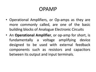
  • 1. OPAMP • Operational Amplifiers, or Op-amps as they are more commonly called, are one of the basic building blocks of Analogue Electronic Circuits • An Operational Amplifier, or op-amp for short, is fundamentally a voltage amplifying device designed to be used with external feedback components such as resistors and capacitors between its output and input terminals.
  • 2. Cont… • These feedback components determine the resulting function or “operation” of the amplifier and by virtue of the different feedback configurations whether resistive, capacitive or both, the amplifier can perform a variety of different operations, giving rise to its name of “Operational Amplifier”.
  • 3. Cont… • An Operational Amplifier is basically a three- terminal device which consists of two high impedance inputs. One of the inputs is called the Inverting Input, marked with a negative or “minus” sign, ( – ). The other input is called the Non-inverting Input, marked with a positive or “plus” sign ( + ).
  • 5. Four different classifications of operational amplifier gain. • Voltage – Voltage “in” and Voltage “out” • Current – Current “in” and Current “out” • Transconductance – Voltage “in” and Current “out” • Transresistance – Current “in” and Voltage “out”
  • 7. Equivalent Circuit of an Ideal Operational Amplifier
  • 8. • Vo = AVdiff = A (V1−V2) • Which indicates that the output voltage Vo is a function of the difference between the input voltages V1 and V2. For this reason op-amps are difference amplifiers.
  • 9.
  • 10. Non-Linear Region: • An Op-amp operates in non-linear or saturation region when it is in open loop or positive feedback configuration. • When Vp>Vn by 1mA then opamp will be in postitive saturation region Vo=Vsat=+Vs. • When Vn>Vp by 1mA then opamp will be in negative saturation region Vo=-Vsat=-Vsupply Linear Region: • An Op-amp operates in linear when it is in negative feedback configuration. • Current through inverting and non-inverting terminal is zero. • inverting and non-inverting terminal voltages are equal. • Vo<|Vs| or A(Vp-Vn)<|Vs| • Vp-Vn<|Vs|/A Vs is 10V, 12V,15V, A=1000000 to 1000000000
  • 11. Op-amp Parameter and Idealised Characteristic • Open Loop Gain, (Avo)-the gain will be infinite but typical real values range from about 20,000 to 200,000. • Input impedance, (ZIN-infinite)-Input impedance is the ratio of input voltage to input current and is assumed to be infinite to prevent any current flowing from the source supply into the amplifiers input circuitry ( IIN = 0 ). Real op-amps have input leakage currents from a few pico-amps to a few milli-amps.
  • 12. Op-amp Parameter and Idealised Characteristic • Output impedance, (ZOUT-Zero)-The output impedance of the ideal operational amplifier is assumed to be zero acting as a perfect internal voltage source with no internal resistance so that it can supply as much current as necessary to the load. • Real op-amps have output impedances in the 100-20kΩ range.
  • 13. Op-amp Parameter and Idealised Characteristic • Infinite – An ideal operational amplifier has an infinite frequency response and can amplify any frequency signal from DC to the highest AC frequencies so it is therefore assumed to have an infinite bandwidth. • With real op-amps, the bandwidth is limited by the Gain-Bandwidth product (GB), which is equal to the frequency where the amplifiers gain becomes unity.
  • 14. Op-amp Parameter and Idealised Characteristic • Offset Voltage, (VIO) • Zero – The amplifiers output will be zero when the voltage difference between the inverting and the non-inverting inputs is zero, the same or when both inputs are grounded. • Real op-amps have some amount of output offset voltage.
  • 15. • However, real Operational Amplifiers such as the commonly available uA741, for example do not have infinite gain or bandwidth but have a typical “Open Loop Gain” which is defined as the amplifiers output amplification without any external feedback signals connected to it and for a typical operational amplifier is about 100dB at DC (zero Hz).
  • 17. Gain Bandwidth Product • GBP = Gain x Bandwidth = A x BW • Voltage Gain(A)=Vout/Vin • In decibel 20log(A) • An operational amplifiers bandwidth is inversely proportional to its gain, ( A 1/∞ BW ). Also, this -3dB corner frequency point is generally known as the “half power point”, as the output power of the amplifier is at half its maximum value
  • 19. • A component-level diagram of the common 741 op-amp. Dotted lines outline: • Current mirrors/current source (red) • Differential amplifier (blue) • Class A gain stage (magenta) • Voltage level shifter (green); • output stage (cyan)
  • 20. • Like all op-amps, the circuit basically consists of three stages: • Differential amplifier with high input impedance that generates a voltage signal, the amplified voltage difference . • Voltage amplifier (class A amplification) with a high voltage gain to further amplify the voltage. • Output amplifier (class AB push-pull emitter follower) with low output impedance and high current driving capability.
  • 21. Summary • We can connect external resistors or capacitors to the op-amp in a number of different ways to form basic “building Block” circuits such as, Inverting, Non-Inverting, Voltage Follower, Summing, Differential, Integrator and Differentiator type amplifiers.
  • 23. Inverting amplifier • High gain is of no real use to us as it makes the amplifier both unstable and hard to control as the smallest of input signals. • Negative Feedback is the process of “feeding back” a fraction of the output signal back to the input, but to make the feedback negative. • We must feed it back to the negative or “inverting input” terminal of the op-amp using an external Feedback Resistor called Rƒ. • This feedback connection between the output and the inverting input terminal forces the differential input voltage towards zero.
  • 24. • This negative feedback results in the inverting input terminal having a different signal on it than the actual input voltage as it will be the sum of the input voltage plus the negative feedback voltage giving it the label or term of a Summing Point. • We must therefore separate the real input signal from the inverting input by using an Input Resistor, RIN. • Feedback circuit results in the voltage potential at the inverting input being equal to that at the non-inverting input producing a Virtual Earth summing point because it will be at the same potential as the grounded reference input. • In other words, the op-amp becomes a “differential amplifier”.
  • 25. • Two very important rules to remember about Inverting Amplifiers or any operational amplifier for that matter and these are. • No Current Flows into the Input Terminals • The Differential Input Voltage is Zero as V1 = V2 = 0 (Virtual Earth)
  • 26.
  • 27. • Then, the Closed-Loop Voltage Gain of an Inverting Amplifier is given as. • And this can be transposed to give Vout as:
  • 28. The negative sign in the equation indicates an inversion of the output signal with respect to the input as it is 180o out of phase. This is due to the feedback being negative in value. Vout = Vin x Gain. This property can be very useful for converting a smaller sensor signal to a much larger voltage.
  • 29. • Another useful application of an inverting amplifier is that of a “transresistance amplifier” circuit. • A Transresistance Amplifier also known as a “transimpedance amplifier”, is basically a current- to-voltage converter (Current “in” and Voltage “out”). • They can be used in low-power applications to convert a very small current generated by a photo-diode or photo-detecting device etc, into a usable output voltage which is proportional to the input current as shown.
  • 31. Transresistance Amplifier Circuit • The simple light-activated circuit above, converts a current generated by the photo- diode into a voltage. • The feedback resistor Rƒ sets the operating voltage point at the inverting input and controls the amount of output. • The output voltage is given as Vout = -(Is x Rƒ). Therefore, the output voltage is proportional to the amount of input current generated by the photo-diode.
  • 32. Example:1 • Find the closed loop gain of the following inverting amplifier circuit.
  • 34. • Feedback control of the non-inverting operational amplifier is achieved by applying a small part of the output voltage signal back to the inverting ( – ) input terminal via a Rƒ – R2 voltage divider network, again producing negative feedback. • High input impedance, Rin approaching infinity, as no current flows into the positive input terminal, (ideal conditions) and a low output impedance,
  • 36.
  • 37.
  • 39. Voltage Follower • In this non-inverting circuit configuration, the input impedance Rin has increased to infinity and the feedback impedance Rƒ reduced to zero. • The output is connected directly back to the negative inverting input so the feedback is 100% and Vin is exactly equal to Vout giving it a fixed gain of 1 or unity. • As the input voltage Vin is applied to the non- inverting input the gain of the amplifier is given as:
  • 40.
  • 42.
  • 43. Example No1 Find the output voltage of the following Summing Amplifier circuit.
  • 44. Digital to Analogue Converter (DAC)