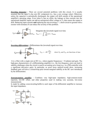
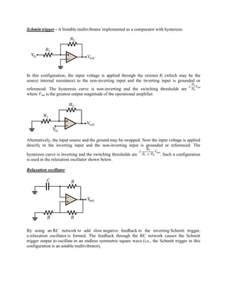
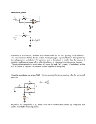
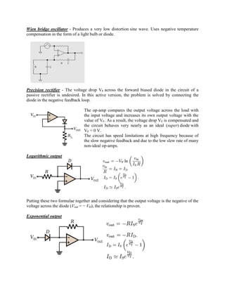
NATIONAL COLLEGE OF SCIENCE AND TECHNOLOGY
                     Amafel Building, Aguinaldo Highway Dasmariñas City, Cavite


                                ASSIGNMENT # 1
                            OPERATIONAL AMPLIFIER


Agdon, Berverlyn B.                                                July 26, 2011
Electronics 3/BSECE 41A1                                           Score:


                                 Engr. Grace Ramones
                                       Instructor
OPERATIONAL AMPLIFIERS
         It is an amplifier which is designed to be used with other circuit components to perform
either computing functions (addition, subtraction) or some type of transfer operation, such as
filtering. Operational amplifiers are usually high-gain amplifiers with the amount of gain
determined by feedback.
          Schematic symbols of an op amp


Characterstics of Op-Amp
         1. Very high gain
         2. Very high input impedance
         3. Very low output impedance
Since no single amplifier stage can provide all these characteristics well enough to be considered
an operational amplifier, various amplifier stages are connected together. The total circuit made
up of these individual stages is called an operational amplifier. This circuit (the operational
amplifier) can be made up of individual components (transistors, resistors, capacitors, etc.), but
the most common form of the operational amplifier is an integrated circuit. The integrated circuit
(chip) will contain the various stages of the operational amplifier and can be treated and used as
if it were a single stage.

Block diagram of Op-Amp
Types Of Op-Amps

Comparator- Compares two voltages and switches its output to indicate which voltage is larger.


Inverting amplifier - uses negative feedback to invert and amplify a voltage. The Rin,Rf resistor
network allows some of the output signal to be returned to the input. Since the output is 180° out
of phase, this amount is effectively subtracted from the input, thereby reducing the input into the
operational amplifier. This reduces the overall gain of the amplifier and is dubbed negative
feedback.


                                       Zin = Rin (because V − is a virtual ground)


Theory of operation: An Ideal Operational Amplifier has 2 characteristics that imply the
operation of the inverting amplifier: Infinite input impedance, and infinite differential gain.
Infinite input impedance implies there is no current in either of the input pins because current
cannot flow through an infinite impedance. Infinite differential gain implies that both the (+) and
(-) input pins are at the same voltage because the output is equal to infinity times (V+ - V-). As
the output approaches any arbitrary finite voltage, then the term (V+ - V-) approaches 0, thus the
two input pins are at the same voltage for any finite output.

Non-inverting amplifier - amplifies a voltage (multiplies by a constant greater than 1)


Although this circuit has a large input impedance, it suffers from error of input bias current.
The non-inverting ( + ) and inverting ( − ) inputs draw small leakage currents into the operational
amplifier. These input currents generate voltages that act like unmodeled input offsets. These
unmodeled effects can lead to noise on the output (e.g., offsets or drift). Assuming that the two
leaking currents are matched, their effect can be mitigated by ensuring the DC impedance
looking out of each input is the same. The voltage produced by each bias current is equal to the
product of the bias current with the equivalent DC impedance looking out of each input. Making
those impedances equal makes the offset voltage at each input equal, and so the non-zero bias
currents will have no impact on the difference between the two inputs.
Differential amplifier - the difference of two voltages each multiplied by some constant
(determined by the resistors).


Voltage follower (Unity Buffer Amplifier) - Used as a buffer amplifier to eliminate loading
effects (e.g., connecting a device with a high source impedance to a device with a low input
impedance).


Due to the strong (i.e., unity gain) feedback and certain non-ideal characteristics of real
operational amplifiers, this feedback system is prone to have poor stability margins.
Consequently, the system may be unstable when connected to sufficiently capacitive loads. In
these cases, alag compensation network (e.g., connecting the load to the voltage follower through
a resistor) can be used to restore stability. The manufacturer data sheet for the operational
amplifier may provide guidance for the selection of components in external compensation
networks. Alternatively, another operational amplifier can be chosen that has more appropriate
internal compensation.


Summing amplifier


                                    When                     , and Rf independent


                                    When

                                    Zn = Rn
Inverting integrator - There are several potential problems with this circuit. It is usually
assumed that the input Vin has zero DC component (i.e., has a zero average value). Otherwise,
unless the capacitor is periodically discharged, the output will drift outside of the operational
amplifier's operating range. Even when Vin has no offset, the leakage or bias currents into the
operational amplifier inputs can add an unexpected offset voltage to Vin that causes the output to
drift. Balancing input currents and replacing the non-inverting ( + ) short-circuit to ground with a
resistor with resistance R can reduce the severity of this problem.


                                   Integrates the (inverted) signal over time


Inverting differentiator - Differentiates the (inverted) signal over time.


 It is a filter with a single zero at DC (i.e., where angular frequencyω = 0 radians) and gain. The
high-pass characteristics of a differentiating amplifier (i.e., the low-frequency zero) can lead to
stability challenges when the circuit is used in an analog servo loop (e.g., in a PID controller with
a significant derivative gain). In particular, as aroot locus analysis would show, increasing
feedback gain will drive a closed-loop pole toward marginal stability at the DC zero introduced
by the differentiator.


Instrumentation amplifier - Combines very high input impedance, high common-mode
rejection, low DC offset, and other properties used in making very accurate, low-noise
measurements
Is made by adding a non-inverting buffer to each input of the differential amplifier to increase
the input impedance.
Schmitt trigger - A bistable multivibrator implemented as a comparator with hysteresis.


In this configuration, the input voltage is applied through the resistor R1 (which may be the
source internal resistance) to the non-inverting input and the inverting input is grounded or
referenced. The hysteresis curve is non-inverting and the switching thresholds are
where Vsat is the greatest output magnitude of the operational amplifier.


Alternatively, the input source and the ground may be swapped. Now the input voltage is applied
directly to the inverting input and the non-inverting input is grounded or referenced. The

hysteresis curve is inverting and the switching thresholds are             . Such a configuration
is used in the relaxation oscillator shown below.

Relaxation oscillator


By using an RC network to add slow negative feedback to the inverting Schmitt trigger,
a relaxation oscillator is formed. The feedback through the RC network causes the Schmitt
trigger output to oscillate in an endless symmetric square wave (i.e., the Schmitt trigger in this
configuration is an astable multivibrator).
Inductance gyrator


Simulates an inductor (i.e., provides inductance without the use of a possibly costly inductor).
The circuit exploits the fact that the current flowing through a capacitor behaves through time as
the voltage across an inductor. The capacitor used in this circuit is smaller than the inductor it
simulates and its capacitance is less subject to changes in value due to environmental changes.
This circuit is unsuitable for applications relying on the back EMF property of an inductor as this
will be limited in a gyrator circuit to the voltage supplies of the op-amp.


Negative impedance converter (NIC) - Creates a resistor having a negative value for any signal
generator


In general, the components R1, R2, and R3 need not be resistors; they can be any component that
can be described with an impedance.
Wien bridge oscillator - Produces a very low distortion sine wave. Uses negative temperature
compensation in the form of a light bulb or diode.


Precision rectifier - The voltage drop VF across the forward biased diode in the circuit of a
passive rectifier is undesired. In this active version, the problem is solved by connecting the
diode in the negative feedback loop.

                                The op-amp compares the output voltage across the load with
                                the input voltage and increases its own output voltage with the
                                value of VF. As a result, the voltage drop VF is compensated and
                                the circuit behaves very nearly as an ideal (super) diode with
                                VF = 0 V.
                                The circuit has speed limitations at high frequency because of
                                the slow negative feedback and due to the low slew rate of many
                                non-ideal op-amps.

Logarithmic output


Putting these two formulae together and considering that the output voltage is the negative of the
voltage across the diode (Vout = − VD), the relationship is proven.

Exponential output

Agdon

  • 1.
    NATIONAL COLLEGE OFSCIENCE AND TECHNOLOGY Amafel Building, Aguinaldo Highway Dasmariñas City, Cavite ASSIGNMENT # 1 OPERATIONAL AMPLIFIER Agdon, Berverlyn B. July 26, 2011 Electronics 3/BSECE 41A1 Score: Engr. Grace Ramones Instructor
  • 2.
    OPERATIONAL AMPLIFIERS It is an amplifier which is designed to be used with other circuit components to perform either computing functions (addition, subtraction) or some type of transfer operation, such as filtering. Operational amplifiers are usually high-gain amplifiers with the amount of gain determined by feedback. Schematic symbols of an op amp Characterstics of Op-Amp 1. Very high gain 2. Very high input impedance 3. Very low output impedance Since no single amplifier stage can provide all these characteristics well enough to be considered an operational amplifier, various amplifier stages are connected together. The total circuit made up of these individual stages is called an operational amplifier. This circuit (the operational amplifier) can be made up of individual components (transistors, resistors, capacitors, etc.), but the most common form of the operational amplifier is an integrated circuit. The integrated circuit (chip) will contain the various stages of the operational amplifier and can be treated and used as if it were a single stage. Block diagram of Op-Amp
  • 3.
    Types Of Op-Amps Comparator-Compares two voltages and switches its output to indicate which voltage is larger. Inverting amplifier - uses negative feedback to invert and amplify a voltage. The Rin,Rf resistor network allows some of the output signal to be returned to the input. Since the output is 180° out of phase, this amount is effectively subtracted from the input, thereby reducing the input into the operational amplifier. This reduces the overall gain of the amplifier and is dubbed negative feedback. Zin = Rin (because V − is a virtual ground) Theory of operation: An Ideal Operational Amplifier has 2 characteristics that imply the operation of the inverting amplifier: Infinite input impedance, and infinite differential gain. Infinite input impedance implies there is no current in either of the input pins because current cannot flow through an infinite impedance. Infinite differential gain implies that both the (+) and (-) input pins are at the same voltage because the output is equal to infinity times (V+ - V-). As the output approaches any arbitrary finite voltage, then the term (V+ - V-) approaches 0, thus the two input pins are at the same voltage for any finite output. Non-inverting amplifier - amplifies a voltage (multiplies by a constant greater than 1) Although this circuit has a large input impedance, it suffers from error of input bias current. The non-inverting ( + ) and inverting ( − ) inputs draw small leakage currents into the operational amplifier. These input currents generate voltages that act like unmodeled input offsets. These unmodeled effects can lead to noise on the output (e.g., offsets or drift). Assuming that the two leaking currents are matched, their effect can be mitigated by ensuring the DC impedance looking out of each input is the same. The voltage produced by each bias current is equal to the product of the bias current with the equivalent DC impedance looking out of each input. Making those impedances equal makes the offset voltage at each input equal, and so the non-zero bias
  • 4.
    currents will haveno impact on the difference between the two inputs. Differential amplifier - the difference of two voltages each multiplied by some constant (determined by the resistors). Voltage follower (Unity Buffer Amplifier) - Used as a buffer amplifier to eliminate loading effects (e.g., connecting a device with a high source impedance to a device with a low input impedance). Due to the strong (i.e., unity gain) feedback and certain non-ideal characteristics of real operational amplifiers, this feedback system is prone to have poor stability margins. Consequently, the system may be unstable when connected to sufficiently capacitive loads. In these cases, alag compensation network (e.g., connecting the load to the voltage follower through a resistor) can be used to restore stability. The manufacturer data sheet for the operational amplifier may provide guidance for the selection of components in external compensation networks. Alternatively, another operational amplifier can be chosen that has more appropriate internal compensation. Summing amplifier When , and Rf independent When Zn = Rn
  • 5.
    Inverting integrator -There are several potential problems with this circuit. It is usually assumed that the input Vin has zero DC component (i.e., has a zero average value). Otherwise, unless the capacitor is periodically discharged, the output will drift outside of the operational amplifier's operating range. Even when Vin has no offset, the leakage or bias currents into the operational amplifier inputs can add an unexpected offset voltage to Vin that causes the output to drift. Balancing input currents and replacing the non-inverting ( + ) short-circuit to ground with a resistor with resistance R can reduce the severity of this problem. Integrates the (inverted) signal over time Inverting differentiator - Differentiates the (inverted) signal over time. It is a filter with a single zero at DC (i.e., where angular frequencyω = 0 radians) and gain. The high-pass characteristics of a differentiating amplifier (i.e., the low-frequency zero) can lead to stability challenges when the circuit is used in an analog servo loop (e.g., in a PID controller with a significant derivative gain). In particular, as aroot locus analysis would show, increasing feedback gain will drive a closed-loop pole toward marginal stability at the DC zero introduced by the differentiator. Instrumentation amplifier - Combines very high input impedance, high common-mode rejection, low DC offset, and other properties used in making very accurate, low-noise measurements Is made by adding a non-inverting buffer to each input of the differential amplifier to increase the input impedance.
  • 6.
    Schmitt trigger -A bistable multivibrator implemented as a comparator with hysteresis. In this configuration, the input voltage is applied through the resistor R1 (which may be the source internal resistance) to the non-inverting input and the inverting input is grounded or referenced. The hysteresis curve is non-inverting and the switching thresholds are where Vsat is the greatest output magnitude of the operational amplifier. Alternatively, the input source and the ground may be swapped. Now the input voltage is applied directly to the inverting input and the non-inverting input is grounded or referenced. The hysteresis curve is inverting and the switching thresholds are . Such a configuration is used in the relaxation oscillator shown below. Relaxation oscillator By using an RC network to add slow negative feedback to the inverting Schmitt trigger, a relaxation oscillator is formed. The feedback through the RC network causes the Schmitt trigger output to oscillate in an endless symmetric square wave (i.e., the Schmitt trigger in this configuration is an astable multivibrator).
  • 7.
    Inductance gyrator Simulates aninductor (i.e., provides inductance without the use of a possibly costly inductor). The circuit exploits the fact that the current flowing through a capacitor behaves through time as the voltage across an inductor. The capacitor used in this circuit is smaller than the inductor it simulates and its capacitance is less subject to changes in value due to environmental changes. This circuit is unsuitable for applications relying on the back EMF property of an inductor as this will be limited in a gyrator circuit to the voltage supplies of the op-amp. Negative impedance converter (NIC) - Creates a resistor having a negative value for any signal generator In general, the components R1, R2, and R3 need not be resistors; they can be any component that can be described with an impedance.
  • 8.
    Wien bridge oscillator- Produces a very low distortion sine wave. Uses negative temperature compensation in the form of a light bulb or diode. Precision rectifier - The voltage drop VF across the forward biased diode in the circuit of a passive rectifier is undesired. In this active version, the problem is solved by connecting the diode in the negative feedback loop. The op-amp compares the output voltage across the load with the input voltage and increases its own output voltage with the value of VF. As a result, the voltage drop VF is compensated and the circuit behaves very nearly as an ideal (super) diode with VF = 0 V. The circuit has speed limitations at high frequency because of the slow negative feedback and due to the low slew rate of many non-ideal op-amps. Logarithmic output Putting these two formulae together and considering that the output voltage is the negative of the voltage across the diode (Vout = − VD), the relationship is proven. Exponential output