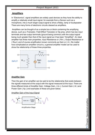
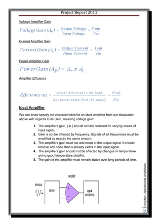
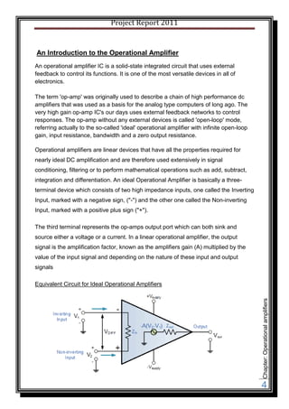
This presentation contains the basic information you need to know about operational amplifier.
I have tried to cover all the basic info. If anything is left out or you have any suggestions i will appreciate it.
This presentation contains the basic information you need to know about operational amplifier.
I have tried to cover all the basic info. If anything is left out or you have any suggestions i will appreciate it.
EST 130, Transistor Biasing and Amplification.CKSunith1
The attached narrated power point presentation explains the need for biasing in transistor amplifiers and the different biasing arrangements used in transistor circuits. The material will be useful for KTU first year B Tech students who prepare for the subject EST 130, Part B, Basic Electronics Engineering.
Negative amplifiers and its types Positive feedback and Negative feedbackimtiazalijoono
Negative amplifiers
What is Feedback?
Positive feedback
Negative feedback
Feedback Circuit
Principles of Negative Voltage Feedback In Amplifiers
Gain of Negative Voltage Feedback Amplifier
Advantages of Negative Voltage Feedback
Principles of Negative Current Feedback
Current Gain with Negative Current Feedback
Using Chebyshev filter design, there are two sub groups,
Type-I Chebyshev Filter
Type-II Chebyshev Filter
The major difference between butterworth and chebyshev filter is that the poles of butterworth filter lie on the circle while the poles of chebyshev filter lie on ellipse.
The performance obtainable from a single-stage amplifier is often insufficient for many applications, hence several stages may be combined forming a multistage amplifier. These stages are connected in cascade, i.e. output of the first stage is connected to form input of second stage, whose output becomes input of third stage, and so on.
thank u
Hansraj MEENA
Introduction
Band Pass Amplifiers
Series & Parallel Resonant Circuits & their Bandwidth
Analysis of Single Tuned Amplifiers
Analysis of Double Tuned Amplifiers
Primary & Secondary Tuned Amplifiers with BJT & FET
Merits and de-merits of Tuned Amplifiers
Letterbox Love: Why The Direct Mail Industry Is GrowingMarketscan
Snail mail is often used as a whipping boy when compared to email marketing. But ignore its strengths at your peril – because recent surveys show that we, the public, still love our letterboxes...
Photo resistor devices its working and applications.Soudip Sinha Roy
Here you will get every details about photo resistor device and its applications. How it makes in factory. And the important thing is The Light-Controlled Switch Using a Transistor.
Engineering design: A model of notification post boxalwzshalini
The main function of the “Notibox” is to notify the user when there is/are letter(s) inside the letter box. The notification is only given when the user open the house main door.
Presentation on Op-amp by Sourabh kumarSourabh Kumar
Visit Andro Root ( http:\\www.androroot.com ) for Tech. news and Smartphones.
Presentation on Op-amp(Operational Amplifier) by Sourabh kumar. B.tech Presentation,
Block diagram of a typical op-amp – characteristics of ideal and practical op-amp - parameters of opamp – inverting and non-inverting amplifier configurations - frequency response - circuit stability.
EDC Unit-4 Operational Amplifiers (Op-Amps) | RGPV De BunkersRGPV De Bunkers
Electronic Devices & Circuits - Operational Amplifiers (Op-Amps)
University Name: Rajiv Gandhi Proudyogiki Vishwavidyalaya, Bhopal
System: CBCS/CBGS
Program: Bachelor of Engineering in Computer Science
Semester: 3
Subject: Electronic Devices & Circuits
Description:
This comprehensive PDF study material explores Operational Amplifiers (Op-Amps) in Electronic Devices & Circuits for Semester 3 of the Bachelor of Engineering in Computer Science program at Rajiv Gandhi Proudyogiki Vishwavidyalaya, Bhopal.
Op-Amps are fundamental in analog circuits, known for their versatility and high gain. Topics covered include Op-Amp characteristics (high input impedance, low output impedance, etc.), slew rate, full power bandwidth, offset voltage, bias current, and practical applications like inverting/non-inverting amplifiers, differentiators, integrators, differential amplifiers, instrumentation amplifiers, and more.
This resource equips students to design and analyze electronic circuits, addressing real-world engineering challenges in communication systems, signal processing, instrumentation, etc.
Generating a custom Ruby SDK for your web service or Rails API using Smithyg2nightmarescribd
Have you ever wanted a Ruby client API to communicate with your web service? Smithy is a protocol-agnostic language for defining services and SDKs. Smithy Ruby is an implementation of Smithy that generates a Ruby SDK using a Smithy model. In this talk, we will explore Smithy and Smithy Ruby to learn how to generate custom feature-rich SDKs that can communicate with any web service, such as a Rails JSON API.
JMeter webinar - integration with InfluxDB and GrafanaRTTS
Watch this recorded webinar about real-time monitoring of application performance. See how to integrate Apache JMeter, the open-source leader in performance testing, with InfluxDB, the open-source time-series database, and Grafana, the open-source analytics and visualization application.
In this webinar, we will review the benefits of leveraging InfluxDB and Grafana when executing load tests and demonstrate how these tools are used to visualize performance metrics.
Length: 30 minutes
Session Overview
-------------------------------------------
During this webinar, we will cover the following topics while demonstrating the integrations of JMeter, InfluxDB and Grafana:
- What out-of-the-box solutions are available for real-time monitoring JMeter tests?
- What are the benefits of integrating InfluxDB and Grafana into the load testing stack?
- Which features are provided by Grafana?
- Demonstration of InfluxDB and Grafana using a practice web application
To view the webinar recording, go to:
https://www.rttsweb.com/jmeter-integration-webinar
GraphRAG is All You need? LLM & Knowledge GraphGuy Korland
Guy Korland, CEO and Co-founder of FalkorDB, will review two articles on the integration of language models with knowledge graphs.
1. Unifying Large Language Models and Knowledge Graphs: A Roadmap.
https://arxiv.org/abs/2306.08302
2. Microsoft Research's GraphRAG paper and a review paper on various uses of knowledge graphs:
https://www.microsoft.com/en-us/research/blog/graphrag-unlocking-llm-discovery-on-narrative-private-data/
Key Trends Shaping the Future of Infrastructure.pdfCheryl Hung
Keynote at DIGIT West Expo, Glasgow on 29 May 2024.
Cheryl Hung, ochery.com
Sr Director, Infrastructure Ecosystem, Arm.
The key trends across hardware, cloud and open-source; exploring how these areas are likely to mature and develop over the short and long-term, and then considering how organisations can position themselves to adapt and thrive.
LF Energy Webinar: Electrical Grid Modelling and Simulation Through PowSyBl -...DanBrown980551
Do you want to learn how to model and simulate an electrical network from scratch in under an hour?
Then welcome to this PowSyBl workshop, hosted by Rte, the French Transmission System Operator (TSO)!
During the webinar, you will discover the PowSyBl ecosystem as well as handle and study an electrical network through an interactive Python notebook.
PowSyBl is an open source project hosted by LF Energy, which offers a comprehensive set of features for electrical grid modelling and simulation. Among other advanced features, PowSyBl provides:
- A fully editable and extendable library for grid component modelling;
- Visualization tools to display your network;
- Grid simulation tools, such as power flows, security analyses (with or without remedial actions) and sensitivity analyses;
The framework is mostly written in Java, with a Python binding so that Python developers can access PowSyBl functionalities as well.
What you will learn during the webinar:
- For beginners: discover PowSyBl's functionalities through a quick general presentation and the notebook, without needing any expert coding skills;
- For advanced developers: master the skills to efficiently apply PowSyBl functionalities to your real-world scenarios.
Smart TV Buyer Insights Survey 2024 by 91mobiles.pdf91mobiles
91mobiles recently conducted a Smart TV Buyer Insights Survey in which we asked over 3,000 respondents about the TV they own, aspects they look at on a new TV, and their TV buying preferences.
Dev Dives: Train smarter, not harder – active learning and UiPath LLMs for do...UiPathCommunity
💥 Speed, accuracy, and scaling – discover the superpowers of GenAI in action with UiPath Document Understanding and Communications Mining™:
See how to accelerate model training and optimize model performance with active learning
Learn about the latest enhancements to out-of-the-box document processing – with little to no training required
Get an exclusive demo of the new family of UiPath LLMs – GenAI models specialized for processing different types of documents and messages
This is a hands-on session specifically designed for automation developers and AI enthusiasts seeking to enhance their knowledge in leveraging the latest intelligent document processing capabilities offered by UiPath.
Speakers:
👨🏫 Andras Palfi, Senior Product Manager, UiPath
👩🏫 Lenka Dulovicova, Product Program Manager, UiPath
Software Delivery At the Speed of AI: Inflectra Invests In AI-Powered QualityInflectra
In this insightful webinar, Inflectra explores how artificial intelligence (AI) is transforming software development and testing. Discover how AI-powered tools are revolutionizing every stage of the software development lifecycle (SDLC), from design and prototyping to testing, deployment, and monitoring.
Learn about:
• The Future of Testing: How AI is shifting testing towards verification, analysis, and higher-level skills, while reducing repetitive tasks.
• Test Automation: How AI-powered test case generation, optimization, and self-healing tests are making testing more efficient and effective.
• Visual Testing: Explore the emerging capabilities of AI in visual testing and how it's set to revolutionize UI verification.
• Inflectra's AI Solutions: See demonstrations of Inflectra's cutting-edge AI tools like the ChatGPT plugin and Azure Open AI platform, designed to streamline your testing process.
Whether you're a developer, tester, or QA professional, this webinar will give you valuable insights into how AI is shaping the future of software delivery.
State of ICS and IoT Cyber Threat Landscape Report 2024 previewPrayukth K V
The IoT and OT threat landscape report has been prepared by the Threat Research Team at Sectrio using data from Sectrio, cyber threat intelligence farming facilities spread across over 85 cities around the world. In addition, Sectrio also runs AI-based advanced threat and payload engagement facilities that serve as sinks to attract and engage sophisticated threat actors, and newer malware including new variants and latent threats that are at an earlier stage of development.
The latest edition of the OT/ICS and IoT security Threat Landscape Report 2024 also covers:
State of global ICS asset and network exposure
Sectoral targets and attacks as well as the cost of ransom
Global APT activity, AI usage, actor and tactic profiles, and implications
Rise in volumes of AI-powered cyberattacks
Major cyber events in 2024
Malware and malicious payload trends
Cyberattack types and targets
Vulnerability exploit attempts on CVEs
Attacks on counties – USA
Expansion of bot farms – how, where, and why
In-depth analysis of the cyber threat landscape across North America, South America, Europe, APAC, and the Middle East
Why are attacks on smart factories rising?
Cyber risk predictions
Axis of attacks – Europe
Systemic attacks in the Middle East
Download the full report from here:
https://sectrio.com/resources/ot-threat-landscape-reports/sectrio-releases-ot-ics-and-iot-security-threat-landscape-report-2024/
State of ICS and IoT Cyber Threat Landscape Report 2024 preview
Project electronic
1. Project Report 2011
Table of Contents
i) Amplifiers……….………………………………………………………………02
ii) Ideal amplifier……………………….………………………………………….03
iii) An introduction to the operational amplifier………………….……………...04
(1) Ideal
characteristics.……………………………………………………………..05
(2) Practical
characteristics………………………..…………………….………………06
iv) Limitations of the op-amp……………………………………..………………06
v) Applications of OP-AMPS……………………………………..……………...06
(1) As an
Integrator……………………………………………………………………07
(2) As a
Differentiator………………………………………………………………..10
(3) As an
Inverter………………………………………………………………………13
vi) As a Comparator…………………….…………………………………………17
vii) Overview of uA741 ……………………………………………………………18
viii)Given Task……………………………………………………………………...20
ix) Problems regarding Project and their Solutions……………………………20
x) Future Direction………………………………………………………………...23
xi) References……………………………………………………………………...24
Chapter: Operational amplifiers
1
2. Project Report 2011
Amplifiers
In "Electronics", signal amplifiers are widely used devices as they have the ability to
amplify a relatively small input signal, for example from a Sensor such as a
microphone, into a much larger output signal to drive a Relay, lamp or loudspeaker
There are many forms of electronic circuits classed as amplifiers.
Amplifiers can be thought of as a simple box or block containing the amplifying
device, such as a Transistor, Field Effect Transistor or Op-amp, which has two input
terminals and two output terminals (ground being common) with the output signal
being much greater than that of the input signal as it has been "Amplified”. An ideal
amplifier has three main properties, Input Resistance or ( Rin ), Output Resistance or
( Rout ) and of course amplification known commonly as Gain or ( A ). No matter
how complicated an amplifier circuit is, a general amplifier model can be used to
show the relationship of these three properties.
Amplifier Gain
Then the gain of an amplifier can be said to be the relationship that exists between
the signals measured at the output with the signal measured at the input. There are
three different kinds of Amplifier Gain, Voltage Gain, ( Av ), Current Gain ( Ai ) and
Power Gain ( Ap ) and examples of these are given below.
Amplifier Gain of the Input Signal
Chapter: Operational amplifiers
2
3. Project Report 2011
Voltage Amplifier Gain
Current Amplifier Gain
Power Amplifier Gain
Amplifier Efficiency
Ideal Amplifier
We can know specify the characteristics for an ideal amplifier from our discussion
above with regards to its Gain, meaning voltage gain:
1. The amplifiers gain, ( A ) should remain constant for varying values of
input signal.
2. Gain is not be affected by frequency. Signals of all frequencies must be
amplified by exactly the same amount.
3. The amplifiers gain must not add noise to the output signal. It should
remove any noise that is already exists in the input signal.
4. The amplifiers gain should not be affected by changes in temperature
giving good temperature stability.
5. The gain of the amplifier must remain stable over long periods of time.
Chapter: Operational amplifiers
3
4. Project Report 2011
An Introduction to the Operational Amplifier
An operational amplifier IC is a solid-state integrated circuit that uses external
feedback to control its functions. It is one of the most versatile devices in all of
electronics.
The term 'op-amp' was originally used to describe a chain of high performance dc
amplifiers that was used as a basis for the analog type computers of long ago. The
very high gain op-amp IC's our days uses external feedback networks to control
responses. The op-amp without any external devices is called 'open-loop' mode,
referring actually to the so-called 'ideal' operational amplifier with infinite open-loop
gain, input resistance, bandwidth and a zero output resistance.
Operational amplifiers are linear devices that have all the properties required for
nearly ideal DC amplification and are therefore used extensively in signal
conditioning, filtering or to perform mathematical operations such as add, subtract,
integration and differentiation. An ideal Operational Amplifier is basically a three-
terminal device which consists of two high impedance inputs, one called the Inverting
Input, marked with a negative sign, ("-") and the other one called the Non-inverting
Input, marked with a positive plus sign ("+").
The third terminal represents the op-amps output port which can both sink and
source either a voltage or a current. In a linear operational amplifier, the output
signal is the amplification factor, known as the amplifiers gain (A) multiplied by the
value of the input signal and depending on the nature of these input and output
signals
Equivalent Circuit for Ideal Operational Amplifiers
Chapter: Operational amplifiers
4
5. Project Report 2011
Op-amp Idealized Characteristics
PARAMETER IDEALIZED CHARACTERISTIC
I. Open Loop Gain, Infinite - The main function of an
(Avo) operational amplifier is to amplify the input
signal and the more open loop gain it has
the better. Open-loop gain is the gain of
the op-amp without positive or negative
feedback and for an ideal amplifier the gain
will be infinite but typical real values range
from about 20,000 to 200,000.
II. Input impedance, (Zin) Infinite - Input impedance is the ratio of
input voltage to input current and is
assumed to be infinite to prevent any
current flowing from the source supply into
the amplifiers input circuitry (Iin =0). Real
op-amps have input leakage currents from
a few pico-amps to a few milli-amps.
III. Output impedance, Zero - The output impedance of the ideal
(Zout) operational amplifier is assumed to be zero
acting as a perfect internal voltage source
with no internal resistance so that it can
supply as much current as necessary to
the load. This internal resistance is
effectively in series with the load thereby
reducing the output voltage available to the
load. Real op-amps have output-
impedance in the 100-20Ω range.
IV. Bandwidth, (BW) Infinite - An ideal operational amplifier has
an infinite frequency response and can
amplify any frequency signal from DC to
the highest AC frequencies so it is
therefore assumed to have an infinite
bandwidth. With real op-amps, the
bandwidth is limited by the Gain-Bandwidth
product (GB), which is equal to the
frequency where the amplifiers gain
becomes unity.
V. Offset Voltage, (Vio) Zero - The amplifiers output will be zero
Chapter: Operational amplifiers
when the voltage difference between the
inverting and the non-inverting inputs is
zero, or inputs are grounded.
5
6. Project Report 2011
Op-amp Practilized Characteristics
PARAMETER PRACTILIZED CHARACTERISTIC
I. Open Loop Gain, (Avo) : High
II. Input impedance, (Zin): High
III. Output impedance, (Zout): Low
IV. Bandwidth, (BW): High
V. Offset Voltage, (Vio): Low
Limitations of Op-amp
Some of the limitations that an operational amplifier has are listed below:
1. Use of two additional batteries
2. Operative on low frequencies
3. Gain is limited
4. The input current isn't exactly zero.
5. The input offset current isn't exactly zero either.
6. The input impedance isn't infinite.
7. There is a limited common mode voltage range.
8. The output impedance isn't zero.
9. There are voltage gain limitations including phase shifts.
10. There is a finite input offset voltage.
11. There is a finite slew rate.
12. There is some temperature dependence.
13. They are not the power amplifier.
Applications of the Op-amp
Chapter: Operational amplifiers
Operational amplifier is used widely in many applications such as:
A. Integrator
B. Differentiator
C. Inverter
D. Comparator
6
7. Project Report 2011
As an Integrator:
The integrator does just what the name implies. It integrates - in the calculus sense -
the input signal to produce the output signal. There is a scaling factor and a minus
sign again, but that's pretty much what happens.
Here's the analysis. We make the usual assumptions:
V- = 0
We assume that the input voltage at the inverting input is a virtual ground.
We assume that no current enters the input terminals of the op-amp.
Then, we have - after we write KCL:
C(dVout/dt) + V1/R = 0
Then:
Chapter: Operational amplifiers
Integrator Amplifier Circuit
7
8. Project Report 2011
As its name implies, the Integrator Amplifier is an operational amplifier circuit that
performs the mathematical operation of Integration that is we can cause the output to
respond to changes in the input voltage over time. The integrator amplifier acts like a
storage element that
"PRODUCES A VOLTAGE OUTPUT WHICH IS PROPORTIONAL TO THE
INTEGRAL OF ITS INPUT VOLTAGE WITH RESPECT TO TIME".
In other words the magnitude of the output signal is determined by the length of time
a voltage is present at its input as the current through the feedback loop charges or
discharges the capacitor as the required negative feedback occurs through the
capacitor.
When a voltage, Vin is firstly applied to the input of an integrating amplifier, the
uncharged capacitor C has very little resistance and acts a bit like a short circuit
(voltage follower circuit) giving an overall gain of less than one. No current flows into
the amplifiers input and point X is a virtual earth resulting in zero output. As the
feedback capacitor C begins to charge up, its reactance Xc decreases this results in
the ratio of Xc/Rin increasing producing an output voltage that continues to increase
until the capacitor is fully charged.
At this point the capacitor acts as an open circuit, blocking anymore flow of DC
current. The ratio of feedback capacitor to input resistor (Xc/Rin) is now infinite
resulting in infinite gain. The result of this high gain (similar to the op-amps open-
loop gain), is that the output of the amplifier goes into saturation as shown below.
(Saturation occurs when the output voltage of the amplifier swings heavily to one
voltage supply rail or the other with little or no control in between).
Chapter: Operational amplifiers
The rate at which the output voltage increases (the rate of change) is determined by
the value of the resistor and the capacitor, "RC time constant". By changing this RC
time constant value, either by changing the value of the Capacitor, C or the Resistor,
R, the time in which it takes the output voltage to reach saturation can also be
changed for example.
8
9. Project Report 2011
If we apply a constantly changing input signal such as a square wave to the input of
an Integrator Amplifier then the capacitor will charge and discharge in response to
changes in the input signal. This results in the output signal being that of a saw tooth
waveform whose frequency is dependent upon the RC time constant of the
resistor/capacitor combination. This type of circuit is also known as a Ramp
Generator and the transfer function is given below.
Ramp Generator
We know from first principals that the voltage on the plates of a capacitor is equal to
the charge on the capacitor divided by its capacitance giving Q/C. Then the voltage
across the capacitor is output Vout therefore: -Vout = Q/C. If the capacitor is
charging and discharging, the rate of charge of voltage across the capacitor is given
as:
Chapter: Operational amplifiers
But dQ/dt is electric current and since the node voltage of the integrating op-amp at
its inverting input terminal is zero, X = 0, the input current I(in) flowing through the
input resistor, Rin is given as:
9
10. Project Report 2011
The current flowing through the feedback capacitor C is given as:
Assuming that the input impedance of the op-amp is infinite (ideal op-amp), no
current flows into the op-amp terminal. Therefore, the nodal equation at the inverting
input terminal is given as:
From which we derive an ideal voltage output for the Integrator Amplifier as:
To simplify the math's a little, this can also be re-written as:
Where jω = 2πƒ and the output voltage Vout is a constant 1/RC times the integral of
the input voltage Vin with respect to time. The minus sign (-) indicates an 180o phase
shift because the input signal is connected directly to the inverting input terminal of
the op-amp.
As a Differentiator
Chapter: Operational amplifiers
Differentiator is exact opposite to the Integrator, as the position of the capacitor and
resistor have been reversed and now the reactance, Xc is connected to the input
terminal of the inverting amplifier while the resistor, Rf forms the negative feedback
element across the operational amplifier as normal.
This circuit performs the mathematical operation of Differentiation that is it
"PRODUCES A VOLTAGE OUTPUT WHICH IS DIRECTLY PROPORTIONAL TO
THE INPUT VOLTAGE'S RATE-OF-CHANGE WITH RESPECT TO TIME".
1
0
11. Project Report 2011
In other words the faster or larger the change to the input voltage signal, the greater
the input current, the greater will be the output voltage change in response,
becoming more of a "spike" in shape.
As with the integrator circuit, we have a resistor and capacitor forming an RC
Network across the operational amplifier and the reactance (XC) of the capacitor
plays a major role in the performance of a Differentiator Amplifier.
Differentiator Amplifier Circuit
The input signal to the differentiator is applied to the capacitor. The capacitor blocks
any DC content so there is no current flow to the amplifier summing point, X resulting
in zero output voltage. The capacitor only allows AC type input voltage changes to
pass through and whose frequency is dependent on the rate of change of the input
signal. At low frequencies the reactance of the capacitor is "High" resulting in a low
gain (Rf/Xc) and low output voltage from the op-amp. At higher frequencies the
reactance of the capacitor is much lower resulting in a higher gain and higher output
voltage from the differentiator amplifier.
However, at high frequencies a differentiator circuit becomes unstable and will start
to oscillate. This is due mainly to the first-order effect, which determines the
frequency response of the op-amp circuit causing a second-order response which, at
high frequencies gives an output voltage far higher than what would be expected. To
avoid this high frequency gain of the circuit needs to be reduced by adding an
additional small value capacitor across the feedback resistor Rf.
Ok, some math's to explain what's going on! Since the node voltage of the
Chapter: Operational amplifiers
operational amplifier at its inverting input terminal is zero, the current, i flowing
through the capacitor will be given as:
The charge on the capacitor equals Capacitance x Voltage across the capacitor
1
1
12. Project Report 2011
The rate of change of this charge is
But dQ/dt is the capacitor current i
From which we have an ideal voltage output for the Differentiator Amplifier is given
as:
Therefore, the output voltage Vout is a constant -Rf.C times the derivative of the
input voltage Vin with respect to time. The minus sign indicates a 180 o phase shift
because the input signal is connected to the inverting input terminal of the
operational amplifier.
One final point to mention, the Differentiator Amplifier circuit in its basic form has two
main disadvantages compared to the previous integrator circuit. One is that it suffers
from instability at high frequencies as mentioned above, and the other is that the
capacitive input makes it very susceptible to random noise signals and any noise or
harmonics present in the source circuit will be amplified more than the input signal
itself. This is because the output is proportional to the slope of the input voltage so
some means of limiting the bandwidth in order to achieve closed-loop stability is
required.
Chapter: Operational amplifiers
1
2
13. Project Report 2011
Differentiator Waveforms
If we apply a constantly changing signal such as a Square-wave, Triangular or Sine-
wave type signal to the input of a differentiator amplifier circuit the resultant output
signal will be changed and whose final shape is dependent upon the RC time
constant of the Resistor/Capacitor combination.
As an Inverter
The triangular gain block symbol is again used to represent an ideal op amp. The
input terminal, + (Vp), is called the non-inverting input, whereas – (Vn) marks the
Chapter: Operational amplifiers
inverting input. It is similar to the non-inverting circuit shown in Figure 4 except that
Now the signal is applied to the inverting terminal via R1 and the non-inverting
terminal is grounded.
1
3
14. Project Report 2011
An op amp can produce a signal which is 180 degrees out of phase (inverted) with
respect to the input signal. To use an op amp as an inverting amplifier, send the
signal into the negative input instead of the positive input. As the op amp will do
everything it possibly can to make the voltage (signal) on the negative input match
the positive input. In the following diagram, that the positive input is connected to
ground. It's shown as being connected through a resistor but the resistance to
ground in unimportant. What is important is that the positive input has no signal (it's
connected to the reference, ground). This means that the op amp's negative input
will have no visible (voltage) signal on it. When you're driving the negative input it will
act as a virtual ground. The input is converted from a voltage drive to a current drive.
The change in current is what drives the op amp. This is important to know because
at the negative input with an oscilloscope, no signal (when the circuit is an inverting
amplifier). The op amp inputs had very high impedance. While this is true, when
using the inverting input with feedback (which is necessary for audio reproduction),
the input impedance becomes the value of the input resistor.
Calculating Voltage Gain (inverting input):
By knowing the value of the feedback, inverting input resistor and input voltage, we
can calculate the output voltage. The formula is:
Chapter: Operational amplifiers
Vout = Vin*(Rf/Ri)*-1
Inverting Amplifier Configuration
1
4
15. Project Report 2011
In this Inverting Amplifier circuit the operational amplifier is connected with feedback
to produce a closed loop operation. For ideal op-amps there are two very important
rules to remember about inverting amplifiers, these are: "no current flows into the
input terminal" and that "V1 equals V2", (in real op-amps both these rules are
broken). This is because the junction of the input and feedback signal (X) is at the
same potential as the positive (+) input which is at zero volts or ground then, the
junction is a "Virtual Earth". Because of this virtual earth node the input resistance of
the amplifier is equal to the value of the input resistor, Rin and the closed loop gain
of the inverting amplifier can be set by the ratio of the two external resistors.
We said above that there are two very important rules to remember about Inverting
Amplifiers or any operational amplifier for that matter and these are.
1. No Current Flows into the Input Terminals
2. The Differential Input Voltage is Zero as V1 = V2 = 0 (Virtual Earth)
Then by using these two rules we can derive the equation for calculating the closed-
loop gain of an inverting amplifier, using first principles.
Current ( i ) flows through the resistor network as shown.
Chapter: Operational amplifiers
1
5
16. Project Report 2011
Then, the Closed-Loop Voltage Gain of an Inverting Amplifier is given as.
And this can be transposed to give Vout as:
Chapter: Operational amplifiers
LINEAR OUTPUT
The negative sign in the equation indicates an inversion of the output signal with
respect to the input as it is 180o out of phase. This is due to the feedback being
negative in value.
1
6
17. Project Report 2011
The equation for the output voltage Vout also shows that the circuit is linear in nature
for a fixed amplifier gain as Vout = Vin x Gain. This property can be very useful for
converting a smaller sensor signal to a much larger voltage.
As a Comparator
The operational amplifier was originally developed for analogue computing (our PCs
are digital computers) and when introduced were complex and expensive
components. Now they are in integrated circuit form and are very cheap, about 50 p
(0.7 Euros). They are not very spectacular, but are extremely useful.
A comparator compares two input voltages. These are usually a reference voltage
and a signal from a sensor. The output switches state when the signal input crosses
the reference voltage.
THE COMPARATOR RELIES ON THE VERY HIGH OPEN LOOP GAIN OF THE
OP' AMP'. VERY SMALL CHANGES IN THE INPUT CAUSE THE OP AMP TO
SATURATE SO THE OUTPUT IS ALWAYS LOW OR HIGH AND ALMOST NEVER
UNDECIDED.
For a real-life op' amp' this gain will be between 105 and 107.
This means that a potential difference between V1 and V2 of only a few micro volts is
sufficient to saturate the op' amp'.
If V1 is greater than V2 then Vout will go high (close to the + supply voltage)
If V1 is less than V2 then Vout will go low (close to the - supply voltage).
Chapter: Operational amplifiers
Operational amplifiers require a dual power supply, which means having a central 0
volts rail, and a + 15 V rail and a – 15 V rail. The full circuit diagram is shown below,
but generally we will ignore the power supply.
1
7
18. Project Report 2011
Notice that the op-amp has two inputs and one output. It amplifies the difference
between the inverting input and non-inverting input. Be careful not to confuse the
symbol with a non-inverting gate.
Overview of the uA741
Of the different types of op – amps produced, type 741 has achieved a very wide
popularity. It is available in 14- pin dual-in line, 8 – pin dual-in line or in TO- style
packages. Integrated circuit type 747 accommodates two type 741 operational
amplifiers in a single package.
uA 741 various package styles:
Chapter: Operational amplifiers
Definition of 741-pin functions:
1. Pin 1 (Offset Null): Since the op-amp is the differential type, input offset
voltage must be controlled so as to minimize offset. Offset voltage is nulled by
application of a voltage of opposite polarity to the offset. An offset null-
adjustment potentiometer may be used to compensate for offset voltage. The
null-offset potentiometer also compensates for irregularities in the operational
amplifier manufacturing process which may cause an offset. Consequently,
the null potentiometer is recommended for critical applications. See 'Offset
Null Adjustment' for method.
1
8
19. Project Report 2011
2. Pin 2 (Inverted Input): All input signals at this pin will be inverted at output pin
6. Pins 2 and 3 are very important (obviously) to get the correct input signals
or the op amp cannot do its work.
3. Pin 3 (Non-Inverted Input): All input signals at this pin will be processed
normally without inversion. The rest is the same as pin 2.
4. Pin 4 (-V): The V- pin (also referred to as Vss) is the negative supply voltage
terminal. Supply-voltage operating range for the 741 is -4.5 volts (minimum) to
-18 volts (max), and it is specified for operation between -5 and -15 Vdc. The
device will operate essentially the same over this range of voltages without
change in timing period. Sensitivity of time interval to supply voltage change is
low, typically 0.1% per volt. (Note: Do not confuse the -V with ground).
5. Pin 5 (Offset Null): See pin 1
6. Pin 6 (Output): Output signal's polarity will be the opposite of the input's
when this signal is applied to the op-amp's inverting input. For example, a
sine-wave at the inverting input will output a square-wave in the case of an
inverting comparator circuit.
7. Pin 7 (posV): The V+ pin (also referred to as Vcc) is the positive supply
voltage terminal of the 741 Op-Amp IC. Supply-voltage operating range for
the 741 is +4.5 volts (minimum) to +18 volts (maximum), and it is specified for
operation between +5 and +15 Vdc. The device will operate essentially the
same over this range of voltages without change in timing period. Actually, the
most significant operational difference is the output drive capability, which
increases for both current and voltage range as the supply voltage is
increased. Sensitivity of time interval to supply voltage change is low, typically
0.1% per volt.
8. Pin 8 (N/C): The 'N/C' stands for 'Not Connected'. There is no other
explanation. There is nothing connected to this pin, it is just there to make it a
standard 8-pin package.
Chapter: Operational amplifiers
1
9
20. Project Report 2011
Keep this in mind as a rule-of-thumb:
An operational amplifier circuit will not work at all unless:
1. External feedback limits the gain or desired response to a design value.
2. Both inputs have direct-current return path to ground of a similar reference.
3. The input frequencies and required gain are well within the performance
limitations of the op-amp used.
Given Task:
We are given to desing an operational amplifier having following specifications such
as:
All the circuits’ i.e. operational amplifier as an integrator, an inverter, a differentiator,
and as a comparator should …
a) Use single IC 741 for all the 4 circuits
b) Use switches to ON just one single at a time
c) Single input supply
Chapter: Operational amplifiers
Problems and their solutions
Some of the problems we faced during our project are listed below:
I. Complexity of the practically design circuit
II. Compiling of a circuit
III. Use of the switches
IV. Isolation the input supply
We have overcome on these problems as:
2
0
21. Project Report 2011
Complexity of the practically design circuits:
Ideally the all the circuits are grounded at the non-inverting terminal (03) but
practically we use respective resistances across it to avoid… that makes the circuit
complex
Solution:
To make the circuit practically efficient it is recommended to use these resistances
rather than being it grounded
Compiling of the circuit:
To achieve the task, all the circuits should be complied up on a single overboard
using IC.
Solution:
For this we design circuit by our self shown below:
Chapter: Operational amplifiers
Circuit design by the Group Members
BS.(Hons.) 4th Semester
2
1
22. Project Report 2011
Use switches:
We are assigned to use switches to ON the one circuit at a time
Solution:
We use switches separately for all the circuits at inverting terminal (02) , as the input
is supplied to all circuit through inverting terminal, than by the help of the switches
we allowed input signal to pass through a selected portion of the circuit
Circuit design by the Group Members
BS.(Hons.) 4th Semester
Chapter: Operational amplifiers
Isolation of the circuit:
Input supply can isolated
Solution:
For this we have to use some of the extra switches at the input supply to the
inverting terminal that isolates the input supply.
2
2
23. Project Report 2011
Future Directions:
To get more efficient result w can alter the following specifications as:
1. We can use less switches up to just 4 If we does not isolates the input supply
2. For avoid any damage to the LED we can use another resistance at the
output terminal of almost 1K.
3. We can use more practically effiecnt circuits design.
Chapter: Operational amplifiers
2
3
24. Project Report 2011
References
1) www.amplifiercircuits.com ………………………………..26-05-11
2) www.antonnie-education.co.edu ..………………………15-06-11
3) www.bcae1.com.……………………….…………………..14-06-11
4) www.brown.edu …………………………………………...14-06-11
5) www.bucknell.edu ………..…………………………….....14-06-11
6) www.circuitstoday.com ……………………………………15-06-11
7) www.electronicstutorial.com ……………………………..14-06-11
8) www.forumer.com …………….……….…………………..14-06-11
9) www.hamradioindia.com …………….……………………15-06-11
10) Handbook of Operational amplifier applications by Thomas R
.Brown J………………………………..………………...…31-05-11
11) www.hyperphyscis.com ……………..……………………14-06-11
12) Mixed signal and analogue operational amplifier by Jim
Karki(1988)………………………………………………….31-05-11
13) www.sentex.net ……………………………………………15-06-11
14) www.softwarefrodeucation.com ………………………….14-06-11
15) www.swarthmore.edu ……………….…………………….14-06-11
Chapter: Operational amplifiers
2
4