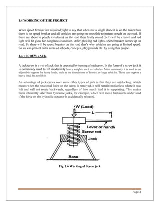
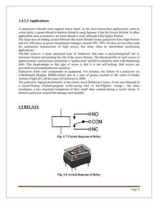
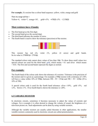
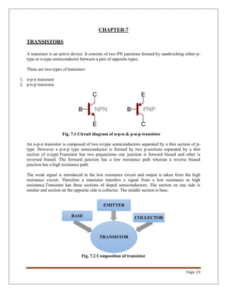
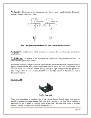
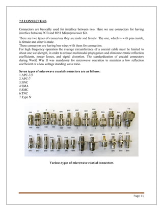
SlideShare a Scribd company logo
A Project Report on
“ADVANCED SPEED BREAKER”
Submitted in partial fulfilment of the requirement for Award of the Degree
Bachelors of Technology
In
Mechanical Engineering
Under The Guidance of
Er. ANS KHAN
(Assistant Prof.)
Submitted By
Asad Ahmad (1232140013)
Deepak Jindal (1232140020)
Ishant Gautam (1232140025)
Jawed Akhtar (1232140028)
Kafeel Ahmad (1232140030)
Department Of Mechanical Engineering
TRANSLAM INSTITUTE OF TECHNOLOGY & MANAGEMENT
(Dr. A.P.J Abdul Kalam Technical University, Lucknow)
(Batch: 2012-2016)
i
A Project Report on
“ADVANCED SPEED BREAKER”
Submitted in partial fulfilment of the requirement for Award of the Degree
Bachelors of Technology
In
Mechanical Engineering
Submitted By:
Under The Guidance of
Er. Anas Khan
(Assistant Prof.)
Asad Ahmad (1232140013)
Deepak Jindal (1232140020)
Ishant Gautam (1232140025)
Jawed Akhtar (1232140028)
Kafeel Ahmad (1232140030)
Department Of Mechanical Engineering
TRANSLAM INSTITUTE OF TECHNOLOGY & MANAGEMENT
(Dr. A.P.J Abdul Kalam Technical University, Lucknow)
(Batch: 2012-2016)
ii
DECLARATION
We hereby declare that the work, which is being presented in the project report,
entitled “Advanced Speed Breaker”. In the partial fulfillment for the award of
degree of “Bachelors of Technology” in department of Mechanical Engineering
and submitted to the Mechanical Engineering Department, Translam Institute of
Technology & Management affiliated to Dr. A.P.J Abdul Kalam Technical
University, Lucknow (U.P) is a record of our to own investigations carried under
the guidance of Er. Anas Khan, Assistant professor.
The matter of presented in the project has been submitted in any other
University/Institute for the award of Bachelors degree.
Signature: Signature:
Name: Asad Ahmad Name: Deepak Jindal
(Roll No.: 1232140013) (Roll No.: 1232140020)
Signature: Signature:
Ishant Gautam Jawed Akhtar
(Roll No.: 1232140025) (Roll No.: 1232140028)
Signature:
Kafeel Ahmad
(Roll No.: 1232140030)
iii
CERTIFICATE
This is to certify that Asad Ahmad (1232140013), Deepak Jindal (1232140020),
Ishant Gautam (1232140025), Jawed Akhtar (1232140028), Kafeel Ahmad
(1232140030) have carried out a project and study work on “Advanced Speed
Breaker” for the partial fulfillment of the award of the degree of Bachelors of
Technology in Mechanical Engineering in Translam Institute of Technology &
Management (Affiliated to Dr. A.P.J Abdul Kalam Technical University,
Lucknow) during the academic year 2012-2016.
Prof. Vikas Singh Er. Anas Khan
(H.O.D) (Project Guidance)
iv
ACKNOWLEDGEMENT
It gives us a great sense of pleasure to present the report of Advanced Speed
Breaker undertaken during B. Tech. Final Year. We owe special debt of gratitude
to Professor Anas Khan, Department of Mechanical Engineering, Translam
Institute Of Technology And Management, Meerut for his constant support and
guidance throughout the course of our work. His sincerity, thoroughness and
perseverance have been a constant source of inspiration for us. It is only his
cognizant efforts that our endeavors have seen light of the day.
We also take the opportunity to acknowledge the contribution of Professor Vikas
Singh, Head, Department of Mechanical Engineering, Translam Institute of
Technology And Management, Meerut for his full support and assistance during
the development of the project.
We also do not like to miss the opportunity to acknowledge the contribution of all
faculty members of the department for their kind assistance and cooperation
during the development of our project. Last but not the least, we acknowledge our
friends for their contribution in the completion of the project.
Asad Ahmad
Deepak Jindal
Ishant Gautam
Jawed Akhtar
Kafeel Ahmad
v
LIST OF FIGURES
Sl. No. TITLE OF FIGURE PAGE NO.
1.1 Wood structure 2
1.2 Screw jack 2
1.3 Relay 2
1.4 Buzzer 2
1.5 LEDs 2
1.6 Working of screw jack 4
1.7 Circuit diagram of relay 6
1.8 Actual diagram of relay 6
1.9 Stepper motor 8
1.10 Inside view of dc motor 8
2.1 Block diagram of microcontroller 9
2.2 Circuit diagram of capture mode 11
2.3 Circuit diagram of up and down counter 12
2.4 Circuit diagram of Baud Rate Generator 14
2.5 Circuit representation of Programmable Clock Out 16
3.1 Output characteristics of power down mode 16
3.2 AC characteristics 17
4.1 The ideal transformer as a circuit element 18
4.2 A step-down transformer 19
5.1 Schematic diagram of a bridge rectifier 20
vi
5.2 Output characteristics of rectifier 21
5.3 Bridge rectifier with smoothen output 22
5.4 Block diagram of voltage regulator 23
5.5 Internal block diagram of voltage regulator 24
6.1 Line diagram of fixed resistor 26
6.2 Colour coding of resistor 27
7.1 Circuit diagram of n-p-n & p-n-p transistor 29
7.2 Composition of transistor 29
7.3 Representation of emitter, base & collector in transistor 30
7.4 Heat sink 30
8.1 Representation of diode 33
8.2 Power diode & Signal diode 33
8.3 Line diagram of semiconductor diode 35
8.4 Line diagram of Zener diode 36
8.5 VI characteristics of Zener diode 36
9.1 Various types of Capacitor 37
9.2 Working of parallel plate capacitor 38
9.3 A simple demonstration of a parallel-plate capacitor 38
9.4 Circuit arrangement of capacitor and resistor 40
vii
LIST OF SYMBOLS
Fload force on the jack exerts by the load
Fin rotational force exerted on the handle of the jack
r length of the jack handle, from the screw axis to where the force is applied
l lead of the screw
V volt
mA milli ampere
MHz mega hertz
pF Pico farad
µF micro farad
IP Current in primary winding
IS Current in secondary winding
VP Induced emf in primary winding
VS Induced emf in secondary winding
NS Number of turns in secondary winding
NP Number of turns in primary winding
τ typical time constant
R resistance
C Capacitance
A ampere
 Ohm
W watt
Q Charge
E Electric field
D Plate separation
VC Charging voltage across the capacitor
IE Emitter current
IB Base current
IC Collector current
viii
LIST OF ABBREVIATIONS
COM Common
NC Normally Closed
NO Normally Open
BLDC Brushless DC electric motor
MMF Magneto motive force
EMF Electromotive force
AM Amplitude modulation
FM Frequency modulation
GVW Gross Vehicle Weight
SFR Special Function Register
I/O Input/output
RAM Random Access Memory
VHF Very High Frequency
UHF Ultra High Frequency
WRT with respect to
DCEN Down Counter Enable
ix
TABLE OF CONTENTS
PAGE
DECLARATION ……………………………………………………………………………….i
CERTIFICATE ...……………………………….……………………………...….....................ii
ACKNOWLEDGEMENT ……………………………………………………………….…….iii
LIST OF FIGURES ………………………………………………………………………….....iv
LIST OF SYMBOLS …………………………………………………………..……….………v
LIST OF ABBREVIATIONS ………………………………………………………….....…....vi
CHAPTER 1 INTRODUCTION …………………………………………………………….1-8
1.1 Aim of project ………………………………………………………...………....1
1.2 Hardware requirements ………………………………………………………....2
1.3 Block diagram ……………………………………………………………….......3
1.4 Working of the project ……………………………………………….……….... 4
1.4.1 Screw jack ……………………………………………….…....…4
1.4.1.1 Mechanical advantage ………….…………………..5
1.4.1.2 Limitations ………………………………….…........5
1.4.1.3 Applications ………………………………….……..6
1.5 Relays …………………………………………………………………………....6
1.6 DC motor ………………………………………………………………….……..7
1.6.1 Working of DC motor ……………………………………….….8
CHAPTER 2 MICROCONTROLLER ……………………………………………….……9-15
2.1 Features ……………………………………………………………………………......……..9
2.2 Special function resistors …………………………………………………………...….....…10
2.3 Interrupt resistors ……………………………………………………………........................10
2.3.1 Timer 0 & 1 ……………………………………………………….…...10
2.3.2 Timer 2 ………………………………………………………………...10
2.4 Capture mode ………………………………………………………………….…….….…...11
2.5 Auto-reload (Up or Down Counter) ……………………………………………….........…. 12
2.6 Baud rate generator ………………………………………………………………….………13
2.7 Programmable clock out ……………………………………………………………........… 14
2.8 Idle mode oscillator characteristics ……………………………………..………………......15
x
CHAPTER 3 POWER DOWN MODE …………………………………………………...16-17
3.1.1 AC characteristics ……………………………………………………………17
CHAPTER 4 TRANSFORMER ………………………………………………………… 18-19
4.1 Basic principle …………………………………………………………..........18
4.2 Transformer equation ………………………………………………………...19
CHAPTER 5 RECTIFIER ………………………………………………………………...20-25
5.1 Basic operation …………………………………………………………....… 20
5.2 Output smoothing …………………………………………………………...... 22
5.3 Bridge rectifier with smoothen output ……………………………………...…22
5.4 Voltage regulators …………………………………………………………..…23
5.4.1 Terminal fixed voltage regulator ……………………………..….......23
5.4.2 Internal block diagram …………..………………..…………....……..24
5.4.2.1 Features ……………………..…………..…………..…….….....……24
5.5 Crystal oscillator …………………………………………….………….…..…25
CHAPTER 6 RESISTOR ……………………………………………………………….…26-28
6.1 Types of resistors ………………………………………………………….....…26
6.1.1 Fixed resistors ……………………………………………….…..….26
6.2 Wire wound resistors ………………………………………….……. .27
6.2 Coding of resistors …………………………………..……………………...……27
6.2.1 Resistor colour chart ………………………………………….…......27
6.3 Variable resistors ………………………………………………………….….....28
CHAPTER 7 TRANSISTOR ………………………………………………………..……..29-31
7.1 Emitter ………………………………………………………………………….30
7.2 Base ……………………………………………………………………….……30
7.3 Collector …………………………………………………………….…..……...30
7.4 Heat sink ……………………………………………………………..………...30
7.5 Connectors …………………………………………………………...……..….31
CHAPTER 8 LED (LIGHT EMITTING DIODE) ………………………………...……..32-36
8.1 LED material ……………………………………………………………………32
8.2 Diode ……………………………………………………………………….…...33
xi
8.3 Some common diodes ………………………………………….…………….....34
8.3.1 Zener diode …………………………………………………...……....34
8.3.2 Photo diode ……………………………………………………………34
8.3.3 LED.………………………………………………...…………………34
8.4 Advantages of LED ………………………………………………………………..34
8.5 Semiconductor diode ………………………………………………………………35
8.6 Zener diode …………………………………………………………………...……36
CHAPTER 9 CAPACITOR ……………………………………………………………… 37-41
9.1 Theory of operation ………………………………………………………………38
9.2 Energy storage in capacitor ………………………………………….……….......39
9.3 current-voltage relation …………………………………………………………..39
9.4 DC circuit configuration …………………………………………..……………...40
CHAPTER 10 Specification of Maximum GVW by Govt. of India ……..……………...42-44
CHAPTER 11 CONCLUSION ……………………………………………….................……45
CHAPTER 12 Area of utility and future scope ……………………………………..……....46
References……………………………………………………………………………..………...47
Bibliography ………………………………………………………………………….………...48
xii
A
PROJECT REPORT
ON
ADVANCED SPEED BREAKER
ACTUAL VIEW OF PROJECT
Page 1
CHAPTER-1
INTRODUCTION
Energy from Advanced Speed Breaker is a wonderful project for every science student. This is a
very new concept to prevent the accidents and control the speed of vehicles. By using this model
we show the concept, how we can protect the accidents with the help of the speed breaker.
Having an automatic speed breaker on time demand using Embedded Systems tool; it an idea
which is very innovative and useful for the requirements of today’s speedy life.
The concept of the mentioned idea is to give the performance to vehicles as well as to make them
slow. The coding used in the completion of the research work is shown in the thesis. The real
working demo of the research work is very realistic and charming. This can be a very useful in
real life.
1.1 AIM OF PROJECT
In this project we use the automatic speed breaker to control the speed of vehicles at the time of
school and colleges. When the students come at the road, automatically the streets red light ON
for their fix time, then the speed breaker comes out on the road automatically. After the fix time
the breaker automatically gets OFF.
In the fast speed world, there are two perspectives, one is keeping speed and another is to
maintain safety mediums as well. So keeping speed is quite easy for a person and in case of
safety mediums, there must be a lot of attention. For safety purpose, preventing accidents on
road, there is a conventional method of having concrete speed breakers on road.
Page 2
1.2 HARDWARE REQUIREMENTS
1) Wood structure
2) Speed breaker
3) Screw jack
4) Relay
5) Controlling cards
6) BUZZER
7) LEDs
Fig. 1.1 Wood structure Fig. 1.2 Screw jack
Fig. 1.3 Relay Fig. 1.4 Buzzer
Fig. 1.5 LEDs
Page 3
1.3 BLOCK DIAGRAM
CONTROL UNIT
POWER SUPPLY
SENSOR
RED
LEDs
SCREW JACK TO
LIFT THE SPEED
BREAKER
SOUND
SYSTEM
Page 4
1.4 WORKING OF THE PROJECT
When speed breaker not required(right to say that when not a single student is on the road) then
there is no speed breaker and all vehicles are going on smoothly (constant speed) on the road. If
there are about to people (students) on the road then firstly sound (bell) will be created and red
light will be glow for dangerous condition. After glowing red lights, speed breaker comes up on
road. So there will be speed breaker on the road that’s why vehicles are going at limited speed.
So we can protect outer areas of schools, colleges, playgrounds etc. by using this project.
1.4.1 SCREW JACK
A jackscrew is a type of jack that is operated by turning a leadscrew. In the form of a screw jack it
is commonly used to lift moderately heavy weights, such as vehicles. More commonly it is used as an
adjustable support for heavy loads, such as the foundations of houses, or large vehicles. These can support a
heavy load, but not lift it.
An advantage of jackscrews over some other types of jack is that they are self-locking, which
means when the rotational force on the screw is removed, it will remain motionless where it was
left and will not rotate backwards, regardless of how much load it is supporting. This makes
them inherently safer than hydraulic jacks, for example, which will move backwards under load
if the force on the hydraulic actuator is accidentally released.
Fig. 1.6 Working of Screw jack
Page 5
1.4.1.1 Mechanical advantage
The mechanical advantage of a screw jack, the ratio of the force the jack exerts on the load to the
input force on the lever, ignoring frictionis
where,
is the force on the jack exerts by the load
is the rotational force exerted on the handle of the jack
is the length of the jack handle, from the screw axis to where the force is applied
is the lead of the screw.
This derives from two factors, the simple lever advantage of a long operating handle and also the
advantage of the inclined plane of the leadscrew. However, most screw jacks have large amounts
of friction which increase the input force necessary, so the actual mechanical advantage is often
only 30% to 50% of this figure.
1.4.1.2 Limitations
Screw jacks are limited in their lifting capacity. Increasing load increases friction within the
screw threads. A fine pitch thread, which would increase the advantage of the screw, also
reduces the size and strength of the threads. Longer operating levers soon reach a point where the
lever will simply bend at their inner end.
Screw jacks have now largely been replaced by hydraulic jacks. This was encouraged in 1858
when jacks by the Tangye company to Bramah's hydraulic press concept were applied to the
successful launching of Brunel's SS Great Britain, after two failed attempts by other means. The
maximum mechanical advantage possible for a hydraulic jack is not limited by the limitations on
screw jacks and can be far greater. After WWII, improvements to the grinding of hydraulic
rams and the use of O ring seals reduced the price of low-cost hydraulic jacks and they became
widespread for use with domestic cars. Screw jacks still remain for minimal cost applications,
such as the little-used tyre-changing jacks supplied with cars.
Page 6
1.4.1.3 Applications
A jackscrew's threads must support heavy loads. In the most heavy-duty applications, such as
screw jacks, a square thread or buttress thread is used, because it has the lowest friction. In other
application such as actuators, an Acme thread is used, although it has higher friction.
The large area of sliding contact between the screw threads means jackscrews have high friction
and low efficiency as power transmission linkages, around 30%–50%. So they are not often used
for continuous transmission of high power, but more often in intermittent positioning
applications.
The ball screw is a more advanced type of leadscrew that uses a recirculating-ball nut to
minimize friction and prolong the life of the screw threads. The thread profile of such screws is
approximately semicircular (commonly a "gothic arch" profile) to properly mate with thebearing
balls. The disadvantage to this type of screw is that it is not self-locking. Ball screws are
prevalent in powered leadscrew actuators.
Jackscrews form vital components in equipment. For instance, the failure of a jackscrew on
a McDonnell Douglas MD80 airliner due to a lack of grease resulted in the crash of Alaska
Airlines Flight 261 off the coast of California in 2000.
The jackscrew figured prominently in the classic novel Robinson Crusoe. It was also featured in
a recent History Channel program as the saving tool of the Pilgrims' voyage – the main
crossbeam, a key structural component of their small ship, cracked during a severe storm. A
farmer's jackscrew secured the damage until landfall.
1.5 RELAYS
Fig. 1.7 Circuit diagram of Relay
Fig. 1.8 Actual diagram of Relay
Page 7
A relay is an electrically operated switch. Current flowing through the coil of the relay creates a
magnetic field, which attracts a lever and changes the switch contacts. The coil current can be on
or off so relays have two switch positions and they are double throw (changeover) switches.
Relays allow one circuit to switch a second circuit that can be completely separate from the
first. For example a low voltage battery circuit can use a relay to switch a 230V AC mains
circuit. There is no electrical connection inside the relay between the two circuits, the link is
magnetic and mechanical.
The coil of a relay passes a relatively large current, typically 30mA for a 12V relay, but it
can be as much as 100mA for relays designed to operate from lower voltages. Most ICs
(chips) cannot provide this current and a transistor is usually used to amplify the small
IC current to the larger value required for the relay coil.
The maximum output current for the popular 555 timer IC is 200mA so these devices can supply
relay coils directly without amplification.
The relay's switch connections are usually labeled COM, NC and NO:
 COM = Common, always connect to this, it is the moving part of the switch.
 NC = Normally Closed, COM is connected to this when the relay coil is off.
 NO = Normally Open, COM is connected to this when the relay coil is on.
 Connect to COM and NO if you want the switched circuit to be on when the relay coil is on.
 Connect to COM and NC if you want the switched circuit to be on when the relay coil is off.
1.6 DC MOTOR
A DC motor is an electric motor that runs on direct current (DC) electricity.
Brushed
The brushed DC motor generates torque directly from DC power supplied to the motor by using
internal commutation, stationary permanent magnets, and rotating electrical magnets.It works on
the principle of Lorentz force , which states that any current carrying conductor placed within an
external magnetic field experiences a torque or force known as Lorentz force. Advantages of a
brushed DC motor include low initial cost, high reliability, and simple control of motor speed.
Disadvantages are high maintenance and low life-span for high intensity uses.
Synchronous
Synchronous DC motors, such as the brushless DC motor and the stepper motor, require external
commutation to generate torque. They lock up if driven directly by DC power. However, BLDC
motors are more similar to a synchronous ac motor.
Brushless
Brushless DC motors use a rotating permanent magnet in the rotor, and stationary electrical
magnets on the motor housing. A motor controller converts DC to AC. This design is simpler
Page 8
than that of brushed motors because it eliminates the complication of transferring power from
outside the motor to the spinning rotor. Advantages of brushless motors include long life span,
little or no maintenance, and high efficiency. Disadvantages include high initial cost, and more
complicated motor speed controllers.
Fig. 1.9 Stepper motor
1.6.1 Working of DC motor
In any electric motor, operation is based on simple electromagnetism. A current-carrying
conductor generates a magnetic field; when this is then placed in an external magnetic field, it
will experience a force proportional to the current in the conductor, and to the strength of the
external magnetic field. As you are well aware of from playing with magnets as a kid, opposite
(North and South) polarities attract, while like polarities (North and North, South and South)
repel. The internal configuration of a DC motor is designed to harness the magnetic interaction
between a current-carrying conductor and an external magnetic field to generate rotational
motion.
Fig. 1.10 Inside view of DC motor
Every DC motor has six basic parts -- axle, rotor, stator, commutator, field magnet(s), and
brushes. In most common DC motors, the external magnetic field is produced by high-strength
permanent magnets1
. The stator is the stationary part of the motor -- this includes the motor
casing, as well as two or more permanent magnet pole pieces. The rotor rotate with respect to the
stator. The rotor consists of windings (generally on a core), the windings being electrically
connected to the commutator. The above diagram shows a common motor layout -- with the
rotor inside the stator (field) magnets.
Page 9
CHAPTER-2
MICROCONTROLLER
(MICROCONTROLLER AT89C51/89s52)
2.1 Features:
• Compatible with MCS-51™ Products
• 8K Bytes of In-System Re programmable Flash Memory
• Endurance: 1,000 Write/Erase Cycles
• Fully Static Operation: 0 Hz to 24 MHz
• Three-level Program Memory Lock
• 256 x 8-bit Internal RAM
• 32 Programmable I/O Lines
•Three 16-bit Timer/Counters
• Eight Interrupt Sources
• Programmable Serial Channel
• Low-power Idle and Power-down Modes
Fig. 2.1 Block diagram of microcontroller
Page 10
2.2 Special Function Resistors
A map of the on-chip memory area called the Special Function Register (SFR) space is shown in
Table 1.
Note that not all of the addresses are occupied, and unoccupied addresses may not be
implemented on the chip. Read accesses to these addresses will in general return random data,
and write accesses will have an indeterminate effect. User software should not write 1s to these
unlisted locations, since they may be used in future prod new features. In that case, the reset or
inactive values of the new bits will always be 0.
2.3 Interrupt Resistors
The individual interrupt enable bits are in the IE register. Two priorities can be set for each of the
six interrupt sources in the IP register. Instructions that use indirect addressing access the upper
128 bytes of RAM. For example, the following indirect addressing instruction, where R0
contains 0A0H, accesses the data byte at address 0A0H, rather than P2 (whose address is 0A0H).
MOV @R0, #data
Note that stack operations are examples of indirect addressing, so the upper 128 bytes of data
RAM are avail available as stack space.
2.3.1 Timer 0 and 1
Timer 0 and Timer 1 in the AT89C52 operate the same way as Timer 0 and Timer 1 in the
T89C51.
2.3.2 Timer 2
Timer 2 is a 16-bit Timer/Counter that can operate as either a timer or an event counter. The type
of operation is selected by bit C/T2 in the SFR T2CON (shown in Table 2).Timer 2 has three
operating modes: capture, auto-reload (up or down counting), and baud rate generator. The
modes are selected by bits in T2CON, as shown in Table 3.Timer 2 consists of two 8-bit
registers, TH2 and TL2. In the Timer function, the TL2 register is incremented every machine
cycle. Since a machine cycle consists of 12 oscillator periods, the count rate is 1/12 of the
oscillator input pin, T2. In this function, the external input is sampled during S5P2 of every
machine cycle. When the samples show a high in one cycle and a low in the next cycle, the count
is incremented.
The new count value appears in the register during S3P1 of the cycle following the one in which
the transition was detected. Since two machine cycles (24 oscillator periods) are required to
recognize a 1-to-0 transition, the maximum count rate is 1/24 of the oscillator frequency. To
ensure that a given level is sampled at least once before it changes, the level should be held for at
least one full machine cycle.
Page 11
2.4 Capture Mode
In the capture mode, two options are selected by bit EXEN2 in T2CON. If EXEN2 = 0, Timer 2
is a 16-bit timer or counter which upon overflow sets bit TF2 in T2CON.This bit can then be
used to generate an interrupt. If EXEN2 = 1, Timer 2 performs the same operation, but a 1-to-0
transition at external input T2EX also causes the current value in TH2 and TL2 to be captured
into CAP2H and RCAP2L, respectively. In addition, the transition at T2EX causes bit EXF2 in
T2CON to be set. The EXF2 bit, like TF2, can generate an interrupt. The capture mode is
illustrated in Figure 2.2.
Fig. 2.2 Circuit diagram of capture mode
Page 12
2.5 Auto-reload (Up or Down Counter)
Timer 2 can be programmed to count up or down when configured in its 16-bit auto-reload
mode. This feature is invoked by the DCEN (Down Counter Enable) bit located in the SFR
T2MOD (see Table 4). Upon reset, the DCEN bit is set to 0 so that timer 2 will default to count
up. When DCEN is set, Timer 2 can count up or down, depending on the value of the T2EX pin.
Figure 2 shows Timer 2 automatically counting up when DCEN = 0. In this mode, two options
are selected by bitEXEN2 in T2CON. If EXEN2 = 0, Timer 2 counts up to 0FFFFH and then
sets the TF2 bit upon overflow. The overflow also causes the timer registers to be reloaded with
the 16-bit value in RCAP2H and RCAP2L. The values in Timer in Capture ModeRCAP2H and
RCAP2L are preset by software. If EXEN2 = 1, a 16-bit reload can be triggered either by an
overflow or by a 1-to-0 transition at external input T2EX. This transition also sets the EXF2 bit.
Both the TF2 and EXF2 bits can generate an interrupt if enabled. Setting the DCEN bit enables
Timer 2 to count up or down, as shown in Figure 3. In this mode, the T2EX pin controls the
direction of the count. A logic 1 at T2EX makes Timer 2 count up. The timer will overflow at
0FFFFH and set the TF2 bit. This overflow also causes the 16-bit value in RCAP2H and
RCAP2L to be reloaded into the timer registers, TH2 and TL2, respectively. A Logic 0 at T2EX
makes Timer 2 count down. The timer underflows when TH2 and TL2 equal the values stored in
RCAP2H and RCAP2L. The underflow sets the TF2 bit and causes 0FFFFH to be reloaded into
the timer Registers. The EXF2 bit toggles whenever Timer 2 overflows or underflows and can be
used as a 17th bit of resolution. In this operating mode, EXF2 does not flag an interrupt.
Fig. 2.3 Circuit diagram of up and down counter
Page 13
2.6 Baud Rate Generator
Timer 2 is selected as the baud rate generator by setting TCLK and/or RCLK in T2CON (Table
2). Note that the baud rates for transmit and receive can be different if Timer 2 is used for the
receiver or transmitter and Timer 1 is used for the other function. Setting RCLK and/or TCLK
puts Timer 2 into its baud rate generator mode, as shown in Figure4. The baud rate generator
mode is similar to the auto-reload mode, in that a rollover in TH2 causes the Timer 2 registers to
be reloaded with the 16-bit value in registers RCAP2H and RCAP2L, which are preset by
software.
The baud rates in Modes 1 and 3 are determined by Timer2’s overflow rate according to the
following equation.
The Timer can be configured for either timer or counter operation. In most applications, it is
configured for timer operation (CP/T2 = 0). The timer operation is different for Timer 2 when it
is used as a baud rate generator. Normally, as a timer, it increments every machine cycle (at 1/12
the oscillator frequency).As a baud rate generator, however, it increments every state time (at 1/2
the oscillator frequency).
The baud rate formula is given below.
Where (RCAP2H, RCAP2L) is the content of RCAP2H and RCAP2L taken as a 16-bit unsigned
integer. Timer 2 as a baud rate generator is shown in Figure 4. This figure is valid only if RCLK
or TCLK = 1 in T2CON. Note that a rollover in TH2 does not set TF2 and will not generate an
interrupt. Note too, that if EXEN2 is set, a 1-to-0 transition in T2EX will set EXF2 but will not
cause a reload from (RCAP2H, RCAP2L) to (TH2, TL2). Thus when Timer 2 is in use as a baud
rate generator, T2EX can be used as an extra external interrupt.
Note that when Timer 2 is running (TR2 = 1) as a timer in the baud rate generator mode, TH2 or
TL2 should not be read from or written to. Under these conditions, the Timer is incremented
every state time, and the results of a read or write may not be accurate. The RCAP2 registers
may be read but should not be written to, because a write might overlap a reload and cause write
and/or reload errors. The timer should be turned off (clear TR2) before accessing the Timer 2 or
RCAP2 registers.
Page 14
Fig. 2.4 Circuit diagram of Baud Rate Generator
2.7 Programmable Clock Out
A 50% duty cycle clock can be programmed to come out on P1.0, as shown in Figure 5. This pin,
besides being a regular I/O pin, has two alternate functions. It can be programmed to input the
external clock for Timer/Counter 2 or to output a 50% duty cycle clock ranging from 61 Hz to 4
MHz at a 16 MHz operating frequency. To configure the Timer/Counter 2 as a clock generator,
bit C/T2 (T2CON.1) must be cleared and bit T2OE (T2MOD.1) must be set. Bit TR2 (T2CON.2)
starts and stops the timer. The clock-out frequency depends on the oscillator frequency and the
reload value of Timer 2 capture registers (RCAP2H, RCAP2L), as shown in the following
equation.
In the clock-out mode, Timer 2 roll-overs will not generate an interrupt. This behavior is similar
to when Timer 2 is used as a baud-rate generator. It is possible to use Timer 2 as a baud-rate
generator and a clock generator simultaneously. Note, however, that the baud-rate and clock-out
Frequencies cannot be determined independently from one another since they both use RCAP2H
and RCAP2L.
Page 15
Fig. 2.5 Circuit representation of Programmable Clock Out
2.8 Idle Mode Oscillator Characteristics
XTAL1 and XTAL2 are the input and output, respectively, of an inverting amplifier that can be
configured for use as an on-chip oscillator, as shown in Figure 7. Either a quartz crystal or
ceramic resonator may be used. To drive the device from an external clock source, XTAL2
should be left
Un connected while XTAL1 is driven, as shown in Figure 8.There are no requirements on the
duty cycle of the external clock signal, since the input to the internal clocking circuitry is through
a divide-by-two flip-flop, but minimum and maximum voltage high and low time specifications
must be observed.
In idle mode, the CPU puts itself to sleep while all the on chip peripherals remain active. The
mode is invoked by software. The content of the on-chip RAM and all the special functions
registers remain unchanged during this mode. The idle mode can be terminated by any enabled
interrupt or by a hardware reset.
Note that when idle mode is terminated by a hardware reset, the device normally resumes
program execution from where it left off, up to two machine cycles before the internal reset
algorithm takes control. On-chip hardware inhibits access to internal RAM in this event, but
access to the port pins is not inhibited. To eliminate the possibility of an unexpected write to a
port pin when idle mode is terminated by a reset, the instruction following the one that invokes
idle mode should not write to a port pin or to external memory.
Page 16
CHAPTER-3
3.1 POWER DOWN MODE
In the power-down mode, the oscillator is stopped, and the instruction that invokes power-down
is the last instruction executed. The on-chip RAM and Special Function Registers retain their
values until the power-down mode is terminated. The only exit from power-down is a hardware
reset. Reset redefines the SFR s but does not change the on-chip RAM. The reset should not be
cultivated before VCC is restored to its normal operating level and must be held active long
enough to allow the oscillator to restart and stabilize.
Fig. 3.1 Output characteristics of power down mode
Page 17
3.1.1 AC Characteristics
Under operating conditions, load capacitance for Port 0, ALE/PROG, and PSEN = 100 pF; load
capacitance for all otheroutputs = 80 Pf.
Fig. 3.2 AC characteristics
Page 18
CHAPTER-4
4.1 TRANSFORMERS
A transformer is a device that transfers electrical energy from one circuit to another by magnetic
coupling without requiring relative motion between its parts. It usually comprises two or more
coupled windings, and, in most cases, a core to concentrate magnetic flux. A transformer
operates from the application of an alternating voltage to one winding, which creates a time-
varying magnetic flux in the core. This varying flux induces a voltage in the other windings.
Varying the relative number of turns between primary and secondary windings determines the
ratio of the input and output voltages, thus transforming the voltage by stepping it up or down
between circuits.
4.1.1 Basic principle
The principles of the transformer are illustrated by consideration of a hypothetical ideal
transformer consisting of two windings of zero resistance around a core of negligible reluctance.
A voltage applied to the primary winding causes a current, which develops a magnetomotive
force (MMF) in the core. The current required to create the MMF is termed the magnetising
current; in the ideal transformer it is considered to be negligible. The MMF drives flux around
the magnetic circuit of the core.
Fig. 4.1 The ideal transformer as a circuit element
An electromotive force (EMF) is induced across each winding, an effect known as mutual
inductance. The windings in the ideal transformer have no resistance and so the EMFs are equal
in magnitude to the measured terminal voltages. In accordance with Faraday's law of induction,
they are proportional to the rate of change of flux:
and
Page 19
EMF induced in primary and secondary windings
where:
and are the induced EMFs across primary and secondary windings,
aVnd are the numbers of turns in the primary and secondary windings,
and are the time derivatives of the flux linking the primary and secondary windings.
In the ideal transformer, all flux produced by the primary winding also links the secondary, and
so , from which the well-known transformer equation follows:
4.1.2 Transformer Equation
The ratio of primary to secondary voltage is therefore the same as the ratio of the number of
turns; alternatively, that the volts-per-turn is the same in both windings. The conditions that
determine Transformer working in STEP UP or STEP DOWN mode are:
Ns > Np
Fig. 4.2 A step-down transformer
Page 20
CHAPTER-5
RECTIFIER
A bridge rectifier is an arrangement of four diodes connected in a bridge circuit as shown
below, that provides the same polarity of output voltage for any polarity of the input voltage.
When used in its most common application, for conversion of alternating current (AC) input into
direct current (DC) output, it is known as a bridge rectifier. The bridge rectifier provides full
wave rectification from a two wire AC input (saving the cost of a center tapped transformer) but
has two diode drops rather than one reducing efficiency over a center tap based design for the
same output voltage.
Fig. 5.1 Schematic diagram of a bridge rectifier
The essential feature of this arrangement is that for both polarities of the voltage at the bridge
input, the polarity of the output is constant.
5.1 Basic Operation
When the input connected at the left corner of the diamond is positive with respect to the one
connected at the right hand corner, current flows to the right along the upper colored path to the
output, and returns to the input supply via the lower one.
Page 21
When the right hand corner is positive relative to the left hand corner, current flows along the
upper colored path and returns to the supply via the lower colored path.
Fig. 5.2 Output characteristics of rectifier
In each case, the upper right output remains positive with respect to the lower right one. Since
this is true whether the input is AC or DC, this circuit not only produces DC power when
supplied with AC power: it also can provide what is sometimes called "reverse polarity
protection". That is, it permits normal functioning when batteries are installed backwards or DC
input-power supply wiring "has its wires crossed" (and protects the circuitry it powers against
damage that might occur without this circuit in place).
Prior to availability of integrated electronics, such a bridge rectifier was always constructed from
discrete components. Since about 1950, a single four-terminal component containing the four
diodes connected in the bridge configuration became a standard commercial component and is
now available with various voltage and current ratings.
Page 22
5.2 Output Smoothing
For many applications, especially with single phase AC where the full-wave bridge serves to
convert an AC input into a DC output, the addition of a capacitor may be important because the
bridge alone supplies an output voltage of fixed polarity but pulsating magnitude.
Fig. 5.3 Bridge rectifier with smoothen output
5.3 Bridge Rectifier with smoothen output
The function of this capacitor, known as a 'smoothing capacitor' is to lessen the variation in (or
'smooth') the raw output voltage waveform from the bridge. One explanation of 'smoothing' is
that the capacitor provides a low impedance path to the AC component of the output, reducing
the AC voltage across, and AC current through, the resistive load. In less technical terms, any
drop in the output voltage and current of the bridge tends to be cancelled by loss of charge in the
capacitor. This charge flows out as additional current through the load. Thus the change of load
current and voltage is reduced relative to what would occur without the capacitor. Increases of
voltage correspondingly store excess charge in the capacitor, thus moderating the change in
output voltage / current.
The capacitor and the load resistance have a typical time constant τ = RC where C and R are the
capacitance and load resistance respectively.
As long as the load resistor is large enough so that this time constant is much longer than the
time of one ripple cycle, the above configuration will produce a well smoothed DC voltage
across the load resistance. In some designs, a series resistor at the load side of the capacitor is
added. The smoothing can then be improved by adding additional stages of capacitor–resistor
pairs, often done only for sub-supplies to critical high-gain circuits that tend to be sensitive to
supply voltage noise.
Page 23
5.4 Voltage Regulators
A voltage regulator is an electrical regulator designed to automatically maintain a constant
voltage level. It may use an electromechanical mechanism, or passive or active electronic
components. Depending on the design, it may be used to regulate one or more AC or DC
voltages. With the exception of shunt regulators, all voltage regulators operate by comparing the
actual output voltage to some internal fixed reference voltage. Any difference is amplified and
used to control the regulation element. This forms a negative feedbackservo control loop. If the
output voltage is too low, the regulation element is commanded to produce a higher voltage. For
some regulators if the output voltage is too high, the regulation element is commanded to
produce a lower voltage; however, many just stop sourcing current and depend on the current
draw of whatever it is driving to pull the voltage back down. In this way, the output voltage is
held roughly constant. The control loop must be carefully designed to produce the desired
tradeoff between stability and speed of response.
5.4.1 LM7805 (3-Terminal Fixed Voltage Regulator)
The MC78XX/LM78XX/MC78XXA series of three terminal positive regulators are available in
the
TO-220/D-PAK package and with several fixed output voltages, making them useful in a wide
range of applications. Each type employs internal current limiting, thermal shut down and safe
operating area protection, making it essentially indestructible. If adequate heat sinking is
provided, they can deliver over 1A output current. Although designed primarily as fixed voltage
regulators, these devices can be used with external components to obtain adjustable voltages and
currents.
Fig. 5.4 Block diagram of voltage regulator
Page 24
5.4.2 Internal block Diagram
Fig. 5.5 Internal block diagram of voltage regulator
5.4.2.1 Features:
• Output Current up to 1A
• Output Voltages of 5, 6, 8, 9, 10, 12, 15, 18, 24V
• Thermal Overload Protection
• Short Circuit Protection
• Output Transistor Safe Operating Area Protection
Page 25
5.5 CRYSTAL OSCILLATOR
It is often required to produce a signal whose frequency or pulse rate is very stable and exactly
known. This is important in any application where anything to do with time or exact
measurement is crucial. It is relatively simple to make an oscillator that produces some sort of a
signal, but another matter to produce one of relatively precise frequency and stability. AM radio
stations must have a carrier frequency accurate within 10Hz of its assigned frequency, which
may be from 530 to 1710 kHz. SSB radio systems used in the HF range (2-30 MHz) must be
within 50 Hz of channel frequency for acceptable voice quality, and within 10 Hz for best
results. Some digital modes used in weak signal communication may require frequency stability
of less than 1 Hz within a period of several minutes. The carrier frequency must be known to
fractions of a hertz in some cases. An ordinary quartz watch must have an oscillator accurate to
better than a few parts per million. One part per million will result in an error of slightly less than
one half second a day, which would be about 3 minutes a year. This might not sound like much,
but an error of 10 parts per million would result in an error of about a half an hour per year. A
clock such as this would need resetting about once a month, and more often if you are the
punctual type. A programmed VCR with a clock this far off could miss the recording of part of a
TV show. Narrow band SSB communications at VHF and UHF frequencies still need 50 Hz
frequency accuracy. At 440 MHz, this is slightly more than 0.1 part per million.
Ordinary L-C oscillators using conventional inductors and capacitors can achieve typically 0.01
to 0.1 percent frequency stability, about 100 to 1000 Hz at 1 MHz. This is OK for AM and FM
broadcast receiver applications and in other low-end analog receivers not requiring high tuning
accuracy. By careful design and component selection, and with rugged mechanical construction,
.01 to 0.001%, or even better (.0005%) stability can be achieved. The better figures will
undoubtedly employ temperature compensation components and regulated power supplies,
together with environmental control (good ventilation and ambient temperature regulation) and
“battleship” mechanical construction. This has been done in some communications receivers
used by the military and commercial HF communication receivers built in the 1950-1965 era,
before the widespread use of digital frequency synthesis. But these receivers were extremely
expensive, large, and heavy. Many modern consumer grade AM, FM, and shortwave receivers
employing crystal controlled digital frequency synthesis will do as well or better from a
frequency stability standpoint.
An oscillator is basically an amplifier and a frequency selective feedback network (Fig 1). When,
at a particular frequency, the loop gain is unity or more, and the total phaseshift at this frequency
is zero, or some multiple of 360 degrees, the condition for oscillation is satisfied, and the circuit
will produce a periodic waveform of this frequency. This is usually a sine wave, or square wave,
but triangles, impulses, or other waveforms can be produced. In fact, several different waveforms
often are simultaneously produced by the same circuit, at different points. It is also possible to
have several frequencies produced as well, although this is generally undesirable.
Page 26
CHAPTER-6
RESISTOR
6.1 TYPES OF RESISTORS
Resistors are used to limit the value of current in a circuit. Resistors offer opposition to the flow
of current. They are expressed in ohms for which the symbol is ‘’. Resistors are broadly
classified as
(1) Fixed Resistors
(2) Variable Resistors
6.1.1 FIXED RESISTORS
The most common of low wattage, fixed type resistors is the molded-carbon composition
resistor. The resistive material is of carbon clay composition. The leads are made of tinned
copper. Resistors of this type are readily available in value ranging from few ohms to about
20M, having a tolerance range of 5 to 20%. They are quite inexpensive. The relative size of all
fixed resistors changes with the wattage rating.
Another variety of carbon composition resistors is the metalized type. It is made by deposition a
homogeneous film of pure carbon over a glass, ceramic or other insulating core. This type of
film-resistor is sometimes called the precision type, since it can be obtained with an accuracy of
1%.
Lead Tinned Copper Material
Colour Coding Molded Carbon Clay Composition
Fig. 6.1 Line diagram of fixed resistor
Page 27
6.1.2 A WIRE WOUND RESISTOR
It uses a length of resistance wire, such as nichrome. This wire is wounded on to a round hollow
porcelain core. The ends of the winding are attached to these metal pieces inserted in the core.
Tinned copper wire leads are attached to these metal pieces. This assembly is coated with an
enamel coating powdered glass. This coating is very smooth and gives mechanical protection to
winding. Commonly available wire wound resistors have resistance values ranging from 1 to
100K, and wattage rating up to about 200W.
6.2 CODING OF RESISTOR
Some resistors are large enough in size to have their resistance printed on the body. However
there are some resistors that are too small in size to have numbers printed on them. Therefore, a
system of colour coding is used to indicate their values. For fixed, moulded composition resistor
four colour bands are printed on one end of the outer casing. The colour bands are always read
left to right from the end that has the bands closest to it. The first and second band represents the
first and second significant digits, of the resistance value. The third band is for the number of
zeros that follow the second digit. In case the third band is gold or silver, it represents a
multiplying factor of 0.1to 0.01. The fourth band represents the manufacture’s tolerance.
6.2.1 RESISTOR COLOUR CHART
Fig. 6.2 Colour coding of resistor
5 green
0 black
1 brown
2 red
3 orange
4 yellow
6 blue
7 purple
8 silver
9 white
0 black
1 brown
2 red
3 orange
4 yellow
6 blue
7 purple
8 silver
9 white
5green 5 green
0 black
1 brown
2 red
3 orange
4 yellow
6 blue
7 purple
8 silver
9 white
5 green
0 black
1 brown
2 red
3 orange
4 yellow
6 blue
7 purple
8 silver
9 white
Page 28
For example, if a resistor has a colour band sequence: yellow, violet, orange and gold
Then its range will be—
Yellow=4, violet=7, orange=10³, gold=±5% =47KΏ ±5% =2.35KΏ
Most resistors have 4 bands:
 The first band gives the first digit.
 The second band gives the second digit.
 The third band indicates the number of zeros.
 The fourth band is used to show the tolerance (precision) of the resistor.
This resistor has red (2), violet (7), yellow (4 zeros) and gold bands.
So its value is 270000 = 270 k .
The standard colour code cannot show values of less than 10 . To show these small values two
special colours are used for the third band: gold, which means × 0.1 and silver which means
× 0.01. The first and second bands represent the digits as normal.
For example:
The fourth band of the colour code shows the tolerance of a resistor. Tolerance is the precision of
the resistor and it is given as a percentage. For example a 390 resistor with a tolerance of ±10%
will have a value within 10% of 390 , between 390 - 39 = 351 and 390 + 39 = 429 (39 is
10% of 390).
A special colour code is used for the fourth band tolerance: silver ±10%, gold ±5%, red
±2%, brown ±1%. If no fourth band is shown the tolerance is ±20%.
6.3 VARIABLE RESISTOR
In electronic circuits, sometimes it becomes necessary to adjust the values of currents and
voltages. For n example it is often desired to change the volume of sound, the brightness of a
television picture etc. Such adjustments can be done by using variable resistors.
Although the variable resistors are usually called rheostats in other applications, the smaller
variable resistors commonly used in electronic circuits are called potentiometers.
Page 29
CHAPTER-7
TRANSISTORS
A transistor is an active device. It consists of two PN junctions formed by sandwiching either p-
type or n-type semiconductor between a pair of opposite types.
There are two types of transistor:
1. n-p-n transistor
2. p-n-p transistor
Fig. 7.1 Circuit diagram of n-p-n & p-n-p transistor
An n-p-n transistor is composed of two n-type semiconductors separated by a thin section of p-
type. However a p-n-p type semiconductor is formed by two p-sections separated by a thin
section of n-type.Transistor has two pnjunctions one junction is forward biased and other is
reversed biased. The forward junction has a low resistance path whereas a reverse biased
junction has a high resistance path.
The weak signal is introduced in the low resistance circuit and output is taken from the high
resistance circuit. Therefore a transistor transfers a signal from a low resistance to high
resistance.Transistor has three sections of doped semiconductors. The section on one side is
emitter and section on the opposite side is collector. The middle section is base.
Fig. 7.2 Composition of transistor
TRANSISTOR
BASE
EMITTER
COLLECTOR
Page 30
7.1 Emitter: The section on one side that supplies charge carriers is called emitter. The emitter
is always forward biased w.r.t. base.
Fig. 7.3 Representation of emitter, base & collector in transistor
7.2 Base: The middle section which forms two pn-junctions between the emitter and collector
is called base.
7.3 Collector: The section on the other side that collects the charge is called collector. The
collector is always reversed biased.
A transistor raises the strength of a weak signal and thus acts as an amplifier. The weak signal is
applied between emitter-base junction and output is taken across the load Rc connected in the
collector circuit. The collector current flowing through a high load resistance RC produces a
large voltage across it. Thus a weak signal applied in the input appears in the amplified form in
the collector circuit.
7.4 Heat sink
Fig. 7.4 Heat sink
Waste heat is produced in transistors due to the current flowing through them. Heat sinks are
needed for power transistors because they pass large currents. If you find that a transistor is
becoming too hot to touch it certainly needs a heat sink! The heat sink helps to dissipate
(remove) the heat by transferring it to the surrounding air.
Page 31
7.5 CONNECTORS
Connectors are basically used for interface between two. Here we use connectors for having
interface between PCB and 8051 Microprocessor Kit.
There are two types of connectors they are male and female. The one, which is with pins inside,
is female and other is male.
These connectors are having bus wires with them for connection.
For high frequency operation the average circumference of a coaxial cable must be limited to
about one wavelength, in order to reduce multimodal propagation and eliminate erratic reflection
coefficients, power losses, and signal distortion. The standardization of coaxial connectors
during World War II was mandatory for microwave operation to maintain a low reflection
coefficient or a low voltage standing wave ratio.
Seven types of microwave coaxial connectors are as follows:
1.APC-3.5
2.APC-7
3.BNC
4.SMA
5.SMC
6.TNC
7.Type N
Various types of microwave coaxial connectors
Page 32
CHAPTER-8
LED (LIGHT EMITTING DIODE)
A junction diode, such as LED, can emit light or exhibit electro luminescence. Electro
luminescence is obtained by injecting minority carriers into the region of a pn junction where
radiative transition takes place. In radiative transition, there is a transition of electron from the
conduction band to the valence band, which is made possibly by emission of a photon. Thus,
emitted light comes from the hole electron recombination. What is required is that electrons
should make a transition from higher energy level to lower energy level releasing photon of
wavelength corresponding to the energy difference associated with this transition. In LED the
supply of high-energy electron is provided by forward biasing the diode, thus injecting electrons
into the n-region and holes into p-region.
The pn junction of LED is made from heavily doped material. On forward bias condition,
majority carriers from both sides of the junction cross the potential barrier and enter the opposite
side where they are then minority carrier and cause local minority carrier population to be larger
than normal. This is termed as minority injection. These excess minority carrier diffuse away
from the junction and recombine with majority carriers. In LED, every injected electron takes
part in a radiative recombination and hence gives rise to an emitted photon. Under reverse bias
no carrier injection takes place and consequently no photon is emitted. For direct transition from
conduction band to valence band the emission wavelength.
In practice, every electron does not take part in radiative recombination and hence, the efficiency
of the device may be described in terms of the quantum efficiency which is defined as the rate of
emission of photons divided by the rate of supply of electrons. The number of radiative
recombination, that take place, is usually proportional to the carrier injection rate and hence to
the total current flowing.
8.1 LED Materials
One of the first materials used for LED is GaAs. This is a direct band gap material, i.e., it
exhibits very high probability of direct transition of electron from conduction band to valence
band. GaAs has E= 1.44 eV. This works in the infrared region.
GaP and GaAsP are higher band gap materials. Gallium phosphide is an indirect band gap
semiconductor and has poor efficiency because band to band transitions are not normally
observed.
Gallium Arsenide Phosphide is a tertiary alloy. This material has a special feature in that it
changes from being direct band gap material.
Blue LEDs are of recent origin. The wide band gap materials such as GaN are one of the most
promising LEDs for blue and green emission. Infrared LEDs are suitable for optical coupler
applications.
Page 33
8.2 DIODE
The simplest semiconductor device is made up of a sandwich of P-type semi-conducting
material, with contacts provided to connect the p-and n-type layers to an external circuit.
This is a junction Diode. If the positive terminal of the battery is connected to the p-type
material (cathode) and the negative terminal to the N-type material (Anode), a large current
will flow. This is called forward Current or forward biased.
If the connections are reversed, a very little current will flow. This is because under this
condition, the p-type material will accept the electron from the negative terminal of the
battery and the N-type material will give up its free electrons to the battery, resulting in
the state of electrical equilibrium since the N-type material has no more electrons. Thus
there will be a small current to flow and the diode is called Reverse biased. Thus the
Diode allows direct current to pass only in one direction while blocking it is the other
direction. Power diodes are used in concerting AC into DC. In this , current will flow freely
during the first half cycle (forward biased) and practically not at all during the other half
cycle (reverse biased). This makes the diode an effective rectifier, which convert ac into
pulsating dc. Signal diodes are used in radio circuits for detection. Zener diodes are used in
the circuit to control the voltage.
Fig. 8.1 Representation of diode
Fig. 8.2 Power diode & Signal diode
Page 34
8.3 Some common diodes
1. Zener diode.
2. Photo diode.
3.Light Emitting diode.
8.3.1 ZENER DIODE
A zener diode is specially designed junction diode, which can operate continuously without
being damaged in the region of reverse break down voltage. One of the most important
applications of zener diode is the design of constant voltage power supply. The zener diode is
joined in reverse bias to d.c. through a resistance R of suitable value.
8.3.2 PHOTO DIODE
A photo diode is a junction diode made from photo- sensitive semiconductor or material. In such
a diode, there is a provision to allow the light of suitable frequency to fall on the p-n junction. It
is reverse biased, but the voltage applied is less than the break down voltage. As the intensity of
incident light is increased, current goes on increasing till it becomes maximum. The maximum
current is called saturation current.
8.3.3 LIGHT EMITTING DIODE (LED)
When a junction diode is forward biased, energy is released at the junction diode is forward
biased, energy is released at the junction due to recombination of electrons and holes. In case of
silicon and germanium diodes, the energy released is in infrared region. In the junction diode
made of gallium arsenate or indium phosphide, the energy is released in visible region. Such a
junction diode is called a light emitting diode or LED.
8.4 ADVANTAGES OF LEDs
1.Low operating voltage, current, and power consumption makes Leds compatible with
electronic drive circuits. This also makes easier interfacing as compared to filament incandescent
and electric discharge lamps.
2.The rugged, sealed packages developed for LEDs exhibit high resistance to mechanical shock
and vibration and allow LEDs to be used in severe environmental conditions where other light
sources would fail.
3.LED fabrication from solid-state materials ensures a longer operating lifetime, thereby
improving overall reliability and lowering maintenance costs of the equipment in which they are
installed.
4.The range of available LED colours-from red to orange, yellow, and green-provides the
designer with added versatility.
Page 35
LEDs have certain limitations such as:
1. Temperature dependence of radiant output power and wave length.
2. Sensitivity to damages by over voltage or over current.
3. Theoretical overall efficiency is not achieved except in special cooled or pulsed conditions.
There are also two different types of diodes:-
8.5 SEMICONDUCTOR DIODE
A PN junctions is known as a semiconductor or crystal diode.A crystal diode has two terminal
when it is connected in a circuit one thing is decide is weather a diode is forward or reversed
biased. There is a easy rule to ascertain it. If the external CKT is trying to push the conventional
current in the direction of error, the diode is forward biased. One the other hand if the
conventional current is trying is trying to flow opposite the error head, the diode is reversed
biased putting in simple words.
Fig. 8.3 Line diagram of semiconductor diode
8.5.1 Characteristics of Semiconductor diode
1.If arrowhead of diode symbol is positive W.R.T Bar of the symbol, the diode is forward biased.
2.The arrowhead of diode symbol is negative W.R.T bar , the diode is the reverse bias.
When we used crystal diode it is often necessary to know that which end is arrowhead and which
end is bar. So following method are available.
3.Some manufactures actually point the symbol on the body of the diode e. g By127 by 11 4
crystal diode manufacture by b e b.
4.Sometimes red and blue marks are on the body of the crystal diode. Red mark do not arrow
where’s blue mark indicates bar e .g oa80 crystal diode.
Page 36
8.6 ZENER DIODE
It has been already discussed that when the reverse bias on a crystal diode is increased a critical
voltage, called break down voltage. The break down or zener voltage depends upon the amount
of doping. If the diode is heavily doped depletion layer will be thin and consequently the break
down of he junction will occur at a lower reverse voltage. On the other hand, a lightly doped
diode has a higher break down voltage, it is called zener diode.
Fig. 8.4 Line diagram of Zener diode
Fig. 8.5 VI characteristics of Zener diode
Page 37
CHAPTER-9
CAPACITOR
A capacitor or condenser is a passive electronic component consisting of a pair of conductors
separated by a dielectric (insulator). When a potential difference (voltage) exists across the
conductors, an electric field is present in the dielectric. This field stores energy and produces a
mechanical force between the conductors. The effect is greatest when there is a narrow
separation between large areas of conductor; hence capacitor conductors are often called plates.
An ideal capacitor is characterized by a single constant value, capacitance, which is measured in
farads. This is the ratio of the electric charge on each conductor to the potential difference
between them. In practice, the dielectric between the plates passes a small amount of leakage
current. The conductors and leads introduce an equivalent series resistance and the dielectric has
an electric field strength limit resulting in a breakdown voltage.
Capacitors are widely used in electronic circuits to block the flow of direct current while
allowing alternating current to pass, to filter out interference, to smooth the output of power
supplies, and for many other purposes. They are used in resonant circuits in radio frequency
equipment to select particular frequencies from a signal with many frequencies
Fig. 9.1 Various types of Capacitor
Page 38
9.1 THEORY OF OPERATION
Fig. 9.2 Working of parallel plate capacitor
Charge separation in a parallel-plate capacitor causes an internal electric field. A dielectric
(orange) reduces the field and increases the capacitance.
Fig. 9.3 A simple demonstration of a parallel-plate capacitor
A capacitor consists of two conductors separated by a non-conductive region. The non-
conductive substance is called the dielectric medium, although this may also mean a vacuum or a
semiconductordepletion region chemically identical to the conductors. A capacitor is assumed to
be self-contained and isolated, with no net electric charge and no influence from an external
electric field. The conductors thus contain equal and opposite charges on their facing surfaces,
and the dielectric contains an electric field. The capacitor is a reasonably general model for
electric fields within electric circuits.
Page 39
An ideal capacitor is wholly characterized by a constant capacitance C, defined as the ratio of
charge ±Q on each conductor to the voltage V between them
Sometimes charge buildup affects the mechanics of the capacitor, causing the capacitance to
vary. In this case, capacitance is defined in terms of incremental changes:
In SI units, a capacitance of one farad means that one coulomb of charge on each conductor
causes a voltage of one volt across the device.
9.2 Energy storage in capacitor
Work must be done by an external influence to move charge between the conductors in a
capacitor. When the external influence is removed, the charge separation persists and energy is
stored in the electric field. If charge is later allowed to return to its equilibrium position, the
energy is released. The work done in establishing the electric field, and hence the amount of
energy stored, is given by:
9.3 Current-voltage relation
The current i(t) through a component in an electric circuit is defined as the rate of change of the
charge q(t) that has passed through it. Physical charges cannot pass through the dielectric layer of
a capacitor, but rather build up in equal and opposite quantities on the electrodes: as each
electron accumulates on the negative plate, one leaves the positive plate. Thus the accumulated
charge on the electrodes is equal to the integral of the current, as well as being proportional to
the voltage (as discussed above). As with any antiderivative, a constant of integration is added to
represent the initial voltage v (t0).
Page 40
This is the integral form of the capacitor equation,
.
Taking the derivative of this, and multiplying by C, yields the derivative form.
.
The dual of the capacitor is the inductor, which stores energy in the magnetic field rather than the
electric field. Its current-voltage relation is obtained by exchanging current and voltage in the
capacitor equations and replacing C with the inductance L.
9.4 DC circuit configuration
Fig. 9.4 A simple resistor-capacitor circuit demonstrates charging of a capacitor.
A series circuit containing only a resistor, a capacitor, a switch and a constant DC source of
voltage V0 is known as a charging circuit. If the capacitor is initially uncharged while the switch
is open, and the switch is closed at t = 0, it follows from Kirchhoff's voltage law that
Taking the derivative and multiplying by C, gives a first-order differential equation,
Page 41
At t = 0, the voltage across the capacitor is zero and the voltage across the resistor is V0.
The initial current is then i (0) =V0 /R. With this assumption, the differential equation yields
Fig. 9.5 Circuit arrangement of capacitor and resistor
Page 42
CHAPTER 10
GOVERNMENT OF INDIA
MINISTRY OF ROAD TRANSPORT AND HIGHWAYS
NOTIFICATION
Specification of Maximum Gross Vehicle Weight
and the Maximum Safe Axle Weight.
S.O.728(E), dated 18.10.1996.- In exercise of the powers conferred by sub-section
(I) of section 58 of the Motor Vehicles Act,1988 (59 of 1988) and in supercession of the
notification of the Government of India in the Ministry of Surface Transport S.O. No.479 (E),
dated the 4th July, 1996, the Central Government hereby specifies that in relation to the
transport vehicles (other than motor cabs) of various categories detailed in the Schedule below
the maximum gross vehicle weight and the maximum safe axle weight of each axle of such
vehicles shall, having regard to the size, nature and number of tyres and maximum weight
permitted to be carried by the tyres as per rule 95 of the Central Motor Vehicles Rules,1989,
be-
(i) vehicle manufacturers rating of the gross vehicle weight and axle weight
respectively for each make and model as duly certified by the testing agencies for
compliance of rule 126 of the Central Motor Vehicles Rules,1989, or
(ii) the maximum gross vehicle weight and the maximum safe axle weight of each
vehicle respectively as specified in the Schedule below for the relevant category, or
(iii) the maximum load permitted to be carried by the tyre(s) as specified in the rule 95
of the Central Motor Vehicles Rules,1989, for the size and number of the tyres fitted
on the axle (s) of the relevant make and model, whichever is less:
Provided that the maximum gross vehicle weight in respect of all such transport vehicles,
including multi-axle vehicles shall not be more than the sum total of all the maximum safe
axle weight put together subject to the restrictions, if any, on the maximum gross vehicle
weight given in the said schedule.
Transport Vehicles Category Max
GVW
Tonne
Maximum Safe Axle Weight
1 2 3 4
I Rigid Vehicles
(i) Two Axle
One tyre on front axle, and
two tyres on rear axle,
9.00 3 tonnes on front axle
6 tonnes on rear axle
(ii) Two Axle
Two tyres on each axle
12.0 6 tonnes on front axle
6 tonnes on rearm
axle
(iii) Two Axle
Two tyres on front axle,
and Four tyres on rear axle
16.2 6 tonnes on front axle
10.2 tonnes on rear axle
(iv) Three Axle 25.0
Page 43
Two tyres on front axle, and
Eight tyres on rear tandem axle
6 tonnes on front axle
19 tonnes on rear tandem axle
1[(v) Four Axle
Four tyres on front axle, and
Eight tyres on rear tandem axle
31.0
12 tonnes on two front axle
19 tonnes on rear tandem axle
II Semi-Articulated Vehicles
(i) Two Axle Tractor
Single Axle Trailer
Tractor:
2 tyres on front axle
4 tyres on rear axle
Trailer:
4 tyres on single axle
26.4
6 tonnes on front axle
10.2 tonnes on rear axle
10.2 tonnes on single trailer
axle
(ii) Two Axle Tractor
Tandem Axle Trailer
Tractor:
2 tyres on front axle
4 tyres on rear axle
Trailer:
8 tyres on tandem axle
35.2
6 tonnes on front axle
10.2 tonnes on rear axle
19 tonnes on tandem axle
(iii) Two Axle Tractor
Three Axle Trailer
Tractor:
2 tyres on front axle
4 tyres on rear axle
Trailer:
12 tyres on 3 axles
40.2
6 tonnes on front axle
10.2 tonnes on rear axle
24 tonnes on 3 axles
(iv) Three Axle Tractor
Single Axle Trailer
Tractor:
2 tyres on front axle
8 tyres on rear axle
Trailer:
8 tyres on single axle
35.2
6 tonnes on front axle
19 tonnes on rear axle
10.2 tonnes on single axle
(v) Three Axle Tractor
Tandem Axle Trailer
Tractor:
2 tyres on front axle
8 tyres on tandem axle
Trailer:
8 tyres on tandem axle
44.0
6 tonnes on front axle
19 tonnes on rear tandem axle
19 tonnes on tandem axle
III Truck-Trailer Combinations
(i) Two Axle Truck 36.6
Page 44
Two Axle Trailer
Truck:
2 tyres on front axle
4tyres on rear axle
Trailer:
4 tyres on front axle
4 tyres on rear axle
6 tonnes on front axle
10.2 tonnes on rear axle
10.2 tonnes on front axle
10.2 tonnes on rear axle
(ii) Three Axle
Truck Two
Axle Trailer
Truck:
2 tyres on front axle
8 tyres on rear tandem
axle Trailer:
4 tyres on front
axle 4 tyres on
rear axle
45.4
(restricted to
44.0 tonnes)
6 tonnes on front axle
19 tonnes on rear tandem axle
10.2 tonnes on front axle
10.2 tonnes on rear axle(iii) Three Axle Truck
Three Axle Trailer
Truck:
2 tyres on front axle
4 tyres on rear axle
Trailer:
4 tyres on rear axle
8 tyres on rear tandem axle
45.4
(restricted to
44.0 tonnes)
6 tonnes on front axle
10.2 tonnes on rear axle
10.2 tonnes on front axle
19.0 tonnes on rear tandem
axle
(iv) Three Axle Truck
Three Axle Trailer
Truck:
2 tyres on front axle
8 tyres on rear tandem axle
Trailer:
4 tyres on front axle
8 tyres on rear tandem axle
54.2
(restricted to
44.0 tonnes)
6 tonnes on front axle
19 tonnes on rear tandem axle
10.2 tonnes on front axle
19.0 tonnes on rear tandem
axle
Page 45
CHAPTER 11
CONCLUSION
This project is successfully completed and helped us to develop the better understanding about
the controller and made us realize the power of the controller. We can design anything with the
help of the decision making power of the controller.Since this project is embedded project so it
helped us to clear many concepts about the controller.
The developing of this project has been a learning experience for all team members and would
prove as a milestone in their academic career. The achievements of this project are
i. The project has achieved its set target well in “Time” and “Budget”.
ii. Based on cutting edge technology called embedded development which is niche in the
market today and its future is much bright.
iii. The product developed is ready for implementation and can bring financial benefits
too by sale in the market.
So, we conclude that the Advanced Speed Breaker is still far away from the perfect, but we
believe we have laid the groundwork to enable it to improve out of sight.
Page 46
CHAPTER 12
AREA OF UTILITY & FUTURE SCOPE
It can be used in crowd areas contributing towards high paced development of any areas. As we
know most of the crowd area having accident problem. It can be utilize nearby schools colleges
etc.
For safety purpose, preventing accidents on road, there is a conventional method of having
concrete speed breakers on road. In case of conventional concrete speed breakers, they are found
firm all the time on the road. These types of speed breakers are very useful on road but at the
same time, these cause a great change in performance of the vehicles as well. The example
diagram of such conventional concrete speed breaker is (Fig. 1). So why don’t we have such
speed breaker which can reduce the speed and maintain the performance of the vehicle.
Page 47
REFERENCES
1. R.S Khurmi and J.K Gupta, Kinematics of Machine, Eurasia Publishing House ( pvt.)
( Page No. 210-225 )
2. Strength of Material by: Dr. Sadhu Singh, Dhanpat Rai Publications Delhi
(Page No. 215-221)
3. R.S. Khurmi and J.K. Gupta , Machine Design, Eurasia Publishing House ( pvt.) Ltd.
( Page No. 611 - 612, 646-647, 686-688 )
4. Theraja B.L., Electrical Technology vol-II, New Delhi, S. Chand & Co., 2005
( Page No.: 893 – 997, 1016 – 1020 )
5. The World Book Encylopedia vol. II, USA, World Book Inc., 1992
( Page No. 159)
6. PSG Design Data, Coimbatore, PSG College of Tech., 2000.
( Page No. 1.10 – 1.12, 7.21 – 7322 )
Page 48
BIBLIOGRAPHY
1. ADVANCED ENGINEERING
2. NEW SCIENCE EXPERIMENTS
3. ENERGY CONSERVATION TECHNIQUES.

More Related Content

What's hot

Nirav joshi mechanical engineer - portfolio
Nirav joshi   mechanical engineer - portfolioNirav joshi   mechanical engineer - portfolio
Nirav joshi mechanical engineer - portfolio
Nirav Joshi
 
Modeling, Simulation, and Optimal Control for Two-Wheeled Self-Balancing Robot
Modeling, Simulation, and Optimal Control for Two-Wheeled Self-Balancing Robot Modeling, Simulation, and Optimal Control for Two-Wheeled Self-Balancing Robot
Modeling, Simulation, and Optimal Control for Two-Wheeled Self-Balancing Robot
IJECEIAES
 
Industrial Automation
Industrial AutomationIndustrial Automation
Industrial Automation
Tushar Swami
 
Battery swapping project
Battery swapping projectBattery swapping project
Battery swapping project
Nagamohan Burugupalli
 
A seminar on brushless dc motors
A seminar on brushless dc motorsA seminar on brushless dc motors
A seminar on brushless dc motors
vishal Barvaliya
 
Obstacle avoiding robot(Lab report)
Obstacle  avoiding  robot(Lab report)Obstacle  avoiding  robot(Lab report)
Obstacle avoiding robot(Lab report)
Захір Райхан
 
Smart wheel chair based on voice recognition for handicapped
Smart wheel chair based on voice recognition for handicappedSmart wheel chair based on voice recognition for handicapped
Smart wheel chair based on voice recognition for handicapped
Sagar Bayas
 
Internship Report_Jyoti CNC Automation Pvt Ltd
Internship Report_Jyoti CNC Automation Pvt LtdInternship Report_Jyoti CNC Automation Pvt Ltd
Internship Report_Jyoti CNC Automation Pvt LtdMalay Nasit
 
Electric Vehicle Design using Matlab
Electric Vehicle Design using MatlabElectric Vehicle Design using Matlab
Electric Vehicle Design using Matlab
Pantech ProLabs India Pvt Ltd
 
Design Engineering Report
Design Engineering ReportDesign Engineering Report
Design Engineering Report
Chauhan Vishal
 
Unit IV robotics-- Kinematics
Unit IV robotics-- KinematicsUnit IV robotics-- Kinematics
Unit IV robotics-- Kinematics
Dr.G.Saravanan
 
Differential kinematics robotic
Differential kinematics  roboticDifferential kinematics  robotic
Differential kinematics robotic
dahmane sid ahmed
 
Power generation from speed breakers
Power generation from speed breakersPower generation from speed breakers
Power generation from speed breakersBiswajit Pratihari
 
Module 1: Electric vehicle Technology for VTU - by Dr. C V Mohan
Module 1: Electric vehicle Technology  for VTU - by Dr. C V MohanModule 1: Electric vehicle Technology  for VTU - by Dr. C V Mohan
Module 1: Electric vehicle Technology for VTU - by Dr. C V Mohan
DrCVMOHAN
 
Permanent magnet synchronous motor
Permanent magnet synchronous motorPermanent magnet synchronous motor
Permanent magnet synchronous motor
Zeeshan Akhtar
 
Position control system block diagram
Position control system block diagramPosition control system block diagram
Position control system block diagram
Suraj Biniwale
 
VTU final year project report
VTU final year project reportVTU final year project report
VTU final year project report
athiathi3
 
vector control of induction motor
vector control of induction motorvector control of induction motor
vector control of induction motor
Dwaraka Pilla
 
Robot kinematics
Robot kinematicsRobot kinematics
Robot kinematics
SAMEER VISHWAKARMA
 
Automotive mechatronics
Automotive mechatronicsAutomotive mechatronics
Automotive mechatronics
Karla Carballo Valderrábano
 

What's hot (20)

Nirav joshi mechanical engineer - portfolio
Nirav joshi   mechanical engineer - portfolioNirav joshi   mechanical engineer - portfolio
Nirav joshi mechanical engineer - portfolio
 
Modeling, Simulation, and Optimal Control for Two-Wheeled Self-Balancing Robot
Modeling, Simulation, and Optimal Control for Two-Wheeled Self-Balancing Robot Modeling, Simulation, and Optimal Control for Two-Wheeled Self-Balancing Robot
Modeling, Simulation, and Optimal Control for Two-Wheeled Self-Balancing Robot
 
Industrial Automation
Industrial AutomationIndustrial Automation
Industrial Automation
 
Battery swapping project
Battery swapping projectBattery swapping project
Battery swapping project
 
A seminar on brushless dc motors
A seminar on brushless dc motorsA seminar on brushless dc motors
A seminar on brushless dc motors
 
Obstacle avoiding robot(Lab report)
Obstacle  avoiding  robot(Lab report)Obstacle  avoiding  robot(Lab report)
Obstacle avoiding robot(Lab report)
 
Smart wheel chair based on voice recognition for handicapped
Smart wheel chair based on voice recognition for handicappedSmart wheel chair based on voice recognition for handicapped
Smart wheel chair based on voice recognition for handicapped
 
Internship Report_Jyoti CNC Automation Pvt Ltd
Internship Report_Jyoti CNC Automation Pvt LtdInternship Report_Jyoti CNC Automation Pvt Ltd
Internship Report_Jyoti CNC Automation Pvt Ltd
 
Electric Vehicle Design using Matlab
Electric Vehicle Design using MatlabElectric Vehicle Design using Matlab
Electric Vehicle Design using Matlab
 
Design Engineering Report
Design Engineering ReportDesign Engineering Report
Design Engineering Report
 
Unit IV robotics-- Kinematics
Unit IV robotics-- KinematicsUnit IV robotics-- Kinematics
Unit IV robotics-- Kinematics
 
Differential kinematics robotic
Differential kinematics  roboticDifferential kinematics  robotic
Differential kinematics robotic
 
Power generation from speed breakers
Power generation from speed breakersPower generation from speed breakers
Power generation from speed breakers
 
Module 1: Electric vehicle Technology for VTU - by Dr. C V Mohan
Module 1: Electric vehicle Technology  for VTU - by Dr. C V MohanModule 1: Electric vehicle Technology  for VTU - by Dr. C V Mohan
Module 1: Electric vehicle Technology for VTU - by Dr. C V Mohan
 
Permanent magnet synchronous motor
Permanent magnet synchronous motorPermanent magnet synchronous motor
Permanent magnet synchronous motor
 
Position control system block diagram
Position control system block diagramPosition control system block diagram
Position control system block diagram
 
VTU final year project report
VTU final year project reportVTU final year project report
VTU final year project report
 
vector control of induction motor
vector control of induction motorvector control of induction motor
vector control of induction motor
 
Robot kinematics
Robot kinematicsRobot kinematics
Robot kinematics
 
Automotive mechatronics
Automotive mechatronicsAutomotive mechatronics
Automotive mechatronics
 

Viewers also liked

Generation of electricity through speed breaker mechanism(AVANTHI CLG MAKAVAR...
Generation of electricity through speed breaker mechanism(AVANTHI CLG MAKAVAR...Generation of electricity through speed breaker mechanism(AVANTHI CLG MAKAVAR...
Generation of electricity through speed breaker mechanism(AVANTHI CLG MAKAVAR...
Aditya Guna
 
Power Generation from Speed Breaker Using Crank Shaft
Power Generation from Speed Breaker Using Crank ShaftPower Generation from Speed Breaker Using Crank Shaft
Power Generation from Speed Breaker Using Crank Shaft
IJARTES
 
power generation using speed breakers synopsis
power generation using speed breakers synopsispower generation using speed breakers synopsis
power generation using speed breakers synopsisrdeepali92
 
GENERATION OF ELECTRICITY THROUGH SPEED BREAKER
GENERATION OF ELECTRICITY THROUGH SPEED BREAKERGENERATION OF ELECTRICITY THROUGH SPEED BREAKER
GENERATION OF ELECTRICITY THROUGH SPEED BREAKERSamiullah Kakar
 
Power generation from speed breakers
Power generation from speed breakers Power generation from speed breakers
Power generation from speed breakers Brati Sundar Nanda
 
Distributed generation by speed braker at bridge
Distributed generation by speed braker at bridgeDistributed generation by speed braker at bridge
Distributed generation by speed braker at bridge
IOSR Journals
 
5 I N T R O D U C T I O N T O A E R O S P A C E T R A N S P O R T A T I O...
5  I N T R O D U C T I O N  T O  A E R O S P A C E  T R A N S P O R T A T I O...5  I N T R O D U C T I O N  T O  A E R O S P A C E  T R A N S P O R T A T I O...
5 I N T R O D U C T I O N T O A E R O S P A C E T R A N S P O R T A T I O...guestac67362
 
HAZRAT PROJECT
HAZRAT PROJECTHAZRAT PROJECT
HAZRAT PROJECThazrat081
 
Unit iii 8 feb
Unit iii 8 febUnit iii 8 feb
Unit iii 8 feb
Paritosh Kasaudhan
 
VIKAS RESUME (2)
VIKAS RESUME (2)VIKAS RESUME (2)
VIKAS RESUME (2)vikas kumar
 
Me 9.streangth of_material by Parvind Gupta
Me 9.streangth of_material by Parvind GuptaMe 9.streangth of_material by Parvind Gupta
Me 9.streangth of_material by Parvind Gupta
Parvind Gupta
 
Fundamentals of Modern Manufacturing solution manual ( By Dr : Hamad )
Fundamentals of Modern Manufacturing solution manual ( By Dr : Hamad )Fundamentals of Modern Manufacturing solution manual ( By Dr : Hamad )
Fundamentals of Modern Manufacturing solution manual ( By Dr : Hamad )
hani hmd
 
ADVANCED SPEED BREAKER
ADVANCED SPEED BREAKERADVANCED SPEED BREAKER
ADVANCED SPEED BREAKER
Ishant Gautam.
 
VIBRATIONAL ENERGY HARVESTING POWER FROM ROAD SPEED BRAKER
VIBRATIONAL ENERGY HARVESTING POWER FROM ROAD SPEED BRAKERVIBRATIONAL ENERGY HARVESTING POWER FROM ROAD SPEED BRAKER
VIBRATIONAL ENERGY HARVESTING POWER FROM ROAD SPEED BRAKERVELAMMAL INSTITUTE OF TECHNOLOGY
 
Strenght of material me-ce (gate2016.info)
Strenght of material me-ce (gate2016.info)Strenght of material me-ce (gate2016.info)
Strenght of material me-ce (gate2016.info)
Paritosh Kasaudhan
 
Watersupply
WatersupplyWatersupply
Watersupply
Saroz Shrestha
 
Synopsis of project FOUR WHEELS STEERING SYSTEM
Synopsis of project FOUR WHEELS STEERING SYSTEMSynopsis of project FOUR WHEELS STEERING SYSTEM
Synopsis of project FOUR WHEELS STEERING SYSTEM
Parvind Gupta
 
Project presention on four wheels steering system by PARVIND GUPTA
Project presention on four wheels steering system by PARVIND GUPTAProject presention on four wheels steering system by PARVIND GUPTA
Project presention on four wheels steering system by PARVIND GUPTA
Parvind Gupta
 
Principles of mass transfer and separation process bkd b k dutta
Principles of mass transfer and separation process bkd  b k dutta Principles of mass transfer and separation process bkd  b k dutta
Principles of mass transfer and separation process bkd b k dutta
Narendra Kumar Jangid
 
power generation using speed breaker presentation
power generation using speed breaker presentationpower generation using speed breaker presentation
power generation using speed breaker presentation
Debasish Nath
 

Viewers also liked (20)

Generation of electricity through speed breaker mechanism(AVANTHI CLG MAKAVAR...
Generation of electricity through speed breaker mechanism(AVANTHI CLG MAKAVAR...Generation of electricity through speed breaker mechanism(AVANTHI CLG MAKAVAR...
Generation of electricity through speed breaker mechanism(AVANTHI CLG MAKAVAR...
 
Power Generation from Speed Breaker Using Crank Shaft
Power Generation from Speed Breaker Using Crank ShaftPower Generation from Speed Breaker Using Crank Shaft
Power Generation from Speed Breaker Using Crank Shaft
 
power generation using speed breakers synopsis
power generation using speed breakers synopsispower generation using speed breakers synopsis
power generation using speed breakers synopsis
 
GENERATION OF ELECTRICITY THROUGH SPEED BREAKER
GENERATION OF ELECTRICITY THROUGH SPEED BREAKERGENERATION OF ELECTRICITY THROUGH SPEED BREAKER
GENERATION OF ELECTRICITY THROUGH SPEED BREAKER
 
Power generation from speed breakers
Power generation from speed breakers Power generation from speed breakers
Power generation from speed breakers
 
Distributed generation by speed braker at bridge
Distributed generation by speed braker at bridgeDistributed generation by speed braker at bridge
Distributed generation by speed braker at bridge
 
5 I N T R O D U C T I O N T O A E R O S P A C E T R A N S P O R T A T I O...
5  I N T R O D U C T I O N  T O  A E R O S P A C E  T R A N S P O R T A T I O...5  I N T R O D U C T I O N  T O  A E R O S P A C E  T R A N S P O R T A T I O...
5 I N T R O D U C T I O N T O A E R O S P A C E T R A N S P O R T A T I O...
 
HAZRAT PROJECT
HAZRAT PROJECTHAZRAT PROJECT
HAZRAT PROJECT
 
Unit iii 8 feb
Unit iii 8 febUnit iii 8 feb
Unit iii 8 feb
 
VIKAS RESUME (2)
VIKAS RESUME (2)VIKAS RESUME (2)
VIKAS RESUME (2)
 
Me 9.streangth of_material by Parvind Gupta
Me 9.streangth of_material by Parvind GuptaMe 9.streangth of_material by Parvind Gupta
Me 9.streangth of_material by Parvind Gupta
 
Fundamentals of Modern Manufacturing solution manual ( By Dr : Hamad )
Fundamentals of Modern Manufacturing solution manual ( By Dr : Hamad )Fundamentals of Modern Manufacturing solution manual ( By Dr : Hamad )
Fundamentals of Modern Manufacturing solution manual ( By Dr : Hamad )
 
ADVANCED SPEED BREAKER
ADVANCED SPEED BREAKERADVANCED SPEED BREAKER
ADVANCED SPEED BREAKER
 
VIBRATIONAL ENERGY HARVESTING POWER FROM ROAD SPEED BRAKER
VIBRATIONAL ENERGY HARVESTING POWER FROM ROAD SPEED BRAKERVIBRATIONAL ENERGY HARVESTING POWER FROM ROAD SPEED BRAKER
VIBRATIONAL ENERGY HARVESTING POWER FROM ROAD SPEED BRAKER
 
Strenght of material me-ce (gate2016.info)
Strenght of material me-ce (gate2016.info)Strenght of material me-ce (gate2016.info)
Strenght of material me-ce (gate2016.info)
 
Watersupply
WatersupplyWatersupply
Watersupply
 
Synopsis of project FOUR WHEELS STEERING SYSTEM
Synopsis of project FOUR WHEELS STEERING SYSTEMSynopsis of project FOUR WHEELS STEERING SYSTEM
Synopsis of project FOUR WHEELS STEERING SYSTEM
 
Project presention on four wheels steering system by PARVIND GUPTA
Project presention on four wheels steering system by PARVIND GUPTAProject presention on four wheels steering system by PARVIND GUPTA
Project presention on four wheels steering system by PARVIND GUPTA
 
Principles of mass transfer and separation process bkd b k dutta
Principles of mass transfer and separation process bkd  b k dutta Principles of mass transfer and separation process bkd  b k dutta
Principles of mass transfer and separation process bkd b k dutta
 
power generation using speed breaker presentation
power generation using speed breaker presentationpower generation using speed breaker presentation
power generation using speed breaker presentation
 

Similar to Advanced speed breaker

Simulation of Automatic speed control DC Drive
Simulation of Automatic speed control DC DriveSimulation of Automatic speed control DC Drive
Simulation of Automatic speed control DC Drive
Indian Institute of Technology Delhi
 
Uni Directional Drive Mechanism
Uni Directional Drive MechanismUni Directional Drive Mechanism
Uni Directional Drive Mechanism
Bhupendra Shukla
 
Design and Modelling of 5 Phase DFIM for Wind Energy System
Design and Modelling of 5 Phase DFIM for Wind Energy SystemDesign and Modelling of 5 Phase DFIM for Wind Energy System
Design and Modelling of 5 Phase DFIM for Wind Energy System
Shachin Shibi
 
Mini project
Mini projectMini project
Mini project
GOPINATHS42
 
Analysis of Commutation Torque Ripple Minimization for Brushless DC Motor Bas...
Analysis of Commutation Torque Ripple Minimization for Brushless DC Motor Bas...Analysis of Commutation Torque Ripple Minimization for Brushless DC Motor Bas...
Analysis of Commutation Torque Ripple Minimization for Brushless DC Motor Bas...
IJERA Editor
 
Bldc
BldcBldc
IJSRED-V1I2P4
IJSRED-V1I2P4IJSRED-V1I2P4
IJSRED-V1I2P4
IJSRED
 
DESIGN_AND_FABRICATION_OF_MOTORIZED_SCRE.docx
DESIGN_AND_FABRICATION_OF_MOTORIZED_SCRE.docxDESIGN_AND_FABRICATION_OF_MOTORIZED_SCRE.docx
DESIGN_AND_FABRICATION_OF_MOTORIZED_SCRE.docx
NesriYaya
 
SIMULATION AND ANALYSIS OF PERMANENT MAGNET SYNCHRONOUS GENERATOR FOR RENEWAB...
SIMULATION AND ANALYSIS OF PERMANENT MAGNET SYNCHRONOUS GENERATOR FOR RENEWAB...SIMULATION AND ANALYSIS OF PERMANENT MAGNET SYNCHRONOUS GENERATOR FOR RENEWAB...
SIMULATION AND ANALYSIS OF PERMANENT MAGNET SYNCHRONOUS GENERATOR FOR RENEWAB...
IAEME Publication
 
Report pid controller dc motor
Report pid controller dc motorReport pid controller dc motor
Report pid controller dc motor
chea kimsairng
 
Design and fabrication of gearbox with inboard braking of an all terrain vehicle
Design and fabrication of gearbox with inboard braking of an all terrain vehicleDesign and fabrication of gearbox with inboard braking of an all terrain vehicle
Design and fabrication of gearbox with inboard braking of an all terrain vehicle
abdul mohammad
 
Speed Control of DC Motor
Speed Control of DC MotorSpeed Control of DC Motor
Speed Control of DC Motor
Mafaz Ahmed
 
Recent Developments in Electro-Mechanical Machining
Recent Developments in Electro-Mechanical MachiningRecent Developments in Electro-Mechanical Machining
Recent Developments in Electro-Mechanical MachiningGopi Krishna Mandadi
 
I0413049055
I0413049055I0413049055
I0413049055
ijceronline
 
Analysis of the Effect of Electric and Magnetic Loadings on the Design Parame...
Analysis of the Effect of Electric and Magnetic Loadings on the Design Parame...Analysis of the Effect of Electric and Magnetic Loadings on the Design Parame...
Analysis of the Effect of Electric and Magnetic Loadings on the Design Parame...
IJERA Editor
 
Home automation system
Home automation systemHome automation system
Home automation system
anjum mujawar mujawar
 
Ltw 32'', 37'', 42'' lcd tv series
Ltw 32'', 37'', 42'' lcd tv seriesLtw 32'', 37'', 42'' lcd tv series
Ltw 32'', 37'', 42'' lcd tv seriesluiz carlos
 
PARAMETER IDENTIFICATION AND MODELLING OF SEPARATELY EXCITED DC MOTOR
PARAMETER IDENTIFICATION AND MODELLING OF SEPARATELY EXCITED DC MOTOR PARAMETER IDENTIFICATION AND MODELLING OF SEPARATELY EXCITED DC MOTOR
PARAMETER IDENTIFICATION AND MODELLING OF SEPARATELY EXCITED DC MOTOR
ijiert bestjournal
 

Similar to Advanced speed breaker (20)

Simulation of Automatic speed control DC Drive
Simulation of Automatic speed control DC DriveSimulation of Automatic speed control DC Drive
Simulation of Automatic speed control DC Drive
 
Uni Directional Drive Mechanism
Uni Directional Drive MechanismUni Directional Drive Mechanism
Uni Directional Drive Mechanism
 
Design and Modelling of 5 Phase DFIM for Wind Energy System
Design and Modelling of 5 Phase DFIM for Wind Energy SystemDesign and Modelling of 5 Phase DFIM for Wind Energy System
Design and Modelling of 5 Phase DFIM for Wind Energy System
 
Mini project
Mini projectMini project
Mini project
 
final report
final reportfinal report
final report
 
Analysis of Commutation Torque Ripple Minimization for Brushless DC Motor Bas...
Analysis of Commutation Torque Ripple Minimization for Brushless DC Motor Bas...Analysis of Commutation Torque Ripple Minimization for Brushless DC Motor Bas...
Analysis of Commutation Torque Ripple Minimization for Brushless DC Motor Bas...
 
Bldc
BldcBldc
Bldc
 
IJSRED-V1I2P4
IJSRED-V1I2P4IJSRED-V1I2P4
IJSRED-V1I2P4
 
DESIGN_AND_FABRICATION_OF_MOTORIZED_SCRE.docx
DESIGN_AND_FABRICATION_OF_MOTORIZED_SCRE.docxDESIGN_AND_FABRICATION_OF_MOTORIZED_SCRE.docx
DESIGN_AND_FABRICATION_OF_MOTORIZED_SCRE.docx
 
SIMULATION AND ANALYSIS OF PERMANENT MAGNET SYNCHRONOUS GENERATOR FOR RENEWAB...
SIMULATION AND ANALYSIS OF PERMANENT MAGNET SYNCHRONOUS GENERATOR FOR RENEWAB...SIMULATION AND ANALYSIS OF PERMANENT MAGNET SYNCHRONOUS GENERATOR FOR RENEWAB...
SIMULATION AND ANALYSIS OF PERMANENT MAGNET SYNCHRONOUS GENERATOR FOR RENEWAB...
 
Report pid controller dc motor
Report pid controller dc motorReport pid controller dc motor
Report pid controller dc motor
 
Design and fabrication of gearbox with inboard braking of an all terrain vehicle
Design and fabrication of gearbox with inboard braking of an all terrain vehicleDesign and fabrication of gearbox with inboard braking of an all terrain vehicle
Design and fabrication of gearbox with inboard braking of an all terrain vehicle
 
Speed Control of DC Motor
Speed Control of DC MotorSpeed Control of DC Motor
Speed Control of DC Motor
 
Recent Developments in Electro-Mechanical Machining
Recent Developments in Electro-Mechanical MachiningRecent Developments in Electro-Mechanical Machining
Recent Developments in Electro-Mechanical Machining
 
I0413049055
I0413049055I0413049055
I0413049055
 
Analysis of the Effect of Electric and Magnetic Loadings on the Design Parame...
Analysis of the Effect of Electric and Magnetic Loadings on the Design Parame...Analysis of the Effect of Electric and Magnetic Loadings on the Design Parame...
Analysis of the Effect of Electric and Magnetic Loadings on the Design Parame...
 
report
reportreport
report
 
Home automation system
Home automation systemHome automation system
Home automation system
 
Ltw 32'', 37'', 42'' lcd tv series
Ltw 32'', 37'', 42'' lcd tv seriesLtw 32'', 37'', 42'' lcd tv series
Ltw 32'', 37'', 42'' lcd tv series
 
PARAMETER IDENTIFICATION AND MODELLING OF SEPARATELY EXCITED DC MOTOR
PARAMETER IDENTIFICATION AND MODELLING OF SEPARATELY EXCITED DC MOTOR PARAMETER IDENTIFICATION AND MODELLING OF SEPARATELY EXCITED DC MOTOR
PARAMETER IDENTIFICATION AND MODELLING OF SEPARATELY EXCITED DC MOTOR
 

More from Ishant Gautam.

Ntpc dadri
Ntpc dadriNtpc dadri
Ntpc dadri
Ishant Gautam.
 
Hal lucknow
Hal lucknowHal lucknow
Hal lucknow
Ishant Gautam.
 
Nhpc training report civil engineerimg_bit_mesra_ISHANT GAUTAM
Nhpc training report civil engineerimg_bit_mesra_ISHANT GAUTAMNhpc training report civil engineerimg_bit_mesra_ISHANT GAUTAM
Nhpc training report civil engineerimg_bit_mesra_ISHANT GAUTAM
Ishant Gautam.
 
Auto cad tutorial 002
Auto cad tutorial 002Auto cad tutorial 002
Auto cad tutorial 002
Ishant Gautam.
 
Dlw varanasi
Dlw varanasiDlw varanasi
Dlw varanasi
Ishant Gautam.
 
Bhel hrd nts_ishant_me_titm
Bhel hrd nts_ishant_me_titmBhel hrd nts_ishant_me_titm
Bhel hrd nts_ishant_me_titm
Ishant Gautam.
 
Bhel hrd seminar (ishant gautam)
Bhel hrd seminar (ishant gautam)Bhel hrd seminar (ishant gautam)
Bhel hrd seminar (ishant gautam)
Ishant Gautam.
 
Suspension system
Suspension systemSuspension system
Suspension system
Ishant Gautam.
 
DLW training report
DLW  training reportDLW  training report
DLW training report
Ishant Gautam.
 
Bhel presentation
 Bhel presentation Bhel presentation
Bhel presentation
Ishant Gautam.
 
TYPES OF WELDING
TYPES OF WELDINGTYPES OF WELDING
TYPES OF WELDING
Ishant Gautam.
 
BHEL Vocational training report Haridwar
BHEL Vocational training report HaridwarBHEL Vocational training report Haridwar
BHEL Vocational training report Haridwar
Ishant Gautam.
 
Classification of Hydraulic Turbines
Classification of Hydraulic TurbinesClassification of Hydraulic Turbines
Classification of Hydraulic Turbines
Ishant Gautam.
 

More from Ishant Gautam. (13)

Ntpc dadri
Ntpc dadriNtpc dadri
Ntpc dadri
 
Hal lucknow
Hal lucknowHal lucknow
Hal lucknow
 
Nhpc training report civil engineerimg_bit_mesra_ISHANT GAUTAM
Nhpc training report civil engineerimg_bit_mesra_ISHANT GAUTAMNhpc training report civil engineerimg_bit_mesra_ISHANT GAUTAM
Nhpc training report civil engineerimg_bit_mesra_ISHANT GAUTAM
 
Auto cad tutorial 002
Auto cad tutorial 002Auto cad tutorial 002
Auto cad tutorial 002
 
Dlw varanasi
Dlw varanasiDlw varanasi
Dlw varanasi
 
Bhel hrd nts_ishant_me_titm
Bhel hrd nts_ishant_me_titmBhel hrd nts_ishant_me_titm
Bhel hrd nts_ishant_me_titm
 
Bhel hrd seminar (ishant gautam)
Bhel hrd seminar (ishant gautam)Bhel hrd seminar (ishant gautam)
Bhel hrd seminar (ishant gautam)
 
Suspension system
Suspension systemSuspension system
Suspension system
 
DLW training report
DLW  training reportDLW  training report
DLW training report
 
Bhel presentation
 Bhel presentation Bhel presentation
Bhel presentation
 
TYPES OF WELDING
TYPES OF WELDINGTYPES OF WELDING
TYPES OF WELDING
 
BHEL Vocational training report Haridwar
BHEL Vocational training report HaridwarBHEL Vocational training report Haridwar
BHEL Vocational training report Haridwar
 
Classification of Hydraulic Turbines
Classification of Hydraulic TurbinesClassification of Hydraulic Turbines
Classification of Hydraulic Turbines
 

Recently uploaded

AKS UNIVERSITY Satna Final Year Project By OM Hardaha.pdf
AKS UNIVERSITY Satna Final Year Project By OM Hardaha.pdfAKS UNIVERSITY Satna Final Year Project By OM Hardaha.pdf
AKS UNIVERSITY Satna Final Year Project By OM Hardaha.pdf
SamSarthak3
 
Sachpazis:Terzaghi Bearing Capacity Estimation in simple terms with Calculati...
Sachpazis:Terzaghi Bearing Capacity Estimation in simple terms with Calculati...Sachpazis:Terzaghi Bearing Capacity Estimation in simple terms with Calculati...
Sachpazis:Terzaghi Bearing Capacity Estimation in simple terms with Calculati...
Dr.Costas Sachpazis
 
Industrial Training at Shahjalal Fertilizer Company Limited (SFCL)
Industrial Training at Shahjalal Fertilizer Company Limited (SFCL)Industrial Training at Shahjalal Fertilizer Company Limited (SFCL)
Industrial Training at Shahjalal Fertilizer Company Limited (SFCL)
MdTanvirMahtab2
 
The Benefits and Techniques of Trenchless Pipe Repair.pdf
The Benefits and Techniques of Trenchless Pipe Repair.pdfThe Benefits and Techniques of Trenchless Pipe Repair.pdf
The Benefits and Techniques of Trenchless Pipe Repair.pdf
Pipe Restoration Solutions
 
Standard Reomte Control Interface - Neometrix
Standard Reomte Control Interface - NeometrixStandard Reomte Control Interface - Neometrix
Standard Reomte Control Interface - Neometrix
Neometrix_Engineering_Pvt_Ltd
 
road safety engineering r s e unit 3.pdf
road safety engineering  r s e unit 3.pdfroad safety engineering  r s e unit 3.pdf
road safety engineering r s e unit 3.pdf
VENKATESHvenky89705
 
DESIGN A COTTON SEED SEPARATION MACHINE.docx
DESIGN A COTTON SEED SEPARATION MACHINE.docxDESIGN A COTTON SEED SEPARATION MACHINE.docx
DESIGN A COTTON SEED SEPARATION MACHINE.docx
FluxPrime1
 
Hybrid optimization of pumped hydro system and solar- Engr. Abdul-Azeez.pdf
Hybrid optimization of pumped hydro system and solar- Engr. Abdul-Azeez.pdfHybrid optimization of pumped hydro system and solar- Engr. Abdul-Azeez.pdf
Hybrid optimization of pumped hydro system and solar- Engr. Abdul-Azeez.pdf
fxintegritypublishin
 
一比一原版(SFU毕业证)西蒙菲莎大学毕业证成绩单如何办理
一比一原版(SFU毕业证)西蒙菲莎大学毕业证成绩单如何办理一比一原版(SFU毕业证)西蒙菲莎大学毕业证成绩单如何办理
一比一原版(SFU毕业证)西蒙菲莎大学毕业证成绩单如何办理
bakpo1
 
ethical hacking in wireless-hacking1.ppt
ethical hacking in wireless-hacking1.pptethical hacking in wireless-hacking1.ppt
ethical hacking in wireless-hacking1.ppt
Jayaprasanna4
 
WATER CRISIS and its solutions-pptx 1234
WATER CRISIS and its solutions-pptx 1234WATER CRISIS and its solutions-pptx 1234
WATER CRISIS and its solutions-pptx 1234
AafreenAbuthahir2
 
Immunizing Image Classifiers Against Localized Adversary Attacks
Immunizing Image Classifiers Against Localized Adversary AttacksImmunizing Image Classifiers Against Localized Adversary Attacks
Immunizing Image Classifiers Against Localized Adversary Attacks
gerogepatton
 
CME397 Surface Engineering- Professional Elective
CME397 Surface Engineering- Professional ElectiveCME397 Surface Engineering- Professional Elective
CME397 Surface Engineering- Professional Elective
karthi keyan
 
Railway Signalling Principles Edition 3.pdf
Railway Signalling Principles Edition 3.pdfRailway Signalling Principles Edition 3.pdf
Railway Signalling Principles Edition 3.pdf
TeeVichai
 
Design and Analysis of Algorithms-DP,Backtracking,Graphs,B&B
Design and Analysis of Algorithms-DP,Backtracking,Graphs,B&BDesign and Analysis of Algorithms-DP,Backtracking,Graphs,B&B
Design and Analysis of Algorithms-DP,Backtracking,Graphs,B&B
Sreedhar Chowdam
 
space technology lecture notes on satellite
space technology lecture notes on satellitespace technology lecture notes on satellite
space technology lecture notes on satellite
ongomchris
 
在线办理(ANU毕业证书)澳洲国立大学毕业证录取通知书一模一样
在线办理(ANU毕业证书)澳洲国立大学毕业证录取通知书一模一样在线办理(ANU毕业证书)澳洲国立大学毕业证录取通知书一模一样
在线办理(ANU毕业证书)澳洲国立大学毕业证录取通知书一模一样
obonagu
 
weather web application report.pdf
weather web application report.pdfweather web application report.pdf
weather web application report.pdf
Pratik Pawar
 
J.Yang, ICLR 2024, MLILAB, KAIST AI.pdf
J.Yang,  ICLR 2024, MLILAB, KAIST AI.pdfJ.Yang,  ICLR 2024, MLILAB, KAIST AI.pdf
J.Yang, ICLR 2024, MLILAB, KAIST AI.pdf
MLILAB
 
一比一原版(UofT毕业证)多伦多大学毕业证成绩单如何办理
一比一原版(UofT毕业证)多伦多大学毕业证成绩单如何办理一比一原版(UofT毕业证)多伦多大学毕业证成绩单如何办理
一比一原版(UofT毕业证)多伦多大学毕业证成绩单如何办理
ydteq
 

Recently uploaded (20)

AKS UNIVERSITY Satna Final Year Project By OM Hardaha.pdf
AKS UNIVERSITY Satna Final Year Project By OM Hardaha.pdfAKS UNIVERSITY Satna Final Year Project By OM Hardaha.pdf
AKS UNIVERSITY Satna Final Year Project By OM Hardaha.pdf
 
Sachpazis:Terzaghi Bearing Capacity Estimation in simple terms with Calculati...
Sachpazis:Terzaghi Bearing Capacity Estimation in simple terms with Calculati...Sachpazis:Terzaghi Bearing Capacity Estimation in simple terms with Calculati...
Sachpazis:Terzaghi Bearing Capacity Estimation in simple terms with Calculati...
 
Industrial Training at Shahjalal Fertilizer Company Limited (SFCL)
Industrial Training at Shahjalal Fertilizer Company Limited (SFCL)Industrial Training at Shahjalal Fertilizer Company Limited (SFCL)
Industrial Training at Shahjalal Fertilizer Company Limited (SFCL)
 
The Benefits and Techniques of Trenchless Pipe Repair.pdf
The Benefits and Techniques of Trenchless Pipe Repair.pdfThe Benefits and Techniques of Trenchless Pipe Repair.pdf
The Benefits and Techniques of Trenchless Pipe Repair.pdf
 
Standard Reomte Control Interface - Neometrix
Standard Reomte Control Interface - NeometrixStandard Reomte Control Interface - Neometrix
Standard Reomte Control Interface - Neometrix
 
road safety engineering r s e unit 3.pdf
road safety engineering  r s e unit 3.pdfroad safety engineering  r s e unit 3.pdf
road safety engineering r s e unit 3.pdf
 
DESIGN A COTTON SEED SEPARATION MACHINE.docx
DESIGN A COTTON SEED SEPARATION MACHINE.docxDESIGN A COTTON SEED SEPARATION MACHINE.docx
DESIGN A COTTON SEED SEPARATION MACHINE.docx
 
Hybrid optimization of pumped hydro system and solar- Engr. Abdul-Azeez.pdf
Hybrid optimization of pumped hydro system and solar- Engr. Abdul-Azeez.pdfHybrid optimization of pumped hydro system and solar- Engr. Abdul-Azeez.pdf
Hybrid optimization of pumped hydro system and solar- Engr. Abdul-Azeez.pdf
 
一比一原版(SFU毕业证)西蒙菲莎大学毕业证成绩单如何办理
一比一原版(SFU毕业证)西蒙菲莎大学毕业证成绩单如何办理一比一原版(SFU毕业证)西蒙菲莎大学毕业证成绩单如何办理
一比一原版(SFU毕业证)西蒙菲莎大学毕业证成绩单如何办理
 
ethical hacking in wireless-hacking1.ppt
ethical hacking in wireless-hacking1.pptethical hacking in wireless-hacking1.ppt
ethical hacking in wireless-hacking1.ppt
 
WATER CRISIS and its solutions-pptx 1234
WATER CRISIS and its solutions-pptx 1234WATER CRISIS and its solutions-pptx 1234
WATER CRISIS and its solutions-pptx 1234
 
Immunizing Image Classifiers Against Localized Adversary Attacks
Immunizing Image Classifiers Against Localized Adversary AttacksImmunizing Image Classifiers Against Localized Adversary Attacks
Immunizing Image Classifiers Against Localized Adversary Attacks
 
CME397 Surface Engineering- Professional Elective
CME397 Surface Engineering- Professional ElectiveCME397 Surface Engineering- Professional Elective
CME397 Surface Engineering- Professional Elective
 
Railway Signalling Principles Edition 3.pdf
Railway Signalling Principles Edition 3.pdfRailway Signalling Principles Edition 3.pdf
Railway Signalling Principles Edition 3.pdf
 
Design and Analysis of Algorithms-DP,Backtracking,Graphs,B&B
Design and Analysis of Algorithms-DP,Backtracking,Graphs,B&BDesign and Analysis of Algorithms-DP,Backtracking,Graphs,B&B
Design and Analysis of Algorithms-DP,Backtracking,Graphs,B&B
 
space technology lecture notes on satellite
space technology lecture notes on satellitespace technology lecture notes on satellite
space technology lecture notes on satellite
 
在线办理(ANU毕业证书)澳洲国立大学毕业证录取通知书一模一样
在线办理(ANU毕业证书)澳洲国立大学毕业证录取通知书一模一样在线办理(ANU毕业证书)澳洲国立大学毕业证录取通知书一模一样
在线办理(ANU毕业证书)澳洲国立大学毕业证录取通知书一模一样
 
weather web application report.pdf
weather web application report.pdfweather web application report.pdf
weather web application report.pdf
 
J.Yang, ICLR 2024, MLILAB, KAIST AI.pdf
J.Yang,  ICLR 2024, MLILAB, KAIST AI.pdfJ.Yang,  ICLR 2024, MLILAB, KAIST AI.pdf
J.Yang, ICLR 2024, MLILAB, KAIST AI.pdf
 
一比一原版(UofT毕业证)多伦多大学毕业证成绩单如何办理
一比一原版(UofT毕业证)多伦多大学毕业证成绩单如何办理一比一原版(UofT毕业证)多伦多大学毕业证成绩单如何办理
一比一原版(UofT毕业证)多伦多大学毕业证成绩单如何办理
 

Advanced speed breaker

  • 1. A Project Report on “ADVANCED SPEED BREAKER” Submitted in partial fulfilment of the requirement for Award of the Degree Bachelors of Technology In Mechanical Engineering Under The Guidance of Er. ANS KHAN (Assistant Prof.) Submitted By Asad Ahmad (1232140013) Deepak Jindal (1232140020) Ishant Gautam (1232140025) Jawed Akhtar (1232140028) Kafeel Ahmad (1232140030) Department Of Mechanical Engineering TRANSLAM INSTITUTE OF TECHNOLOGY & MANAGEMENT (Dr. A.P.J Abdul Kalam Technical University, Lucknow) (Batch: 2012-2016)
  • 2.
  • 3. i A Project Report on “ADVANCED SPEED BREAKER” Submitted in partial fulfilment of the requirement for Award of the Degree Bachelors of Technology In Mechanical Engineering Submitted By: Under The Guidance of Er. Anas Khan (Assistant Prof.) Asad Ahmad (1232140013) Deepak Jindal (1232140020) Ishant Gautam (1232140025) Jawed Akhtar (1232140028) Kafeel Ahmad (1232140030) Department Of Mechanical Engineering TRANSLAM INSTITUTE OF TECHNOLOGY & MANAGEMENT (Dr. A.P.J Abdul Kalam Technical University, Lucknow) (Batch: 2012-2016)
  • 4. ii DECLARATION We hereby declare that the work, which is being presented in the project report, entitled “Advanced Speed Breaker”. In the partial fulfillment for the award of degree of “Bachelors of Technology” in department of Mechanical Engineering and submitted to the Mechanical Engineering Department, Translam Institute of Technology & Management affiliated to Dr. A.P.J Abdul Kalam Technical University, Lucknow (U.P) is a record of our to own investigations carried under the guidance of Er. Anas Khan, Assistant professor. The matter of presented in the project has been submitted in any other University/Institute for the award of Bachelors degree. Signature: Signature: Name: Asad Ahmad Name: Deepak Jindal (Roll No.: 1232140013) (Roll No.: 1232140020) Signature: Signature: Ishant Gautam Jawed Akhtar (Roll No.: 1232140025) (Roll No.: 1232140028) Signature: Kafeel Ahmad (Roll No.: 1232140030)
  • 5. iii CERTIFICATE This is to certify that Asad Ahmad (1232140013), Deepak Jindal (1232140020), Ishant Gautam (1232140025), Jawed Akhtar (1232140028), Kafeel Ahmad (1232140030) have carried out a project and study work on “Advanced Speed Breaker” for the partial fulfillment of the award of the degree of Bachelors of Technology in Mechanical Engineering in Translam Institute of Technology & Management (Affiliated to Dr. A.P.J Abdul Kalam Technical University, Lucknow) during the academic year 2012-2016. Prof. Vikas Singh Er. Anas Khan (H.O.D) (Project Guidance)
  • 6. iv ACKNOWLEDGEMENT It gives us a great sense of pleasure to present the report of Advanced Speed Breaker undertaken during B. Tech. Final Year. We owe special debt of gratitude to Professor Anas Khan, Department of Mechanical Engineering, Translam Institute Of Technology And Management, Meerut for his constant support and guidance throughout the course of our work. His sincerity, thoroughness and perseverance have been a constant source of inspiration for us. It is only his cognizant efforts that our endeavors have seen light of the day. We also take the opportunity to acknowledge the contribution of Professor Vikas Singh, Head, Department of Mechanical Engineering, Translam Institute of Technology And Management, Meerut for his full support and assistance during the development of the project. We also do not like to miss the opportunity to acknowledge the contribution of all faculty members of the department for their kind assistance and cooperation during the development of our project. Last but not the least, we acknowledge our friends for their contribution in the completion of the project. Asad Ahmad Deepak Jindal Ishant Gautam Jawed Akhtar Kafeel Ahmad
  • 7. v LIST OF FIGURES Sl. No. TITLE OF FIGURE PAGE NO. 1.1 Wood structure 2 1.2 Screw jack 2 1.3 Relay 2 1.4 Buzzer 2 1.5 LEDs 2 1.6 Working of screw jack 4 1.7 Circuit diagram of relay 6 1.8 Actual diagram of relay 6 1.9 Stepper motor 8 1.10 Inside view of dc motor 8 2.1 Block diagram of microcontroller 9 2.2 Circuit diagram of capture mode 11 2.3 Circuit diagram of up and down counter 12 2.4 Circuit diagram of Baud Rate Generator 14 2.5 Circuit representation of Programmable Clock Out 16 3.1 Output characteristics of power down mode 16 3.2 AC characteristics 17 4.1 The ideal transformer as a circuit element 18 4.2 A step-down transformer 19 5.1 Schematic diagram of a bridge rectifier 20
  • 8. vi 5.2 Output characteristics of rectifier 21 5.3 Bridge rectifier with smoothen output 22 5.4 Block diagram of voltage regulator 23 5.5 Internal block diagram of voltage regulator 24 6.1 Line diagram of fixed resistor 26 6.2 Colour coding of resistor 27 7.1 Circuit diagram of n-p-n & p-n-p transistor 29 7.2 Composition of transistor 29 7.3 Representation of emitter, base & collector in transistor 30 7.4 Heat sink 30 8.1 Representation of diode 33 8.2 Power diode & Signal diode 33 8.3 Line diagram of semiconductor diode 35 8.4 Line diagram of Zener diode 36 8.5 VI characteristics of Zener diode 36 9.1 Various types of Capacitor 37 9.2 Working of parallel plate capacitor 38 9.3 A simple demonstration of a parallel-plate capacitor 38 9.4 Circuit arrangement of capacitor and resistor 40
  • 9. vii LIST OF SYMBOLS Fload force on the jack exerts by the load Fin rotational force exerted on the handle of the jack r length of the jack handle, from the screw axis to where the force is applied l lead of the screw V volt mA milli ampere MHz mega hertz pF Pico farad µF micro farad IP Current in primary winding IS Current in secondary winding VP Induced emf in primary winding VS Induced emf in secondary winding NS Number of turns in secondary winding NP Number of turns in primary winding τ typical time constant R resistance C Capacitance A ampere  Ohm W watt Q Charge E Electric field D Plate separation VC Charging voltage across the capacitor IE Emitter current IB Base current IC Collector current
  • 10. viii LIST OF ABBREVIATIONS COM Common NC Normally Closed NO Normally Open BLDC Brushless DC electric motor MMF Magneto motive force EMF Electromotive force AM Amplitude modulation FM Frequency modulation GVW Gross Vehicle Weight SFR Special Function Register I/O Input/output RAM Random Access Memory VHF Very High Frequency UHF Ultra High Frequency WRT with respect to DCEN Down Counter Enable
  • 11. ix TABLE OF CONTENTS PAGE DECLARATION ……………………………………………………………………………….i CERTIFICATE ...……………………………….……………………………...….....................ii ACKNOWLEDGEMENT ……………………………………………………………….…….iii LIST OF FIGURES ………………………………………………………………………….....iv LIST OF SYMBOLS …………………………………………………………..……….………v LIST OF ABBREVIATIONS ………………………………………………………….....…....vi CHAPTER 1 INTRODUCTION …………………………………………………………….1-8 1.1 Aim of project ………………………………………………………...………....1 1.2 Hardware requirements ………………………………………………………....2 1.3 Block diagram ……………………………………………………………….......3 1.4 Working of the project ……………………………………………….……….... 4 1.4.1 Screw jack ……………………………………………….…....…4 1.4.1.1 Mechanical advantage ………….…………………..5 1.4.1.2 Limitations ………………………………….…........5 1.4.1.3 Applications ………………………………….……..6 1.5 Relays …………………………………………………………………………....6 1.6 DC motor ………………………………………………………………….……..7 1.6.1 Working of DC motor ……………………………………….….8 CHAPTER 2 MICROCONTROLLER ……………………………………………….……9-15 2.1 Features ……………………………………………………………………………......……..9 2.2 Special function resistors …………………………………………………………...….....…10 2.3 Interrupt resistors ……………………………………………………………........................10 2.3.1 Timer 0 & 1 ……………………………………………………….…...10 2.3.2 Timer 2 ………………………………………………………………...10 2.4 Capture mode ………………………………………………………………….…….….…...11 2.5 Auto-reload (Up or Down Counter) ……………………………………………….........…. 12 2.6 Baud rate generator ………………………………………………………………….………13 2.7 Programmable clock out ……………………………………………………………........… 14 2.8 Idle mode oscillator characteristics ……………………………………..………………......15
  • 12. x CHAPTER 3 POWER DOWN MODE …………………………………………………...16-17 3.1.1 AC characteristics ……………………………………………………………17 CHAPTER 4 TRANSFORMER ………………………………………………………… 18-19 4.1 Basic principle …………………………………………………………..........18 4.2 Transformer equation ………………………………………………………...19 CHAPTER 5 RECTIFIER ………………………………………………………………...20-25 5.1 Basic operation …………………………………………………………....… 20 5.2 Output smoothing …………………………………………………………...... 22 5.3 Bridge rectifier with smoothen output ……………………………………...…22 5.4 Voltage regulators …………………………………………………………..…23 5.4.1 Terminal fixed voltage regulator ……………………………..….......23 5.4.2 Internal block diagram …………..………………..…………....……..24 5.4.2.1 Features ……………………..…………..…………..…….….....……24 5.5 Crystal oscillator …………………………………………….………….…..…25 CHAPTER 6 RESISTOR ……………………………………………………………….…26-28 6.1 Types of resistors ………………………………………………………….....…26 6.1.1 Fixed resistors ……………………………………………….…..….26 6.2 Wire wound resistors ………………………………………….……. .27 6.2 Coding of resistors …………………………………..……………………...……27 6.2.1 Resistor colour chart ………………………………………….…......27 6.3 Variable resistors ………………………………………………………….….....28 CHAPTER 7 TRANSISTOR ………………………………………………………..……..29-31 7.1 Emitter ………………………………………………………………………….30 7.2 Base ……………………………………………………………………….……30 7.3 Collector …………………………………………………………….…..……...30 7.4 Heat sink ……………………………………………………………..………...30 7.5 Connectors …………………………………………………………...……..….31 CHAPTER 8 LED (LIGHT EMITTING DIODE) ………………………………...……..32-36 8.1 LED material ……………………………………………………………………32 8.2 Diode ……………………………………………………………………….…...33
  • 13. xi 8.3 Some common diodes ………………………………………….…………….....34 8.3.1 Zener diode …………………………………………………...……....34 8.3.2 Photo diode ……………………………………………………………34 8.3.3 LED.………………………………………………...…………………34 8.4 Advantages of LED ………………………………………………………………..34 8.5 Semiconductor diode ………………………………………………………………35 8.6 Zener diode …………………………………………………………………...……36 CHAPTER 9 CAPACITOR ……………………………………………………………… 37-41 9.1 Theory of operation ………………………………………………………………38 9.2 Energy storage in capacitor ………………………………………….……….......39 9.3 current-voltage relation …………………………………………………………..39 9.4 DC circuit configuration …………………………………………..……………...40 CHAPTER 10 Specification of Maximum GVW by Govt. of India ……..……………...42-44 CHAPTER 11 CONCLUSION ……………………………………………….................……45 CHAPTER 12 Area of utility and future scope ……………………………………..……....46 References……………………………………………………………………………..………...47 Bibliography ………………………………………………………………………….………...48
  • 14. xii
  • 15. A PROJECT REPORT ON ADVANCED SPEED BREAKER ACTUAL VIEW OF PROJECT
  • 16. Page 1 CHAPTER-1 INTRODUCTION Energy from Advanced Speed Breaker is a wonderful project for every science student. This is a very new concept to prevent the accidents and control the speed of vehicles. By using this model we show the concept, how we can protect the accidents with the help of the speed breaker. Having an automatic speed breaker on time demand using Embedded Systems tool; it an idea which is very innovative and useful for the requirements of today’s speedy life. The concept of the mentioned idea is to give the performance to vehicles as well as to make them slow. The coding used in the completion of the research work is shown in the thesis. The real working demo of the research work is very realistic and charming. This can be a very useful in real life. 1.1 AIM OF PROJECT In this project we use the automatic speed breaker to control the speed of vehicles at the time of school and colleges. When the students come at the road, automatically the streets red light ON for their fix time, then the speed breaker comes out on the road automatically. After the fix time the breaker automatically gets OFF. In the fast speed world, there are two perspectives, one is keeping speed and another is to maintain safety mediums as well. So keeping speed is quite easy for a person and in case of safety mediums, there must be a lot of attention. For safety purpose, preventing accidents on road, there is a conventional method of having concrete speed breakers on road.
  • 17. Page 2 1.2 HARDWARE REQUIREMENTS 1) Wood structure 2) Speed breaker 3) Screw jack 4) Relay 5) Controlling cards 6) BUZZER 7) LEDs Fig. 1.1 Wood structure Fig. 1.2 Screw jack Fig. 1.3 Relay Fig. 1.4 Buzzer Fig. 1.5 LEDs
  • 18. Page 3 1.3 BLOCK DIAGRAM CONTROL UNIT POWER SUPPLY SENSOR RED LEDs SCREW JACK TO LIFT THE SPEED BREAKER SOUND SYSTEM
  • 19. Page 4 1.4 WORKING OF THE PROJECT When speed breaker not required(right to say that when not a single student is on the road) then there is no speed breaker and all vehicles are going on smoothly (constant speed) on the road. If there are about to people (students) on the road then firstly sound (bell) will be created and red light will be glow for dangerous condition. After glowing red lights, speed breaker comes up on road. So there will be speed breaker on the road that’s why vehicles are going at limited speed. So we can protect outer areas of schools, colleges, playgrounds etc. by using this project. 1.4.1 SCREW JACK A jackscrew is a type of jack that is operated by turning a leadscrew. In the form of a screw jack it is commonly used to lift moderately heavy weights, such as vehicles. More commonly it is used as an adjustable support for heavy loads, such as the foundations of houses, or large vehicles. These can support a heavy load, but not lift it. An advantage of jackscrews over some other types of jack is that they are self-locking, which means when the rotational force on the screw is removed, it will remain motionless where it was left and will not rotate backwards, regardless of how much load it is supporting. This makes them inherently safer than hydraulic jacks, for example, which will move backwards under load if the force on the hydraulic actuator is accidentally released. Fig. 1.6 Working of Screw jack
  • 20. Page 5 1.4.1.1 Mechanical advantage The mechanical advantage of a screw jack, the ratio of the force the jack exerts on the load to the input force on the lever, ignoring frictionis where, is the force on the jack exerts by the load is the rotational force exerted on the handle of the jack is the length of the jack handle, from the screw axis to where the force is applied is the lead of the screw. This derives from two factors, the simple lever advantage of a long operating handle and also the advantage of the inclined plane of the leadscrew. However, most screw jacks have large amounts of friction which increase the input force necessary, so the actual mechanical advantage is often only 30% to 50% of this figure. 1.4.1.2 Limitations Screw jacks are limited in their lifting capacity. Increasing load increases friction within the screw threads. A fine pitch thread, which would increase the advantage of the screw, also reduces the size and strength of the threads. Longer operating levers soon reach a point where the lever will simply bend at their inner end. Screw jacks have now largely been replaced by hydraulic jacks. This was encouraged in 1858 when jacks by the Tangye company to Bramah's hydraulic press concept were applied to the successful launching of Brunel's SS Great Britain, after two failed attempts by other means. The maximum mechanical advantage possible for a hydraulic jack is not limited by the limitations on screw jacks and can be far greater. After WWII, improvements to the grinding of hydraulic rams and the use of O ring seals reduced the price of low-cost hydraulic jacks and they became widespread for use with domestic cars. Screw jacks still remain for minimal cost applications, such as the little-used tyre-changing jacks supplied with cars.
  • 21. Page 6 1.4.1.3 Applications A jackscrew's threads must support heavy loads. In the most heavy-duty applications, such as screw jacks, a square thread or buttress thread is used, because it has the lowest friction. In other application such as actuators, an Acme thread is used, although it has higher friction. The large area of sliding contact between the screw threads means jackscrews have high friction and low efficiency as power transmission linkages, around 30%–50%. So they are not often used for continuous transmission of high power, but more often in intermittent positioning applications. The ball screw is a more advanced type of leadscrew that uses a recirculating-ball nut to minimize friction and prolong the life of the screw threads. The thread profile of such screws is approximately semicircular (commonly a "gothic arch" profile) to properly mate with thebearing balls. The disadvantage to this type of screw is that it is not self-locking. Ball screws are prevalent in powered leadscrew actuators. Jackscrews form vital components in equipment. For instance, the failure of a jackscrew on a McDonnell Douglas MD80 airliner due to a lack of grease resulted in the crash of Alaska Airlines Flight 261 off the coast of California in 2000. The jackscrew figured prominently in the classic novel Robinson Crusoe. It was also featured in a recent History Channel program as the saving tool of the Pilgrims' voyage – the main crossbeam, a key structural component of their small ship, cracked during a severe storm. A farmer's jackscrew secured the damage until landfall. 1.5 RELAYS Fig. 1.7 Circuit diagram of Relay Fig. 1.8 Actual diagram of Relay
  • 22. Page 7 A relay is an electrically operated switch. Current flowing through the coil of the relay creates a magnetic field, which attracts a lever and changes the switch contacts. The coil current can be on or off so relays have two switch positions and they are double throw (changeover) switches. Relays allow one circuit to switch a second circuit that can be completely separate from the first. For example a low voltage battery circuit can use a relay to switch a 230V AC mains circuit. There is no electrical connection inside the relay between the two circuits, the link is magnetic and mechanical. The coil of a relay passes a relatively large current, typically 30mA for a 12V relay, but it can be as much as 100mA for relays designed to operate from lower voltages. Most ICs (chips) cannot provide this current and a transistor is usually used to amplify the small IC current to the larger value required for the relay coil. The maximum output current for the popular 555 timer IC is 200mA so these devices can supply relay coils directly without amplification. The relay's switch connections are usually labeled COM, NC and NO:  COM = Common, always connect to this, it is the moving part of the switch.  NC = Normally Closed, COM is connected to this when the relay coil is off.  NO = Normally Open, COM is connected to this when the relay coil is on.  Connect to COM and NO if you want the switched circuit to be on when the relay coil is on.  Connect to COM and NC if you want the switched circuit to be on when the relay coil is off. 1.6 DC MOTOR A DC motor is an electric motor that runs on direct current (DC) electricity. Brushed The brushed DC motor generates torque directly from DC power supplied to the motor by using internal commutation, stationary permanent magnets, and rotating electrical magnets.It works on the principle of Lorentz force , which states that any current carrying conductor placed within an external magnetic field experiences a torque or force known as Lorentz force. Advantages of a brushed DC motor include low initial cost, high reliability, and simple control of motor speed. Disadvantages are high maintenance and low life-span for high intensity uses. Synchronous Synchronous DC motors, such as the brushless DC motor and the stepper motor, require external commutation to generate torque. They lock up if driven directly by DC power. However, BLDC motors are more similar to a synchronous ac motor. Brushless Brushless DC motors use a rotating permanent magnet in the rotor, and stationary electrical magnets on the motor housing. A motor controller converts DC to AC. This design is simpler
  • 23. Page 8 than that of brushed motors because it eliminates the complication of transferring power from outside the motor to the spinning rotor. Advantages of brushless motors include long life span, little or no maintenance, and high efficiency. Disadvantages include high initial cost, and more complicated motor speed controllers. Fig. 1.9 Stepper motor 1.6.1 Working of DC motor In any electric motor, operation is based on simple electromagnetism. A current-carrying conductor generates a magnetic field; when this is then placed in an external magnetic field, it will experience a force proportional to the current in the conductor, and to the strength of the external magnetic field. As you are well aware of from playing with magnets as a kid, opposite (North and South) polarities attract, while like polarities (North and North, South and South) repel. The internal configuration of a DC motor is designed to harness the magnetic interaction between a current-carrying conductor and an external magnetic field to generate rotational motion. Fig. 1.10 Inside view of DC motor Every DC motor has six basic parts -- axle, rotor, stator, commutator, field magnet(s), and brushes. In most common DC motors, the external magnetic field is produced by high-strength permanent magnets1 . The stator is the stationary part of the motor -- this includes the motor casing, as well as two or more permanent magnet pole pieces. The rotor rotate with respect to the stator. The rotor consists of windings (generally on a core), the windings being electrically connected to the commutator. The above diagram shows a common motor layout -- with the rotor inside the stator (field) magnets.
  • 24. Page 9 CHAPTER-2 MICROCONTROLLER (MICROCONTROLLER AT89C51/89s52) 2.1 Features: • Compatible with MCS-51™ Products • 8K Bytes of In-System Re programmable Flash Memory • Endurance: 1,000 Write/Erase Cycles • Fully Static Operation: 0 Hz to 24 MHz • Three-level Program Memory Lock • 256 x 8-bit Internal RAM • 32 Programmable I/O Lines •Three 16-bit Timer/Counters • Eight Interrupt Sources • Programmable Serial Channel • Low-power Idle and Power-down Modes Fig. 2.1 Block diagram of microcontroller
  • 25. Page 10 2.2 Special Function Resistors A map of the on-chip memory area called the Special Function Register (SFR) space is shown in Table 1. Note that not all of the addresses are occupied, and unoccupied addresses may not be implemented on the chip. Read accesses to these addresses will in general return random data, and write accesses will have an indeterminate effect. User software should not write 1s to these unlisted locations, since they may be used in future prod new features. In that case, the reset or inactive values of the new bits will always be 0. 2.3 Interrupt Resistors The individual interrupt enable bits are in the IE register. Two priorities can be set for each of the six interrupt sources in the IP register. Instructions that use indirect addressing access the upper 128 bytes of RAM. For example, the following indirect addressing instruction, where R0 contains 0A0H, accesses the data byte at address 0A0H, rather than P2 (whose address is 0A0H). MOV @R0, #data Note that stack operations are examples of indirect addressing, so the upper 128 bytes of data RAM are avail available as stack space. 2.3.1 Timer 0 and 1 Timer 0 and Timer 1 in the AT89C52 operate the same way as Timer 0 and Timer 1 in the T89C51. 2.3.2 Timer 2 Timer 2 is a 16-bit Timer/Counter that can operate as either a timer or an event counter. The type of operation is selected by bit C/T2 in the SFR T2CON (shown in Table 2).Timer 2 has three operating modes: capture, auto-reload (up or down counting), and baud rate generator. The modes are selected by bits in T2CON, as shown in Table 3.Timer 2 consists of two 8-bit registers, TH2 and TL2. In the Timer function, the TL2 register is incremented every machine cycle. Since a machine cycle consists of 12 oscillator periods, the count rate is 1/12 of the oscillator input pin, T2. In this function, the external input is sampled during S5P2 of every machine cycle. When the samples show a high in one cycle and a low in the next cycle, the count is incremented. The new count value appears in the register during S3P1 of the cycle following the one in which the transition was detected. Since two machine cycles (24 oscillator periods) are required to recognize a 1-to-0 transition, the maximum count rate is 1/24 of the oscillator frequency. To ensure that a given level is sampled at least once before it changes, the level should be held for at least one full machine cycle.
  • 26. Page 11 2.4 Capture Mode In the capture mode, two options are selected by bit EXEN2 in T2CON. If EXEN2 = 0, Timer 2 is a 16-bit timer or counter which upon overflow sets bit TF2 in T2CON.This bit can then be used to generate an interrupt. If EXEN2 = 1, Timer 2 performs the same operation, but a 1-to-0 transition at external input T2EX also causes the current value in TH2 and TL2 to be captured into CAP2H and RCAP2L, respectively. In addition, the transition at T2EX causes bit EXF2 in T2CON to be set. The EXF2 bit, like TF2, can generate an interrupt. The capture mode is illustrated in Figure 2.2. Fig. 2.2 Circuit diagram of capture mode
  • 27. Page 12 2.5 Auto-reload (Up or Down Counter) Timer 2 can be programmed to count up or down when configured in its 16-bit auto-reload mode. This feature is invoked by the DCEN (Down Counter Enable) bit located in the SFR T2MOD (see Table 4). Upon reset, the DCEN bit is set to 0 so that timer 2 will default to count up. When DCEN is set, Timer 2 can count up or down, depending on the value of the T2EX pin. Figure 2 shows Timer 2 automatically counting up when DCEN = 0. In this mode, two options are selected by bitEXEN2 in T2CON. If EXEN2 = 0, Timer 2 counts up to 0FFFFH and then sets the TF2 bit upon overflow. The overflow also causes the timer registers to be reloaded with the 16-bit value in RCAP2H and RCAP2L. The values in Timer in Capture ModeRCAP2H and RCAP2L are preset by software. If EXEN2 = 1, a 16-bit reload can be triggered either by an overflow or by a 1-to-0 transition at external input T2EX. This transition also sets the EXF2 bit. Both the TF2 and EXF2 bits can generate an interrupt if enabled. Setting the DCEN bit enables Timer 2 to count up or down, as shown in Figure 3. In this mode, the T2EX pin controls the direction of the count. A logic 1 at T2EX makes Timer 2 count up. The timer will overflow at 0FFFFH and set the TF2 bit. This overflow also causes the 16-bit value in RCAP2H and RCAP2L to be reloaded into the timer registers, TH2 and TL2, respectively. A Logic 0 at T2EX makes Timer 2 count down. The timer underflows when TH2 and TL2 equal the values stored in RCAP2H and RCAP2L. The underflow sets the TF2 bit and causes 0FFFFH to be reloaded into the timer Registers. The EXF2 bit toggles whenever Timer 2 overflows or underflows and can be used as a 17th bit of resolution. In this operating mode, EXF2 does not flag an interrupt. Fig. 2.3 Circuit diagram of up and down counter
  • 28. Page 13 2.6 Baud Rate Generator Timer 2 is selected as the baud rate generator by setting TCLK and/or RCLK in T2CON (Table 2). Note that the baud rates for transmit and receive can be different if Timer 2 is used for the receiver or transmitter and Timer 1 is used for the other function. Setting RCLK and/or TCLK puts Timer 2 into its baud rate generator mode, as shown in Figure4. The baud rate generator mode is similar to the auto-reload mode, in that a rollover in TH2 causes the Timer 2 registers to be reloaded with the 16-bit value in registers RCAP2H and RCAP2L, which are preset by software. The baud rates in Modes 1 and 3 are determined by Timer2’s overflow rate according to the following equation. The Timer can be configured for either timer or counter operation. In most applications, it is configured for timer operation (CP/T2 = 0). The timer operation is different for Timer 2 when it is used as a baud rate generator. Normally, as a timer, it increments every machine cycle (at 1/12 the oscillator frequency).As a baud rate generator, however, it increments every state time (at 1/2 the oscillator frequency). The baud rate formula is given below. Where (RCAP2H, RCAP2L) is the content of RCAP2H and RCAP2L taken as a 16-bit unsigned integer. Timer 2 as a baud rate generator is shown in Figure 4. This figure is valid only if RCLK or TCLK = 1 in T2CON. Note that a rollover in TH2 does not set TF2 and will not generate an interrupt. Note too, that if EXEN2 is set, a 1-to-0 transition in T2EX will set EXF2 but will not cause a reload from (RCAP2H, RCAP2L) to (TH2, TL2). Thus when Timer 2 is in use as a baud rate generator, T2EX can be used as an extra external interrupt. Note that when Timer 2 is running (TR2 = 1) as a timer in the baud rate generator mode, TH2 or TL2 should not be read from or written to. Under these conditions, the Timer is incremented every state time, and the results of a read or write may not be accurate. The RCAP2 registers may be read but should not be written to, because a write might overlap a reload and cause write and/or reload errors. The timer should be turned off (clear TR2) before accessing the Timer 2 or RCAP2 registers.
  • 29. Page 14 Fig. 2.4 Circuit diagram of Baud Rate Generator 2.7 Programmable Clock Out A 50% duty cycle clock can be programmed to come out on P1.0, as shown in Figure 5. This pin, besides being a regular I/O pin, has two alternate functions. It can be programmed to input the external clock for Timer/Counter 2 or to output a 50% duty cycle clock ranging from 61 Hz to 4 MHz at a 16 MHz operating frequency. To configure the Timer/Counter 2 as a clock generator, bit C/T2 (T2CON.1) must be cleared and bit T2OE (T2MOD.1) must be set. Bit TR2 (T2CON.2) starts and stops the timer. The clock-out frequency depends on the oscillator frequency and the reload value of Timer 2 capture registers (RCAP2H, RCAP2L), as shown in the following equation. In the clock-out mode, Timer 2 roll-overs will not generate an interrupt. This behavior is similar to when Timer 2 is used as a baud-rate generator. It is possible to use Timer 2 as a baud-rate generator and a clock generator simultaneously. Note, however, that the baud-rate and clock-out Frequencies cannot be determined independently from one another since they both use RCAP2H and RCAP2L.
  • 30. Page 15 Fig. 2.5 Circuit representation of Programmable Clock Out 2.8 Idle Mode Oscillator Characteristics XTAL1 and XTAL2 are the input and output, respectively, of an inverting amplifier that can be configured for use as an on-chip oscillator, as shown in Figure 7. Either a quartz crystal or ceramic resonator may be used. To drive the device from an external clock source, XTAL2 should be left Un connected while XTAL1 is driven, as shown in Figure 8.There are no requirements on the duty cycle of the external clock signal, since the input to the internal clocking circuitry is through a divide-by-two flip-flop, but minimum and maximum voltage high and low time specifications must be observed. In idle mode, the CPU puts itself to sleep while all the on chip peripherals remain active. The mode is invoked by software. The content of the on-chip RAM and all the special functions registers remain unchanged during this mode. The idle mode can be terminated by any enabled interrupt or by a hardware reset. Note that when idle mode is terminated by a hardware reset, the device normally resumes program execution from where it left off, up to two machine cycles before the internal reset algorithm takes control. On-chip hardware inhibits access to internal RAM in this event, but access to the port pins is not inhibited. To eliminate the possibility of an unexpected write to a port pin when idle mode is terminated by a reset, the instruction following the one that invokes idle mode should not write to a port pin or to external memory.
  • 31. Page 16 CHAPTER-3 3.1 POWER DOWN MODE In the power-down mode, the oscillator is stopped, and the instruction that invokes power-down is the last instruction executed. The on-chip RAM and Special Function Registers retain their values until the power-down mode is terminated. The only exit from power-down is a hardware reset. Reset redefines the SFR s but does not change the on-chip RAM. The reset should not be cultivated before VCC is restored to its normal operating level and must be held active long enough to allow the oscillator to restart and stabilize. Fig. 3.1 Output characteristics of power down mode
  • 32. Page 17 3.1.1 AC Characteristics Under operating conditions, load capacitance for Port 0, ALE/PROG, and PSEN = 100 pF; load capacitance for all otheroutputs = 80 Pf. Fig. 3.2 AC characteristics
  • 33. Page 18 CHAPTER-4 4.1 TRANSFORMERS A transformer is a device that transfers electrical energy from one circuit to another by magnetic coupling without requiring relative motion between its parts. It usually comprises two or more coupled windings, and, in most cases, a core to concentrate magnetic flux. A transformer operates from the application of an alternating voltage to one winding, which creates a time- varying magnetic flux in the core. This varying flux induces a voltage in the other windings. Varying the relative number of turns between primary and secondary windings determines the ratio of the input and output voltages, thus transforming the voltage by stepping it up or down between circuits. 4.1.1 Basic principle The principles of the transformer are illustrated by consideration of a hypothetical ideal transformer consisting of two windings of zero resistance around a core of negligible reluctance. A voltage applied to the primary winding causes a current, which develops a magnetomotive force (MMF) in the core. The current required to create the MMF is termed the magnetising current; in the ideal transformer it is considered to be negligible. The MMF drives flux around the magnetic circuit of the core. Fig. 4.1 The ideal transformer as a circuit element An electromotive force (EMF) is induced across each winding, an effect known as mutual inductance. The windings in the ideal transformer have no resistance and so the EMFs are equal in magnitude to the measured terminal voltages. In accordance with Faraday's law of induction, they are proportional to the rate of change of flux: and
  • 34. Page 19 EMF induced in primary and secondary windings where: and are the induced EMFs across primary and secondary windings, aVnd are the numbers of turns in the primary and secondary windings, and are the time derivatives of the flux linking the primary and secondary windings. In the ideal transformer, all flux produced by the primary winding also links the secondary, and so , from which the well-known transformer equation follows: 4.1.2 Transformer Equation The ratio of primary to secondary voltage is therefore the same as the ratio of the number of turns; alternatively, that the volts-per-turn is the same in both windings. The conditions that determine Transformer working in STEP UP or STEP DOWN mode are: Ns > Np Fig. 4.2 A step-down transformer
  • 35. Page 20 CHAPTER-5 RECTIFIER A bridge rectifier is an arrangement of four diodes connected in a bridge circuit as shown below, that provides the same polarity of output voltage for any polarity of the input voltage. When used in its most common application, for conversion of alternating current (AC) input into direct current (DC) output, it is known as a bridge rectifier. The bridge rectifier provides full wave rectification from a two wire AC input (saving the cost of a center tapped transformer) but has two diode drops rather than one reducing efficiency over a center tap based design for the same output voltage. Fig. 5.1 Schematic diagram of a bridge rectifier The essential feature of this arrangement is that for both polarities of the voltage at the bridge input, the polarity of the output is constant. 5.1 Basic Operation When the input connected at the left corner of the diamond is positive with respect to the one connected at the right hand corner, current flows to the right along the upper colored path to the output, and returns to the input supply via the lower one.
  • 36. Page 21 When the right hand corner is positive relative to the left hand corner, current flows along the upper colored path and returns to the supply via the lower colored path. Fig. 5.2 Output characteristics of rectifier In each case, the upper right output remains positive with respect to the lower right one. Since this is true whether the input is AC or DC, this circuit not only produces DC power when supplied with AC power: it also can provide what is sometimes called "reverse polarity protection". That is, it permits normal functioning when batteries are installed backwards or DC input-power supply wiring "has its wires crossed" (and protects the circuitry it powers against damage that might occur without this circuit in place). Prior to availability of integrated electronics, such a bridge rectifier was always constructed from discrete components. Since about 1950, a single four-terminal component containing the four diodes connected in the bridge configuration became a standard commercial component and is now available with various voltage and current ratings.
  • 37. Page 22 5.2 Output Smoothing For many applications, especially with single phase AC where the full-wave bridge serves to convert an AC input into a DC output, the addition of a capacitor may be important because the bridge alone supplies an output voltage of fixed polarity but pulsating magnitude. Fig. 5.3 Bridge rectifier with smoothen output 5.3 Bridge Rectifier with smoothen output The function of this capacitor, known as a 'smoothing capacitor' is to lessen the variation in (or 'smooth') the raw output voltage waveform from the bridge. One explanation of 'smoothing' is that the capacitor provides a low impedance path to the AC component of the output, reducing the AC voltage across, and AC current through, the resistive load. In less technical terms, any drop in the output voltage and current of the bridge tends to be cancelled by loss of charge in the capacitor. This charge flows out as additional current through the load. Thus the change of load current and voltage is reduced relative to what would occur without the capacitor. Increases of voltage correspondingly store excess charge in the capacitor, thus moderating the change in output voltage / current. The capacitor and the load resistance have a typical time constant τ = RC where C and R are the capacitance and load resistance respectively. As long as the load resistor is large enough so that this time constant is much longer than the time of one ripple cycle, the above configuration will produce a well smoothed DC voltage across the load resistance. In some designs, a series resistor at the load side of the capacitor is added. The smoothing can then be improved by adding additional stages of capacitor–resistor pairs, often done only for sub-supplies to critical high-gain circuits that tend to be sensitive to supply voltage noise.
  • 38. Page 23 5.4 Voltage Regulators A voltage regulator is an electrical regulator designed to automatically maintain a constant voltage level. It may use an electromechanical mechanism, or passive or active electronic components. Depending on the design, it may be used to regulate one or more AC or DC voltages. With the exception of shunt regulators, all voltage regulators operate by comparing the actual output voltage to some internal fixed reference voltage. Any difference is amplified and used to control the regulation element. This forms a negative feedbackservo control loop. If the output voltage is too low, the regulation element is commanded to produce a higher voltage. For some regulators if the output voltage is too high, the regulation element is commanded to produce a lower voltage; however, many just stop sourcing current and depend on the current draw of whatever it is driving to pull the voltage back down. In this way, the output voltage is held roughly constant. The control loop must be carefully designed to produce the desired tradeoff between stability and speed of response. 5.4.1 LM7805 (3-Terminal Fixed Voltage Regulator) The MC78XX/LM78XX/MC78XXA series of three terminal positive regulators are available in the TO-220/D-PAK package and with several fixed output voltages, making them useful in a wide range of applications. Each type employs internal current limiting, thermal shut down and safe operating area protection, making it essentially indestructible. If adequate heat sinking is provided, they can deliver over 1A output current. Although designed primarily as fixed voltage regulators, these devices can be used with external components to obtain adjustable voltages and currents. Fig. 5.4 Block diagram of voltage regulator
  • 39. Page 24 5.4.2 Internal block Diagram Fig. 5.5 Internal block diagram of voltage regulator 5.4.2.1 Features: • Output Current up to 1A • Output Voltages of 5, 6, 8, 9, 10, 12, 15, 18, 24V • Thermal Overload Protection • Short Circuit Protection • Output Transistor Safe Operating Area Protection
  • 40. Page 25 5.5 CRYSTAL OSCILLATOR It is often required to produce a signal whose frequency or pulse rate is very stable and exactly known. This is important in any application where anything to do with time or exact measurement is crucial. It is relatively simple to make an oscillator that produces some sort of a signal, but another matter to produce one of relatively precise frequency and stability. AM radio stations must have a carrier frequency accurate within 10Hz of its assigned frequency, which may be from 530 to 1710 kHz. SSB radio systems used in the HF range (2-30 MHz) must be within 50 Hz of channel frequency for acceptable voice quality, and within 10 Hz for best results. Some digital modes used in weak signal communication may require frequency stability of less than 1 Hz within a period of several minutes. The carrier frequency must be known to fractions of a hertz in some cases. An ordinary quartz watch must have an oscillator accurate to better than a few parts per million. One part per million will result in an error of slightly less than one half second a day, which would be about 3 minutes a year. This might not sound like much, but an error of 10 parts per million would result in an error of about a half an hour per year. A clock such as this would need resetting about once a month, and more often if you are the punctual type. A programmed VCR with a clock this far off could miss the recording of part of a TV show. Narrow band SSB communications at VHF and UHF frequencies still need 50 Hz frequency accuracy. At 440 MHz, this is slightly more than 0.1 part per million. Ordinary L-C oscillators using conventional inductors and capacitors can achieve typically 0.01 to 0.1 percent frequency stability, about 100 to 1000 Hz at 1 MHz. This is OK for AM and FM broadcast receiver applications and in other low-end analog receivers not requiring high tuning accuracy. By careful design and component selection, and with rugged mechanical construction, .01 to 0.001%, or even better (.0005%) stability can be achieved. The better figures will undoubtedly employ temperature compensation components and regulated power supplies, together with environmental control (good ventilation and ambient temperature regulation) and “battleship” mechanical construction. This has been done in some communications receivers used by the military and commercial HF communication receivers built in the 1950-1965 era, before the widespread use of digital frequency synthesis. But these receivers were extremely expensive, large, and heavy. Many modern consumer grade AM, FM, and shortwave receivers employing crystal controlled digital frequency synthesis will do as well or better from a frequency stability standpoint. An oscillator is basically an amplifier and a frequency selective feedback network (Fig 1). When, at a particular frequency, the loop gain is unity or more, and the total phaseshift at this frequency is zero, or some multiple of 360 degrees, the condition for oscillation is satisfied, and the circuit will produce a periodic waveform of this frequency. This is usually a sine wave, or square wave, but triangles, impulses, or other waveforms can be produced. In fact, several different waveforms often are simultaneously produced by the same circuit, at different points. It is also possible to have several frequencies produced as well, although this is generally undesirable.
  • 41. Page 26 CHAPTER-6 RESISTOR 6.1 TYPES OF RESISTORS Resistors are used to limit the value of current in a circuit. Resistors offer opposition to the flow of current. They are expressed in ohms for which the symbol is ‘’. Resistors are broadly classified as (1) Fixed Resistors (2) Variable Resistors 6.1.1 FIXED RESISTORS The most common of low wattage, fixed type resistors is the molded-carbon composition resistor. The resistive material is of carbon clay composition. The leads are made of tinned copper. Resistors of this type are readily available in value ranging from few ohms to about 20M, having a tolerance range of 5 to 20%. They are quite inexpensive. The relative size of all fixed resistors changes with the wattage rating. Another variety of carbon composition resistors is the metalized type. It is made by deposition a homogeneous film of pure carbon over a glass, ceramic or other insulating core. This type of film-resistor is sometimes called the precision type, since it can be obtained with an accuracy of 1%. Lead Tinned Copper Material Colour Coding Molded Carbon Clay Composition Fig. 6.1 Line diagram of fixed resistor
  • 42. Page 27 6.1.2 A WIRE WOUND RESISTOR It uses a length of resistance wire, such as nichrome. This wire is wounded on to a round hollow porcelain core. The ends of the winding are attached to these metal pieces inserted in the core. Tinned copper wire leads are attached to these metal pieces. This assembly is coated with an enamel coating powdered glass. This coating is very smooth and gives mechanical protection to winding. Commonly available wire wound resistors have resistance values ranging from 1 to 100K, and wattage rating up to about 200W. 6.2 CODING OF RESISTOR Some resistors are large enough in size to have their resistance printed on the body. However there are some resistors that are too small in size to have numbers printed on them. Therefore, a system of colour coding is used to indicate their values. For fixed, moulded composition resistor four colour bands are printed on one end of the outer casing. The colour bands are always read left to right from the end that has the bands closest to it. The first and second band represents the first and second significant digits, of the resistance value. The third band is for the number of zeros that follow the second digit. In case the third band is gold or silver, it represents a multiplying factor of 0.1to 0.01. The fourth band represents the manufacture’s tolerance. 6.2.1 RESISTOR COLOUR CHART Fig. 6.2 Colour coding of resistor 5 green 0 black 1 brown 2 red 3 orange 4 yellow 6 blue 7 purple 8 silver 9 white 0 black 1 brown 2 red 3 orange 4 yellow 6 blue 7 purple 8 silver 9 white 5green 5 green 0 black 1 brown 2 red 3 orange 4 yellow 6 blue 7 purple 8 silver 9 white 5 green 0 black 1 brown 2 red 3 orange 4 yellow 6 blue 7 purple 8 silver 9 white
  • 43. Page 28 For example, if a resistor has a colour band sequence: yellow, violet, orange and gold Then its range will be— Yellow=4, violet=7, orange=10³, gold=±5% =47KΏ ±5% =2.35KΏ Most resistors have 4 bands:  The first band gives the first digit.  The second band gives the second digit.  The third band indicates the number of zeros.  The fourth band is used to show the tolerance (precision) of the resistor. This resistor has red (2), violet (7), yellow (4 zeros) and gold bands. So its value is 270000 = 270 k . The standard colour code cannot show values of less than 10 . To show these small values two special colours are used for the third band: gold, which means × 0.1 and silver which means × 0.01. The first and second bands represent the digits as normal. For example: The fourth band of the colour code shows the tolerance of a resistor. Tolerance is the precision of the resistor and it is given as a percentage. For example a 390 resistor with a tolerance of ±10% will have a value within 10% of 390 , between 390 - 39 = 351 and 390 + 39 = 429 (39 is 10% of 390). A special colour code is used for the fourth band tolerance: silver ±10%, gold ±5%, red ±2%, brown ±1%. If no fourth band is shown the tolerance is ±20%. 6.3 VARIABLE RESISTOR In electronic circuits, sometimes it becomes necessary to adjust the values of currents and voltages. For n example it is often desired to change the volume of sound, the brightness of a television picture etc. Such adjustments can be done by using variable resistors. Although the variable resistors are usually called rheostats in other applications, the smaller variable resistors commonly used in electronic circuits are called potentiometers.
  • 44. Page 29 CHAPTER-7 TRANSISTORS A transistor is an active device. It consists of two PN junctions formed by sandwiching either p- type or n-type semiconductor between a pair of opposite types. There are two types of transistor: 1. n-p-n transistor 2. p-n-p transistor Fig. 7.1 Circuit diagram of n-p-n & p-n-p transistor An n-p-n transistor is composed of two n-type semiconductors separated by a thin section of p- type. However a p-n-p type semiconductor is formed by two p-sections separated by a thin section of n-type.Transistor has two pnjunctions one junction is forward biased and other is reversed biased. The forward junction has a low resistance path whereas a reverse biased junction has a high resistance path. The weak signal is introduced in the low resistance circuit and output is taken from the high resistance circuit. Therefore a transistor transfers a signal from a low resistance to high resistance.Transistor has three sections of doped semiconductors. The section on one side is emitter and section on the opposite side is collector. The middle section is base. Fig. 7.2 Composition of transistor TRANSISTOR BASE EMITTER COLLECTOR
  • 45. Page 30 7.1 Emitter: The section on one side that supplies charge carriers is called emitter. The emitter is always forward biased w.r.t. base. Fig. 7.3 Representation of emitter, base & collector in transistor 7.2 Base: The middle section which forms two pn-junctions between the emitter and collector is called base. 7.3 Collector: The section on the other side that collects the charge is called collector. The collector is always reversed biased. A transistor raises the strength of a weak signal and thus acts as an amplifier. The weak signal is applied between emitter-base junction and output is taken across the load Rc connected in the collector circuit. The collector current flowing through a high load resistance RC produces a large voltage across it. Thus a weak signal applied in the input appears in the amplified form in the collector circuit. 7.4 Heat sink Fig. 7.4 Heat sink Waste heat is produced in transistors due to the current flowing through them. Heat sinks are needed for power transistors because they pass large currents. If you find that a transistor is becoming too hot to touch it certainly needs a heat sink! The heat sink helps to dissipate (remove) the heat by transferring it to the surrounding air.
  • 46. Page 31 7.5 CONNECTORS Connectors are basically used for interface between two. Here we use connectors for having interface between PCB and 8051 Microprocessor Kit. There are two types of connectors they are male and female. The one, which is with pins inside, is female and other is male. These connectors are having bus wires with them for connection. For high frequency operation the average circumference of a coaxial cable must be limited to about one wavelength, in order to reduce multimodal propagation and eliminate erratic reflection coefficients, power losses, and signal distortion. The standardization of coaxial connectors during World War II was mandatory for microwave operation to maintain a low reflection coefficient or a low voltage standing wave ratio. Seven types of microwave coaxial connectors are as follows: 1.APC-3.5 2.APC-7 3.BNC 4.SMA 5.SMC 6.TNC 7.Type N Various types of microwave coaxial connectors
  • 47. Page 32 CHAPTER-8 LED (LIGHT EMITTING DIODE) A junction diode, such as LED, can emit light or exhibit electro luminescence. Electro luminescence is obtained by injecting minority carriers into the region of a pn junction where radiative transition takes place. In radiative transition, there is a transition of electron from the conduction band to the valence band, which is made possibly by emission of a photon. Thus, emitted light comes from the hole electron recombination. What is required is that electrons should make a transition from higher energy level to lower energy level releasing photon of wavelength corresponding to the energy difference associated with this transition. In LED the supply of high-energy electron is provided by forward biasing the diode, thus injecting electrons into the n-region and holes into p-region. The pn junction of LED is made from heavily doped material. On forward bias condition, majority carriers from both sides of the junction cross the potential barrier and enter the opposite side where they are then minority carrier and cause local minority carrier population to be larger than normal. This is termed as minority injection. These excess minority carrier diffuse away from the junction and recombine with majority carriers. In LED, every injected electron takes part in a radiative recombination and hence gives rise to an emitted photon. Under reverse bias no carrier injection takes place and consequently no photon is emitted. For direct transition from conduction band to valence band the emission wavelength. In practice, every electron does not take part in radiative recombination and hence, the efficiency of the device may be described in terms of the quantum efficiency which is defined as the rate of emission of photons divided by the rate of supply of electrons. The number of radiative recombination, that take place, is usually proportional to the carrier injection rate and hence to the total current flowing. 8.1 LED Materials One of the first materials used for LED is GaAs. This is a direct band gap material, i.e., it exhibits very high probability of direct transition of electron from conduction band to valence band. GaAs has E= 1.44 eV. This works in the infrared region. GaP and GaAsP are higher band gap materials. Gallium phosphide is an indirect band gap semiconductor and has poor efficiency because band to band transitions are not normally observed. Gallium Arsenide Phosphide is a tertiary alloy. This material has a special feature in that it changes from being direct band gap material. Blue LEDs are of recent origin. The wide band gap materials such as GaN are one of the most promising LEDs for blue and green emission. Infrared LEDs are suitable for optical coupler applications.
  • 48. Page 33 8.2 DIODE The simplest semiconductor device is made up of a sandwich of P-type semi-conducting material, with contacts provided to connect the p-and n-type layers to an external circuit. This is a junction Diode. If the positive terminal of the battery is connected to the p-type material (cathode) and the negative terminal to the N-type material (Anode), a large current will flow. This is called forward Current or forward biased. If the connections are reversed, a very little current will flow. This is because under this condition, the p-type material will accept the electron from the negative terminal of the battery and the N-type material will give up its free electrons to the battery, resulting in the state of electrical equilibrium since the N-type material has no more electrons. Thus there will be a small current to flow and the diode is called Reverse biased. Thus the Diode allows direct current to pass only in one direction while blocking it is the other direction. Power diodes are used in concerting AC into DC. In this , current will flow freely during the first half cycle (forward biased) and practically not at all during the other half cycle (reverse biased). This makes the diode an effective rectifier, which convert ac into pulsating dc. Signal diodes are used in radio circuits for detection. Zener diodes are used in the circuit to control the voltage. Fig. 8.1 Representation of diode Fig. 8.2 Power diode & Signal diode
  • 49. Page 34 8.3 Some common diodes 1. Zener diode. 2. Photo diode. 3.Light Emitting diode. 8.3.1 ZENER DIODE A zener diode is specially designed junction diode, which can operate continuously without being damaged in the region of reverse break down voltage. One of the most important applications of zener diode is the design of constant voltage power supply. The zener diode is joined in reverse bias to d.c. through a resistance R of suitable value. 8.3.2 PHOTO DIODE A photo diode is a junction diode made from photo- sensitive semiconductor or material. In such a diode, there is a provision to allow the light of suitable frequency to fall on the p-n junction. It is reverse biased, but the voltage applied is less than the break down voltage. As the intensity of incident light is increased, current goes on increasing till it becomes maximum. The maximum current is called saturation current. 8.3.3 LIGHT EMITTING DIODE (LED) When a junction diode is forward biased, energy is released at the junction diode is forward biased, energy is released at the junction due to recombination of electrons and holes. In case of silicon and germanium diodes, the energy released is in infrared region. In the junction diode made of gallium arsenate or indium phosphide, the energy is released in visible region. Such a junction diode is called a light emitting diode or LED. 8.4 ADVANTAGES OF LEDs 1.Low operating voltage, current, and power consumption makes Leds compatible with electronic drive circuits. This also makes easier interfacing as compared to filament incandescent and electric discharge lamps. 2.The rugged, sealed packages developed for LEDs exhibit high resistance to mechanical shock and vibration and allow LEDs to be used in severe environmental conditions where other light sources would fail. 3.LED fabrication from solid-state materials ensures a longer operating lifetime, thereby improving overall reliability and lowering maintenance costs of the equipment in which they are installed. 4.The range of available LED colours-from red to orange, yellow, and green-provides the designer with added versatility.
  • 50. Page 35 LEDs have certain limitations such as: 1. Temperature dependence of radiant output power and wave length. 2. Sensitivity to damages by over voltage or over current. 3. Theoretical overall efficiency is not achieved except in special cooled or pulsed conditions. There are also two different types of diodes:- 8.5 SEMICONDUCTOR DIODE A PN junctions is known as a semiconductor or crystal diode.A crystal diode has two terminal when it is connected in a circuit one thing is decide is weather a diode is forward or reversed biased. There is a easy rule to ascertain it. If the external CKT is trying to push the conventional current in the direction of error, the diode is forward biased. One the other hand if the conventional current is trying is trying to flow opposite the error head, the diode is reversed biased putting in simple words. Fig. 8.3 Line diagram of semiconductor diode 8.5.1 Characteristics of Semiconductor diode 1.If arrowhead of diode symbol is positive W.R.T Bar of the symbol, the diode is forward biased. 2.The arrowhead of diode symbol is negative W.R.T bar , the diode is the reverse bias. When we used crystal diode it is often necessary to know that which end is arrowhead and which end is bar. So following method are available. 3.Some manufactures actually point the symbol on the body of the diode e. g By127 by 11 4 crystal diode manufacture by b e b. 4.Sometimes red and blue marks are on the body of the crystal diode. Red mark do not arrow where’s blue mark indicates bar e .g oa80 crystal diode.
  • 51. Page 36 8.6 ZENER DIODE It has been already discussed that when the reverse bias on a crystal diode is increased a critical voltage, called break down voltage. The break down or zener voltage depends upon the amount of doping. If the diode is heavily doped depletion layer will be thin and consequently the break down of he junction will occur at a lower reverse voltage. On the other hand, a lightly doped diode has a higher break down voltage, it is called zener diode. Fig. 8.4 Line diagram of Zener diode Fig. 8.5 VI characteristics of Zener diode
  • 52. Page 37 CHAPTER-9 CAPACITOR A capacitor or condenser is a passive electronic component consisting of a pair of conductors separated by a dielectric (insulator). When a potential difference (voltage) exists across the conductors, an electric field is present in the dielectric. This field stores energy and produces a mechanical force between the conductors. The effect is greatest when there is a narrow separation between large areas of conductor; hence capacitor conductors are often called plates. An ideal capacitor is characterized by a single constant value, capacitance, which is measured in farads. This is the ratio of the electric charge on each conductor to the potential difference between them. In practice, the dielectric between the plates passes a small amount of leakage current. The conductors and leads introduce an equivalent series resistance and the dielectric has an electric field strength limit resulting in a breakdown voltage. Capacitors are widely used in electronic circuits to block the flow of direct current while allowing alternating current to pass, to filter out interference, to smooth the output of power supplies, and for many other purposes. They are used in resonant circuits in radio frequency equipment to select particular frequencies from a signal with many frequencies Fig. 9.1 Various types of Capacitor
  • 53. Page 38 9.1 THEORY OF OPERATION Fig. 9.2 Working of parallel plate capacitor Charge separation in a parallel-plate capacitor causes an internal electric field. A dielectric (orange) reduces the field and increases the capacitance. Fig. 9.3 A simple demonstration of a parallel-plate capacitor A capacitor consists of two conductors separated by a non-conductive region. The non- conductive substance is called the dielectric medium, although this may also mean a vacuum or a semiconductordepletion region chemically identical to the conductors. A capacitor is assumed to be self-contained and isolated, with no net electric charge and no influence from an external electric field. The conductors thus contain equal and opposite charges on their facing surfaces, and the dielectric contains an electric field. The capacitor is a reasonably general model for electric fields within electric circuits.
  • 54. Page 39 An ideal capacitor is wholly characterized by a constant capacitance C, defined as the ratio of charge ±Q on each conductor to the voltage V between them Sometimes charge buildup affects the mechanics of the capacitor, causing the capacitance to vary. In this case, capacitance is defined in terms of incremental changes: In SI units, a capacitance of one farad means that one coulomb of charge on each conductor causes a voltage of one volt across the device. 9.2 Energy storage in capacitor Work must be done by an external influence to move charge between the conductors in a capacitor. When the external influence is removed, the charge separation persists and energy is stored in the electric field. If charge is later allowed to return to its equilibrium position, the energy is released. The work done in establishing the electric field, and hence the amount of energy stored, is given by: 9.3 Current-voltage relation The current i(t) through a component in an electric circuit is defined as the rate of change of the charge q(t) that has passed through it. Physical charges cannot pass through the dielectric layer of a capacitor, but rather build up in equal and opposite quantities on the electrodes: as each electron accumulates on the negative plate, one leaves the positive plate. Thus the accumulated charge on the electrodes is equal to the integral of the current, as well as being proportional to the voltage (as discussed above). As with any antiderivative, a constant of integration is added to represent the initial voltage v (t0).
  • 55. Page 40 This is the integral form of the capacitor equation, . Taking the derivative of this, and multiplying by C, yields the derivative form. . The dual of the capacitor is the inductor, which stores energy in the magnetic field rather than the electric field. Its current-voltage relation is obtained by exchanging current and voltage in the capacitor equations and replacing C with the inductance L. 9.4 DC circuit configuration Fig. 9.4 A simple resistor-capacitor circuit demonstrates charging of a capacitor. A series circuit containing only a resistor, a capacitor, a switch and a constant DC source of voltage V0 is known as a charging circuit. If the capacitor is initially uncharged while the switch is open, and the switch is closed at t = 0, it follows from Kirchhoff's voltage law that Taking the derivative and multiplying by C, gives a first-order differential equation,
  • 56. Page 41 At t = 0, the voltage across the capacitor is zero and the voltage across the resistor is V0. The initial current is then i (0) =V0 /R. With this assumption, the differential equation yields Fig. 9.5 Circuit arrangement of capacitor and resistor
  • 57. Page 42 CHAPTER 10 GOVERNMENT OF INDIA MINISTRY OF ROAD TRANSPORT AND HIGHWAYS NOTIFICATION Specification of Maximum Gross Vehicle Weight and the Maximum Safe Axle Weight. S.O.728(E), dated 18.10.1996.- In exercise of the powers conferred by sub-section (I) of section 58 of the Motor Vehicles Act,1988 (59 of 1988) and in supercession of the notification of the Government of India in the Ministry of Surface Transport S.O. No.479 (E), dated the 4th July, 1996, the Central Government hereby specifies that in relation to the transport vehicles (other than motor cabs) of various categories detailed in the Schedule below the maximum gross vehicle weight and the maximum safe axle weight of each axle of such vehicles shall, having regard to the size, nature and number of tyres and maximum weight permitted to be carried by the tyres as per rule 95 of the Central Motor Vehicles Rules,1989, be- (i) vehicle manufacturers rating of the gross vehicle weight and axle weight respectively for each make and model as duly certified by the testing agencies for compliance of rule 126 of the Central Motor Vehicles Rules,1989, or (ii) the maximum gross vehicle weight and the maximum safe axle weight of each vehicle respectively as specified in the Schedule below for the relevant category, or (iii) the maximum load permitted to be carried by the tyre(s) as specified in the rule 95 of the Central Motor Vehicles Rules,1989, for the size and number of the tyres fitted on the axle (s) of the relevant make and model, whichever is less: Provided that the maximum gross vehicle weight in respect of all such transport vehicles, including multi-axle vehicles shall not be more than the sum total of all the maximum safe axle weight put together subject to the restrictions, if any, on the maximum gross vehicle weight given in the said schedule. Transport Vehicles Category Max GVW Tonne Maximum Safe Axle Weight 1 2 3 4 I Rigid Vehicles (i) Two Axle One tyre on front axle, and two tyres on rear axle, 9.00 3 tonnes on front axle 6 tonnes on rear axle (ii) Two Axle Two tyres on each axle 12.0 6 tonnes on front axle 6 tonnes on rearm axle (iii) Two Axle Two tyres on front axle, and Four tyres on rear axle 16.2 6 tonnes on front axle 10.2 tonnes on rear axle (iv) Three Axle 25.0
  • 58. Page 43 Two tyres on front axle, and Eight tyres on rear tandem axle 6 tonnes on front axle 19 tonnes on rear tandem axle 1[(v) Four Axle Four tyres on front axle, and Eight tyres on rear tandem axle 31.0 12 tonnes on two front axle 19 tonnes on rear tandem axle II Semi-Articulated Vehicles (i) Two Axle Tractor Single Axle Trailer Tractor: 2 tyres on front axle 4 tyres on rear axle Trailer: 4 tyres on single axle 26.4 6 tonnes on front axle 10.2 tonnes on rear axle 10.2 tonnes on single trailer axle (ii) Two Axle Tractor Tandem Axle Trailer Tractor: 2 tyres on front axle 4 tyres on rear axle Trailer: 8 tyres on tandem axle 35.2 6 tonnes on front axle 10.2 tonnes on rear axle 19 tonnes on tandem axle (iii) Two Axle Tractor Three Axle Trailer Tractor: 2 tyres on front axle 4 tyres on rear axle Trailer: 12 tyres on 3 axles 40.2 6 tonnes on front axle 10.2 tonnes on rear axle 24 tonnes on 3 axles (iv) Three Axle Tractor Single Axle Trailer Tractor: 2 tyres on front axle 8 tyres on rear axle Trailer: 8 tyres on single axle 35.2 6 tonnes on front axle 19 tonnes on rear axle 10.2 tonnes on single axle (v) Three Axle Tractor Tandem Axle Trailer Tractor: 2 tyres on front axle 8 tyres on tandem axle Trailer: 8 tyres on tandem axle 44.0 6 tonnes on front axle 19 tonnes on rear tandem axle 19 tonnes on tandem axle III Truck-Trailer Combinations (i) Two Axle Truck 36.6
  • 59. Page 44 Two Axle Trailer Truck: 2 tyres on front axle 4tyres on rear axle Trailer: 4 tyres on front axle 4 tyres on rear axle 6 tonnes on front axle 10.2 tonnes on rear axle 10.2 tonnes on front axle 10.2 tonnes on rear axle (ii) Three Axle Truck Two Axle Trailer Truck: 2 tyres on front axle 8 tyres on rear tandem axle Trailer: 4 tyres on front axle 4 tyres on rear axle 45.4 (restricted to 44.0 tonnes) 6 tonnes on front axle 19 tonnes on rear tandem axle 10.2 tonnes on front axle 10.2 tonnes on rear axle(iii) Three Axle Truck Three Axle Trailer Truck: 2 tyres on front axle 4 tyres on rear axle Trailer: 4 tyres on rear axle 8 tyres on rear tandem axle 45.4 (restricted to 44.0 tonnes) 6 tonnes on front axle 10.2 tonnes on rear axle 10.2 tonnes on front axle 19.0 tonnes on rear tandem axle (iv) Three Axle Truck Three Axle Trailer Truck: 2 tyres on front axle 8 tyres on rear tandem axle Trailer: 4 tyres on front axle 8 tyres on rear tandem axle 54.2 (restricted to 44.0 tonnes) 6 tonnes on front axle 19 tonnes on rear tandem axle 10.2 tonnes on front axle 19.0 tonnes on rear tandem axle
  • 60. Page 45 CHAPTER 11 CONCLUSION This project is successfully completed and helped us to develop the better understanding about the controller and made us realize the power of the controller. We can design anything with the help of the decision making power of the controller.Since this project is embedded project so it helped us to clear many concepts about the controller. The developing of this project has been a learning experience for all team members and would prove as a milestone in their academic career. The achievements of this project are i. The project has achieved its set target well in “Time” and “Budget”. ii. Based on cutting edge technology called embedded development which is niche in the market today and its future is much bright. iii. The product developed is ready for implementation and can bring financial benefits too by sale in the market. So, we conclude that the Advanced Speed Breaker is still far away from the perfect, but we believe we have laid the groundwork to enable it to improve out of sight.
  • 61. Page 46 CHAPTER 12 AREA OF UTILITY & FUTURE SCOPE It can be used in crowd areas contributing towards high paced development of any areas. As we know most of the crowd area having accident problem. It can be utilize nearby schools colleges etc. For safety purpose, preventing accidents on road, there is a conventional method of having concrete speed breakers on road. In case of conventional concrete speed breakers, they are found firm all the time on the road. These types of speed breakers are very useful on road but at the same time, these cause a great change in performance of the vehicles as well. The example diagram of such conventional concrete speed breaker is (Fig. 1). So why don’t we have such speed breaker which can reduce the speed and maintain the performance of the vehicle.
  • 62. Page 47 REFERENCES 1. R.S Khurmi and J.K Gupta, Kinematics of Machine, Eurasia Publishing House ( pvt.) ( Page No. 210-225 ) 2. Strength of Material by: Dr. Sadhu Singh, Dhanpat Rai Publications Delhi (Page No. 215-221) 3. R.S. Khurmi and J.K. Gupta , Machine Design, Eurasia Publishing House ( pvt.) Ltd. ( Page No. 611 - 612, 646-647, 686-688 ) 4. Theraja B.L., Electrical Technology vol-II, New Delhi, S. Chand & Co., 2005 ( Page No.: 893 – 997, 1016 – 1020 ) 5. The World Book Encylopedia vol. II, USA, World Book Inc., 1992 ( Page No. 159) 6. PSG Design Data, Coimbatore, PSG College of Tech., 2000. ( Page No. 1.10 – 1.12, 7.21 – 7322 )
  • 63. Page 48 BIBLIOGRAPHY 1. ADVANCED ENGINEERING 2. NEW SCIENCE EXPERIMENTS 3. ENERGY CONSERVATION TECHNIQUES.