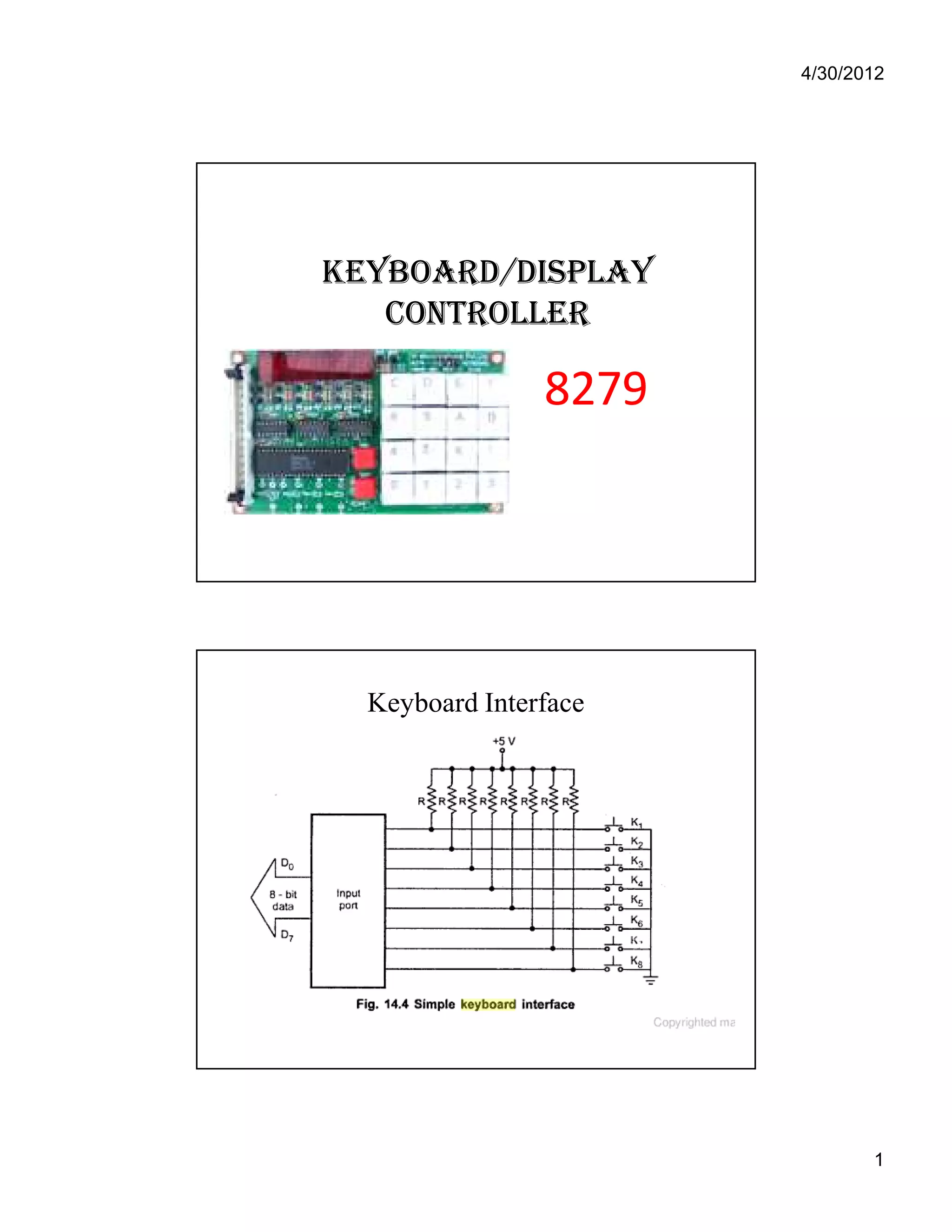
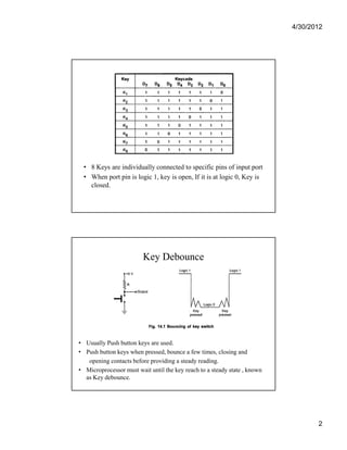
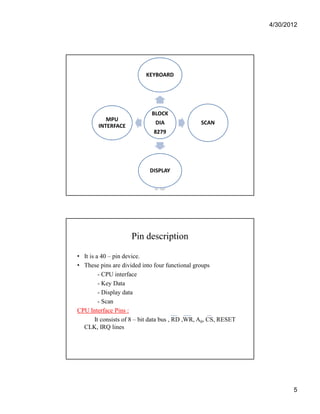
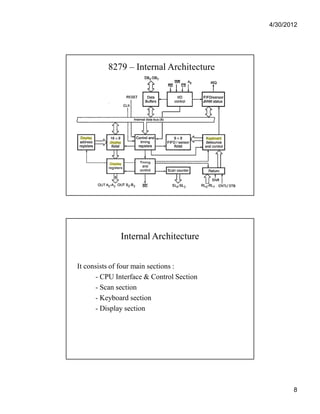
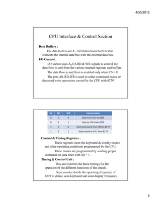
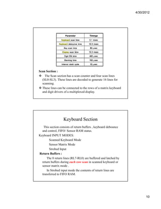
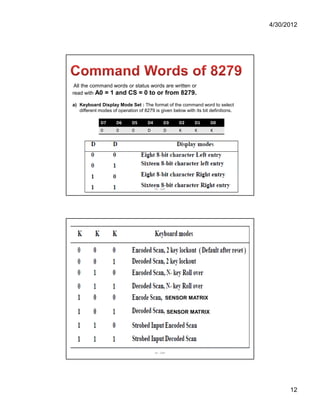
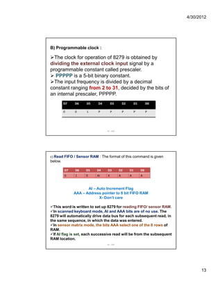
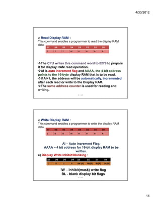
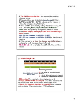
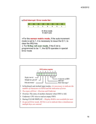
4/30/2012 
1 
KKEEYYBBOOAARRDD//DDIISSPPLLAAYY 
CCOONNTTRROOLLLLEERR 
88227799 
Keyboard Interface
4/30/2012 
2 
• 8 Keys are individually connected to specific pins of input port 
• When port pin is logic 1, key is open, If it is at logic 0, Key is 
closed. 
Key Debounce 
• Usually Push button keys are used. 
• Push button keys when pressed, bounce a few times, closing and 
opening contacts before providing a steady reading. 
• Microprocessor must wait until the key reach to a steady state , known 
as Key debounce.
4/30/2012 
3 
Introduction to 8279 
• Intel 8279 is a keyboard/display controller that simultaneously drives 
the display of a system and interfaces a keyboard with the CPU. 
• Keyboard display interface scans the keyboard to identify if any key is 
pressed and sends the code to the CPU and also transmits the data 
received from CPU to display device. 
• Keyboard can operate in two modes 
- Two Key lockout 
- N – Key rollover 
Two key lockout : 
If two keys are pressed almost simultaneously only the first key is 
recognized. 
N – Key rollover : 
Simultaneous Keys are recognised and their codes are stored in 
internal buffer, here no key will be recognised until only one key is 
pressed. 
Introduction to 8279….. 
• The Keyboard section can interface an array of a maximum of 64 
keys with the CPU. 
• The Key codes are stored in an 8-byte FIFO RAM that can be 
accessed by the CPU. If more than eight characters are entered in 
FIFO, overrun status is set. 
• Once the CPU reads a Key entry , the corresponding Key entry is 
pushed out of FIFO to generate space for new entries. 
• 8279 provides a maximum of sixteen 7 – segment display 
interface with CPU. 
• It contains a 16-byte display RAM that can be used either as an 
integrated block of 16x8 – bits or two 16x4 –bits of RAM.
4/30/2012 
4 
Keyboard 
segment 
• Connected to a 64 contact key matrix 
• Keyboard entries and debounced and 
stored in FIFO 
• Interrupt signal is generated with each 
entry 
Display 
segment 
• 16character scanned display 
• 16x8 R/W memory ( RAM ) 
• Right entry or left entry 
IIE - SAP
4/30/2012 
5 
KEYBOARD 
BLOCK 
DIA 
8279 
SCAN 
DISPLAY 
MPU 
INTERFACE 
IIE - SAP 
Pin description 
• It is a 40 – pin device. 
• These pins are divided into four functional groups 
- CPU interface 
- Key Data 
- Display data 
- Scan 
CPU Interface Pins : 
It consists of 8 – bit data bus , RD ,WR, A0, CS, RESET 
CLK, IRQ lines
4/30/2012 
6 
DB0 – DB7 : 
All data, Commands and status information between CPU 
and 8279 are transmitted on these bidirectional lines. 
RD : 
When this signal is low, CPU reads the contents of selected 
register (i.e) display RAM, status register, FIFO RAM. 
WR : 
When this signal is low, CPU loads the data into selected 
register (i.e) control register or display register. 
A0 : 
When A0 is high , signals are interpreted as command or 
status ; when A0 is low, signals are interpreted as data. 
CS : 
When the CS is active low ,it enables communication 
between CPU and 8279 
RESET : 
A HIGH on this pin resets 8279 and following modes are 
configured : 
1) Sixteen 8 – bit character display – left entry 
2) Encoded scan keyboard – 2 key lockout 
3) Program clock prescalar is set to 31. 
CLK : 
Is used to generate the internal timings required by 8279. 
IRQ : 
IRQ goes high whenever there is a data is to be read in FIFO 
RAM, IRQ goes low after each FIFO read operation.
4/30/2012 
7 
Keyboard Data : 
This contains return, SHIFT and CNTL/STB lines. 
RL0-RL7 : 
These input lines are used to interface keyboard. These 
lines keep their status HIGH. When the key from the keyboard 
is pressed corresponding return line goes low. 
SHIFT : 
It is a special key input line. Its status is stored along with 
the pressed key. The status of this key becomes low whenever 
a key is pressed. 
CNTL/STB : 
In Scanned Keyboard mode, this mode is used as control 
input. Similar to SHIFT key its status is also stored whenever a 
key is pressed. 
• In strobed input mode, this line is used as a strobed input , it 
loads the status of keyboard into FIFO RAM. 
Display Data : 
This group consists of OUT A3- A0, OUT B3-B0 & BD lines. 
OUT A3-A0 & B3 – B0 : 
Four bit output ports ,which can be considered as a single 8 – 
bit port. 
Used to send data to the display drivers from display RAM 
and connected to the 7 – segment (SL0-SL3) for multiplexed 
display. 
BD : 
This is an active low signal used to blank the display by 
displaying a blanking command.
4/30/2012 
8 
8279 – Internal Architecture 
Internal Architecture 
It consists of four main sections : 
- CPU Interface & Control Section 
- Scan section 
- Keyboard section 
- Display section
4/30/2012 
9 
CPU Interface & Control Section 
Data Buffers : 
The data buffers are 8 – bit bidirectional buffers that 
connects the internal data bus with the external data bus. 
I/O Control : 
I/O section uses A0,CS,RD & WR signals to control the 
data flow to and from the various internal registers and buffers. 
The data flow to and from is enabled only when CS = 0. 
The pins A0, RD,WR is used to select command ,status or 
data read/write operations carried by the CPU with 8279. 
A0 RD WR Interpretation 
0 1 0 Data from CPU to 8279 
0 0 1 Data to CPU from 8279 
1 1 0 Command word from CPU to 8279 
1 0 1 Status word to CPU from 8279 
Control & Timing Registers : 
These registers store the keyboard & display modes 
and other operating conditions programmed by the CPU. 
These modes are programmed by sending proper 
command on data lines with A0 = 1 . 
Timing & Control Unit : 
This unit controls the basic timings for the 
operation of the different functions of the circuit. 
Scan counter divide the operating frequency of 
8279 to derive scan keyboard and scan display frequency.
4/30/2012 
10 
Scan Section : 
 The Scan section has a scan counter and four scan lines 
(SL0-SL3). These lines are decoded to generate 16 lines for 
scanning. 
 These lines can be connected to the rows of a matrix keyboard 
and digit drivers of a multiplexed display. 
Keyboard Section 
This section consists of return buffers , keyboard debounce 
and control, FIFO/ Sensor RAM status. 
Keyboard INPUT MODES: 
Scanned Keyboard Mode 
Sensor Matrix Mode 
Strobed Input 
Return Buffers : 
The 8 return lines (RL7-RL0) are buffered and latched by 
return buffers during each row scan in scanned keyboard or 
sensor matrix mode . 
In Strobed input mode the contents of return lines are 
transferred to FIFO RAM.
4/30/2012 
11 
Keyboard Debounce  Control : 
This is enabled only when scanned keyboard mode is 
selected. In the scanned keyboard mode ,return lines are 
scanned , looking for a key closure in a row. 
If debounce circuit detects a close switch , it waits for 
10ms to check if the switch is closed. If a switch is identified , 
the address of the switch plus the status of the SHIFT  
CONTROL keys are transferred to FIFO RAM. 
FIFO/Sensor RAM : 
This is a dual function 8x8 RAM. In scanned keyboard and 
strobed input modes, it is a FIFO RAM. 
In Sensor Matrix mode, the memory is referred to as sensor 
RAM which is loaded with the status of the corresponding row 
of sensor in the sensor matrix. 
FIFO RAM STATUS : 
FIFO RAM keeps status of the number of characters in 
FIFO and whether it is full or empty. 
Display Section : 
The display section consists of display RAM, display address 
and display registers 
Display RAM : 
It is a 16x8 RAM which stores the display codes for 16 digits. 
Display address register : 
This register holds the address of the byte currently being 
written or read by the CPU and scan count value. 
Display registers: 
These registers hold the bit pattern of character to be 
displayed.
4/30/2012 
12 
All the command words or status words are written or 
read with A0 = 1 and CS = 0 to or from 8279. 
a) Keyboard Display Mode Set : The format of the command word to select 
different modes of operation of 8279 is given below with its bit definitions. 
D7 D6 D5 D4 D3 D2 D1 D0 
0 0 0 D D K K K 
IIE - SAP 
SENSOR MATRIX 
SENSOR MATRIX 
IIE - SAP
4/30/2012 
13 
B) Programmable clock : 
The clock for operation of 8279 is obtained by 
dividing the external clock input signal by a 
programmable constant called prescaler. 
 PPPPP is a 5-bit binary constant. 
The input frequency is divided by a decimal 
constant ranging from 2 to 31, decided by the bits of 
an internal prescaler, PPPPP. 
D7 D6 D5 D4 D3 D2 D1 D0 
0 0 1 P P P P P 
IIE - SAP 
c) Read FIFO / Sensor RAM : The format of this command is given 
below. 
D7 D6 D5 D4 D3 D2 D1 D0 
0 1 0 AI X A A A 
AI – Auto Increment Flag 
AAA – Address pointer to 8 bit FIFO RAM 
X- Don’t care 
This word is written to set up 8279 for reading FIFO/ sensor RAM. 
In scanned keyboard mode, AI and AAA bits are of no use. The 
8279 will automatically drive data bus for each subsequent read, in 
the same sequence, in which the data was entered. 
In sensor matrix mode, the bits AAA select one of the 8 rows of 
RAM. 
If AI flag is set, each successive read will be from the subsequent 
RAM location. 
IIE - SAP
4/30/2012 
14 
d) Read Display RAM : 
This command enables a programmer to read the display RAM 
data. 
D7 D6 D5 D4 D3 D2 D1 D0 
0 1 1 AI A A A A 
The CPU writes this command word to 8279 to prepare 
it for display RAM read operation. 
AI is auto increment flag and AAAA, the 4-bit address 
points to the 16-byte display RAM that is to be read. 
If AI=1, the address will be automatically, incremented 
after each read or write to the Display RAM. 
The same address counter is used for reading and 
writing. 
IIE - SAP 
d) Write Display RAM : 
This command enables a programmer to write the display RAM 
data. 
D7 D6 D5 D4 D3 D2 D1 D0 
1 0 0 AI A A A A 
AI – Auto increment Flag. 
AAAA – 4 bit address for 16-bit display RAM to be 
written. 
e) Display Write Inhibit/Blanking : 
D7 D6 D5 D4 D3 D2 D1 D0 
1 0 1 X IW (A) IW(B) BL(A) BL(B) 
IW – inhibit(mask) write flag 
BL - blank display bit flags 
IIE - SAP
4/30/2012 
15 
 The IW ( inhibit write flag ) bits are used to mask the 
individual nibble. 
The output lines are divided into two nibbles ( OUTA0 – 
OUTA3 ) and (OUTB0 – OUTB3 ), those can be masked by 
setting the corresponding IW bit to 1. 
 Once a nibble is masked by setting the corresponding IW 
bit to 1, the entry to display RAM does not affect the 
nibble even though it may change the unmasked nibble. 
The blank display bit flags (BL) are used for blanking A 
and B nibbles. 
D0, D2 corresponds to OUTB0 – OUTB3 
D1, D3 corresponds to OUTA0 - OUTA3 for blanking and 
masking. 
 If the user wants to clear the display, blank (BL) bits are 
available for each nibble as shown in format. 
Both BL bits will have to be cleared for blanking both the 
nibbles. 
IIE - SAP 
g) Clear Display RAM : 
D7 D6 D5 D4 D3 D2 D1 D0 
1 1 0 CD2 CD1 CD0 CF CA 
CD2 CD1 CD0 
ENABLES CLEAR DISPLAY 
WHEN CD2=1 
0X - All zeros ( for common cathode 
displays) 
10 - A3-A0 =2 (for alphanumeric displays) 
11 - All ones (for common anode displays) 
•CD2 must be 1 for enabling the clear display command. 
• If CF(CLEAR FIFO RAM STATUS) =1, FIFO status is cleared and 
IRQ line is pulled down and the sensor RAM address to 000. 
•If CA=1, this combines the effect of CD and CF bits ( clears the 
code on display RAM and also clears FIFO RAM status.
4/30/2012 
16 
h) End Interrupt / Error mode Set : 
D7 D6 D5 D4 D3 D2 D1 D0 
1 1 1 E X X X 1 
E- Error mode 
X- don’t care 
For the sensor matrix mode, if the auto-increment 
mode is set to 1, it is necessary to issue the E=1, to 
clear the IRQ line. 
 For N-Key roll over mode, if the E bit is 
programmed to be ‘1’, the 8279 operates in special 
Error mode 
FIFO status register 
• In Keyboard and strobed input modes, it is necessary to indicate the 
number of characters in FIFO and the indication of error. 
• Two types of Error : Overrun and Underrun 
• Overrun :The entry of another character when FIFO is full. 
• Underrun: CPU tries to read an empty FIFO. 
• During CLEAR DISPLAY – Display RAM is not available for user. 
• In special Error mode, S/E bit is set to indicate that a simultaneous 
multiple keys are entered.

8279 d

  • 1.
    4/30/2012 1 KKEEYYBBOOAARRDD//DDIISSPPLLAAYY CCOONNTTRROOLLLLEERR 88227799 Keyboard Interface
  • 2.
    4/30/2012 2 •8 Keys are individually connected to specific pins of input port • When port pin is logic 1, key is open, If it is at logic 0, Key is closed. Key Debounce • Usually Push button keys are used. • Push button keys when pressed, bounce a few times, closing and opening contacts before providing a steady reading. • Microprocessor must wait until the key reach to a steady state , known as Key debounce.
  • 3.
    4/30/2012 3 Introductionto 8279 • Intel 8279 is a keyboard/display controller that simultaneously drives the display of a system and interfaces a keyboard with the CPU. • Keyboard display interface scans the keyboard to identify if any key is pressed and sends the code to the CPU and also transmits the data received from CPU to display device. • Keyboard can operate in two modes - Two Key lockout - N – Key rollover Two key lockout : If two keys are pressed almost simultaneously only the first key is recognized. N – Key rollover : Simultaneous Keys are recognised and their codes are stored in internal buffer, here no key will be recognised until only one key is pressed. Introduction to 8279….. • The Keyboard section can interface an array of a maximum of 64 keys with the CPU. • The Key codes are stored in an 8-byte FIFO RAM that can be accessed by the CPU. If more than eight characters are entered in FIFO, overrun status is set. • Once the CPU reads a Key entry , the corresponding Key entry is pushed out of FIFO to generate space for new entries. • 8279 provides a maximum of sixteen 7 – segment display interface with CPU. • It contains a 16-byte display RAM that can be used either as an integrated block of 16x8 – bits or two 16x4 –bits of RAM.
  • 4.
    4/30/2012 4 Keyboard segment • Connected to a 64 contact key matrix • Keyboard entries and debounced and stored in FIFO • Interrupt signal is generated with each entry Display segment • 16character scanned display • 16x8 R/W memory ( RAM ) • Right entry or left entry IIE - SAP
  • 5.
    4/30/2012 5 KEYBOARD BLOCK DIA 8279 SCAN DISPLAY MPU INTERFACE IIE - SAP Pin description • It is a 40 – pin device. • These pins are divided into four functional groups - CPU interface - Key Data - Display data - Scan CPU Interface Pins : It consists of 8 – bit data bus , RD ,WR, A0, CS, RESET CLK, IRQ lines
  • 6.
    4/30/2012 6 DB0– DB7 : All data, Commands and status information between CPU and 8279 are transmitted on these bidirectional lines. RD : When this signal is low, CPU reads the contents of selected register (i.e) display RAM, status register, FIFO RAM. WR : When this signal is low, CPU loads the data into selected register (i.e) control register or display register. A0 : When A0 is high , signals are interpreted as command or status ; when A0 is low, signals are interpreted as data. CS : When the CS is active low ,it enables communication between CPU and 8279 RESET : A HIGH on this pin resets 8279 and following modes are configured : 1) Sixteen 8 – bit character display – left entry 2) Encoded scan keyboard – 2 key lockout 3) Program clock prescalar is set to 31. CLK : Is used to generate the internal timings required by 8279. IRQ : IRQ goes high whenever there is a data is to be read in FIFO RAM, IRQ goes low after each FIFO read operation.
  • 7.
    4/30/2012 7 KeyboardData : This contains return, SHIFT and CNTL/STB lines. RL0-RL7 : These input lines are used to interface keyboard. These lines keep their status HIGH. When the key from the keyboard is pressed corresponding return line goes low. SHIFT : It is a special key input line. Its status is stored along with the pressed key. The status of this key becomes low whenever a key is pressed. CNTL/STB : In Scanned Keyboard mode, this mode is used as control input. Similar to SHIFT key its status is also stored whenever a key is pressed. • In strobed input mode, this line is used as a strobed input , it loads the status of keyboard into FIFO RAM. Display Data : This group consists of OUT A3- A0, OUT B3-B0 & BD lines. OUT A3-A0 & B3 – B0 : Four bit output ports ,which can be considered as a single 8 – bit port. Used to send data to the display drivers from display RAM and connected to the 7 – segment (SL0-SL3) for multiplexed display. BD : This is an active low signal used to blank the display by displaying a blanking command.
  • 8.
    4/30/2012 8 8279– Internal Architecture Internal Architecture It consists of four main sections : - CPU Interface & Control Section - Scan section - Keyboard section - Display section
  • 9.
    4/30/2012 9 CPUInterface & Control Section Data Buffers : The data buffers are 8 – bit bidirectional buffers that connects the internal data bus with the external data bus. I/O Control : I/O section uses A0,CS,RD & WR signals to control the data flow to and from the various internal registers and buffers. The data flow to and from is enabled only when CS = 0. The pins A0, RD,WR is used to select command ,status or data read/write operations carried by the CPU with 8279. A0 RD WR Interpretation 0 1 0 Data from CPU to 8279 0 0 1 Data to CPU from 8279 1 1 0 Command word from CPU to 8279 1 0 1 Status word to CPU from 8279 Control & Timing Registers : These registers store the keyboard & display modes and other operating conditions programmed by the CPU. These modes are programmed by sending proper command on data lines with A0 = 1 . Timing & Control Unit : This unit controls the basic timings for the operation of the different functions of the circuit. Scan counter divide the operating frequency of 8279 to derive scan keyboard and scan display frequency.
  • 10.
    4/30/2012 10 ScanSection : The Scan section has a scan counter and four scan lines (SL0-SL3). These lines are decoded to generate 16 lines for scanning. These lines can be connected to the rows of a matrix keyboard and digit drivers of a multiplexed display. Keyboard Section This section consists of return buffers , keyboard debounce and control, FIFO/ Sensor RAM status. Keyboard INPUT MODES: Scanned Keyboard Mode Sensor Matrix Mode Strobed Input Return Buffers : The 8 return lines (RL7-RL0) are buffered and latched by return buffers during each row scan in scanned keyboard or sensor matrix mode . In Strobed input mode the contents of return lines are transferred to FIFO RAM.
  • 11.
    4/30/2012 11 KeyboardDebounce Control : This is enabled only when scanned keyboard mode is selected. In the scanned keyboard mode ,return lines are scanned , looking for a key closure in a row. If debounce circuit detects a close switch , it waits for 10ms to check if the switch is closed. If a switch is identified , the address of the switch plus the status of the SHIFT CONTROL keys are transferred to FIFO RAM. FIFO/Sensor RAM : This is a dual function 8x8 RAM. In scanned keyboard and strobed input modes, it is a FIFO RAM. In Sensor Matrix mode, the memory is referred to as sensor RAM which is loaded with the status of the corresponding row of sensor in the sensor matrix. FIFO RAM STATUS : FIFO RAM keeps status of the number of characters in FIFO and whether it is full or empty. Display Section : The display section consists of display RAM, display address and display registers Display RAM : It is a 16x8 RAM which stores the display codes for 16 digits. Display address register : This register holds the address of the byte currently being written or read by the CPU and scan count value. Display registers: These registers hold the bit pattern of character to be displayed.
  • 12.
    4/30/2012 12 Allthe command words or status words are written or read with A0 = 1 and CS = 0 to or from 8279. a) Keyboard Display Mode Set : The format of the command word to select different modes of operation of 8279 is given below with its bit definitions. D7 D6 D5 D4 D3 D2 D1 D0 0 0 0 D D K K K IIE - SAP SENSOR MATRIX SENSOR MATRIX IIE - SAP
  • 13.
    4/30/2012 13 B)Programmable clock : The clock for operation of 8279 is obtained by dividing the external clock input signal by a programmable constant called prescaler. PPPPP is a 5-bit binary constant. The input frequency is divided by a decimal constant ranging from 2 to 31, decided by the bits of an internal prescaler, PPPPP. D7 D6 D5 D4 D3 D2 D1 D0 0 0 1 P P P P P IIE - SAP c) Read FIFO / Sensor RAM : The format of this command is given below. D7 D6 D5 D4 D3 D2 D1 D0 0 1 0 AI X A A A AI – Auto Increment Flag AAA – Address pointer to 8 bit FIFO RAM X- Don’t care This word is written to set up 8279 for reading FIFO/ sensor RAM. In scanned keyboard mode, AI and AAA bits are of no use. The 8279 will automatically drive data bus for each subsequent read, in the same sequence, in which the data was entered. In sensor matrix mode, the bits AAA select one of the 8 rows of RAM. If AI flag is set, each successive read will be from the subsequent RAM location. IIE - SAP
  • 14.
    4/30/2012 14 d)Read Display RAM : This command enables a programmer to read the display RAM data. D7 D6 D5 D4 D3 D2 D1 D0 0 1 1 AI A A A A The CPU writes this command word to 8279 to prepare it for display RAM read operation. AI is auto increment flag and AAAA, the 4-bit address points to the 16-byte display RAM that is to be read. If AI=1, the address will be automatically, incremented after each read or write to the Display RAM. The same address counter is used for reading and writing. IIE - SAP d) Write Display RAM : This command enables a programmer to write the display RAM data. D7 D6 D5 D4 D3 D2 D1 D0 1 0 0 AI A A A A AI – Auto increment Flag. AAAA – 4 bit address for 16-bit display RAM to be written. e) Display Write Inhibit/Blanking : D7 D6 D5 D4 D3 D2 D1 D0 1 0 1 X IW (A) IW(B) BL(A) BL(B) IW – inhibit(mask) write flag BL - blank display bit flags IIE - SAP
  • 15.
    4/30/2012 15 The IW ( inhibit write flag ) bits are used to mask the individual nibble. The output lines are divided into two nibbles ( OUTA0 – OUTA3 ) and (OUTB0 – OUTB3 ), those can be masked by setting the corresponding IW bit to 1. Once a nibble is masked by setting the corresponding IW bit to 1, the entry to display RAM does not affect the nibble even though it may change the unmasked nibble. The blank display bit flags (BL) are used for blanking A and B nibbles. D0, D2 corresponds to OUTB0 – OUTB3 D1, D3 corresponds to OUTA0 - OUTA3 for blanking and masking. If the user wants to clear the display, blank (BL) bits are available for each nibble as shown in format. Both BL bits will have to be cleared for blanking both the nibbles. IIE - SAP g) Clear Display RAM : D7 D6 D5 D4 D3 D2 D1 D0 1 1 0 CD2 CD1 CD0 CF CA CD2 CD1 CD0 ENABLES CLEAR DISPLAY WHEN CD2=1 0X - All zeros ( for common cathode displays) 10 - A3-A0 =2 (for alphanumeric displays) 11 - All ones (for common anode displays) •CD2 must be 1 for enabling the clear display command. • If CF(CLEAR FIFO RAM STATUS) =1, FIFO status is cleared and IRQ line is pulled down and the sensor RAM address to 000. •If CA=1, this combines the effect of CD and CF bits ( clears the code on display RAM and also clears FIFO RAM status.
  • 16.
    4/30/2012 16 h)End Interrupt / Error mode Set : D7 D6 D5 D4 D3 D2 D1 D0 1 1 1 E X X X 1 E- Error mode X- don’t care For the sensor matrix mode, if the auto-increment mode is set to 1, it is necessary to issue the E=1, to clear the IRQ line. For N-Key roll over mode, if the E bit is programmed to be ‘1’, the 8279 operates in special Error mode FIFO status register • In Keyboard and strobed input modes, it is necessary to indicate the number of characters in FIFO and the indication of error. • Two types of Error : Overrun and Underrun • Overrun :The entry of another character when FIFO is full. • Underrun: CPU tries to read an empty FIFO. • During CLEAR DISPLAY – Display RAM is not available for user. • In special Error mode, S/E bit is set to indicate that a simultaneous multiple keys are entered.