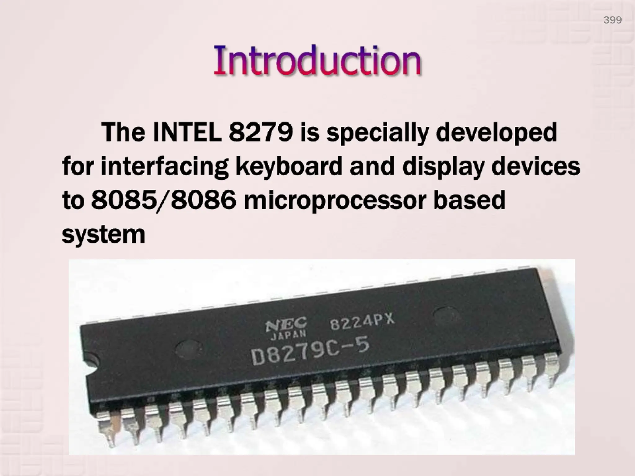
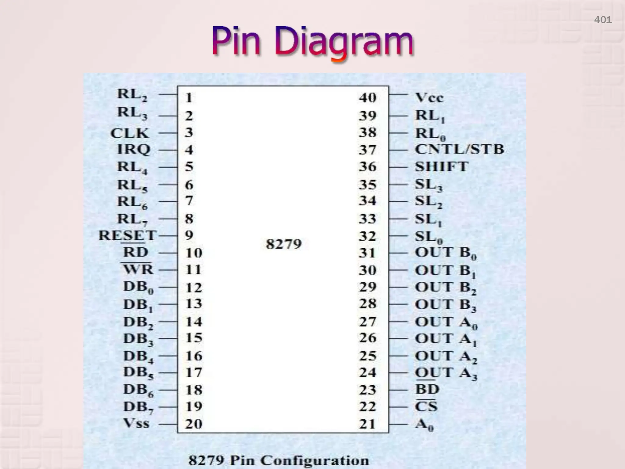
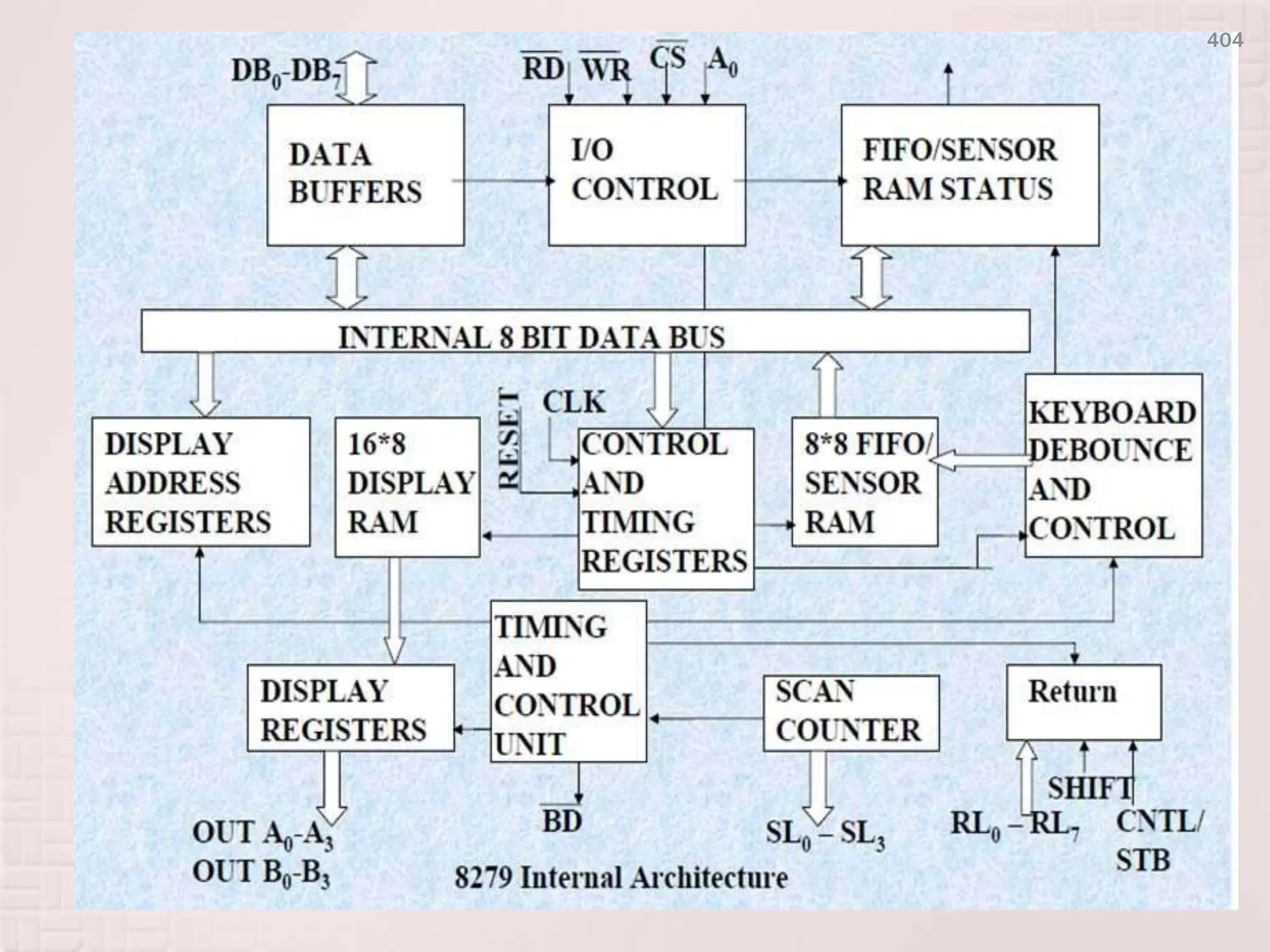
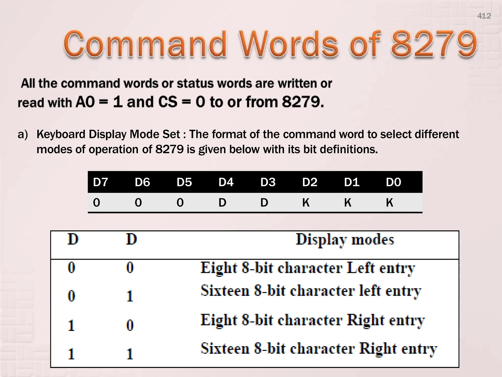
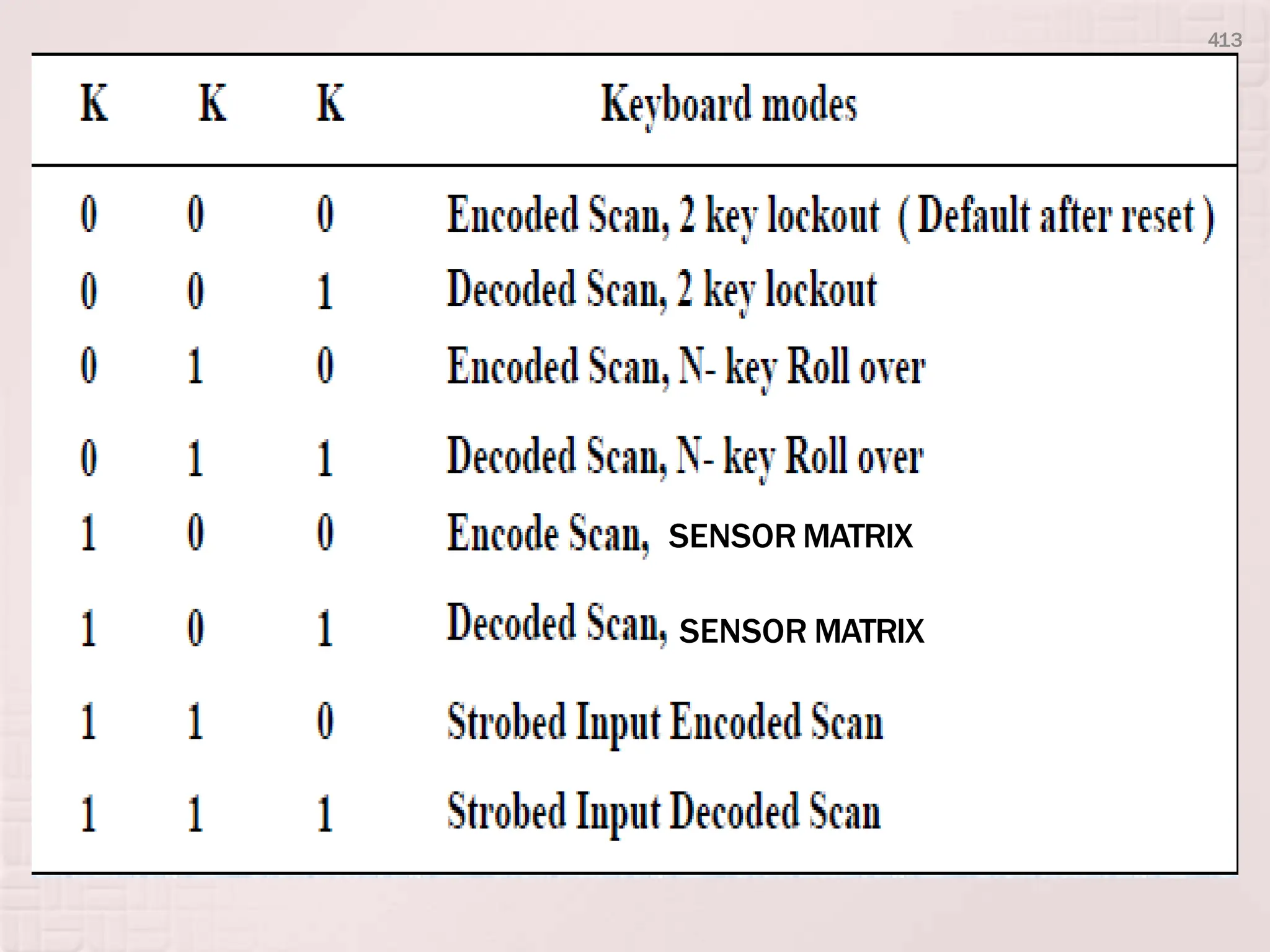
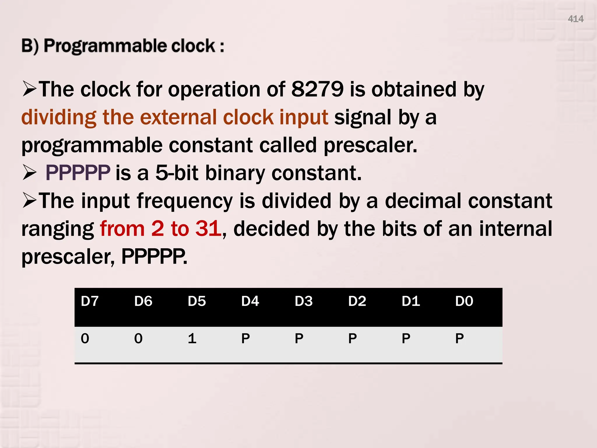
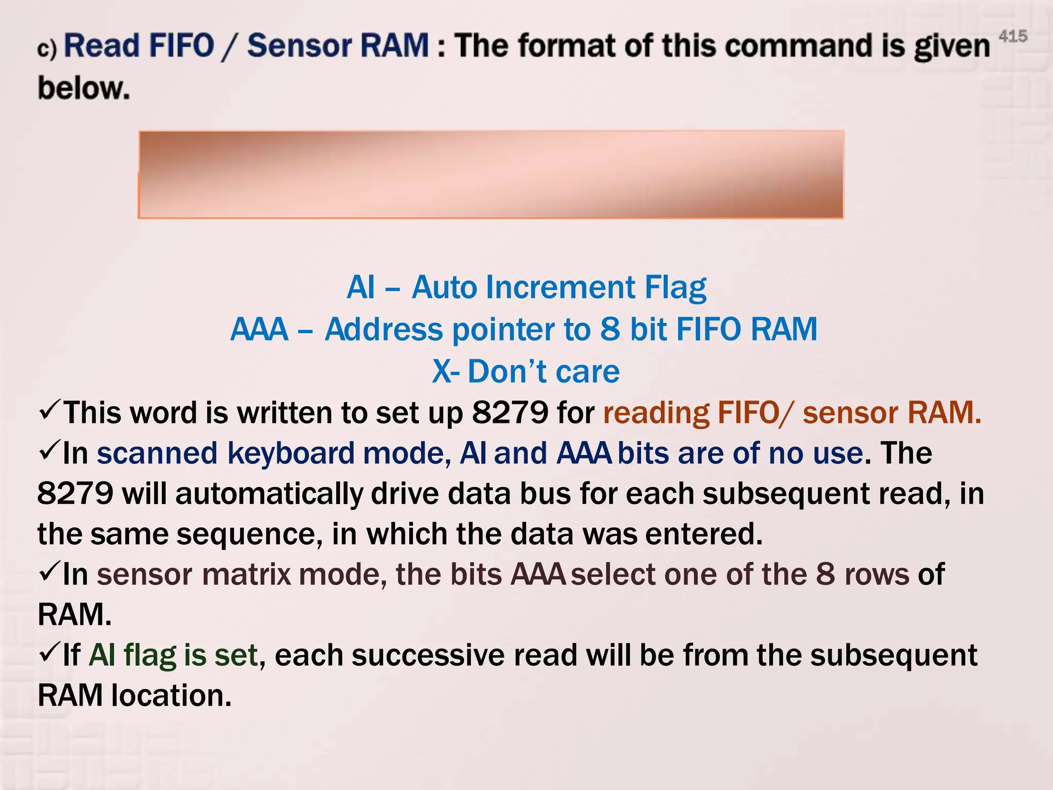
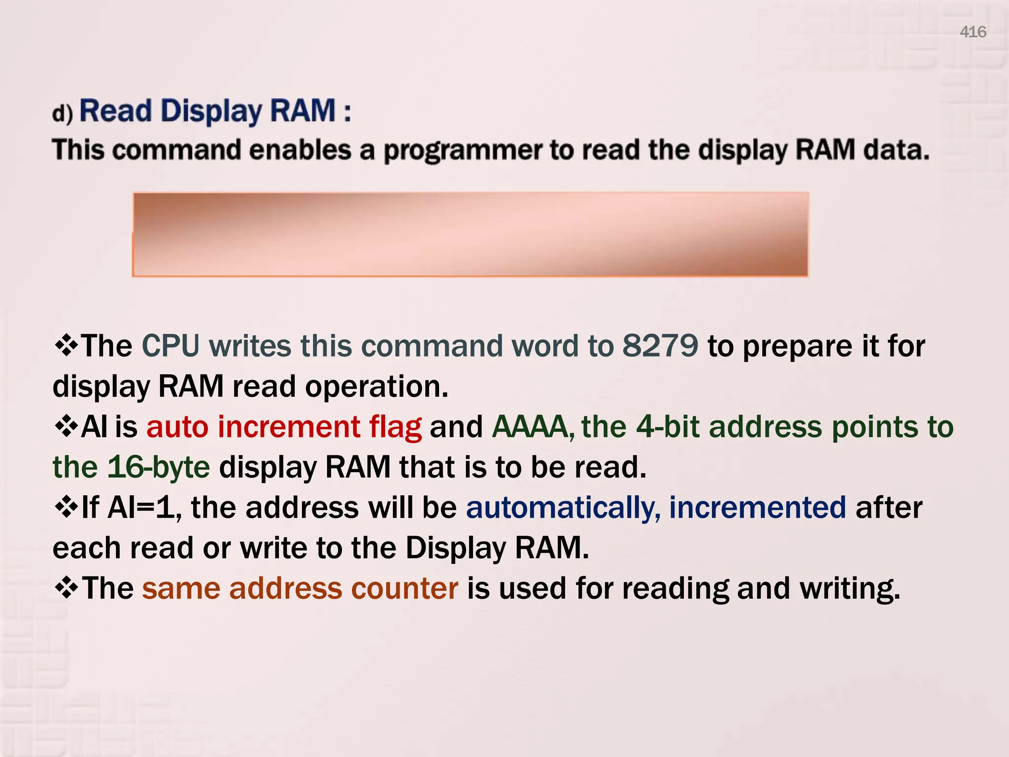
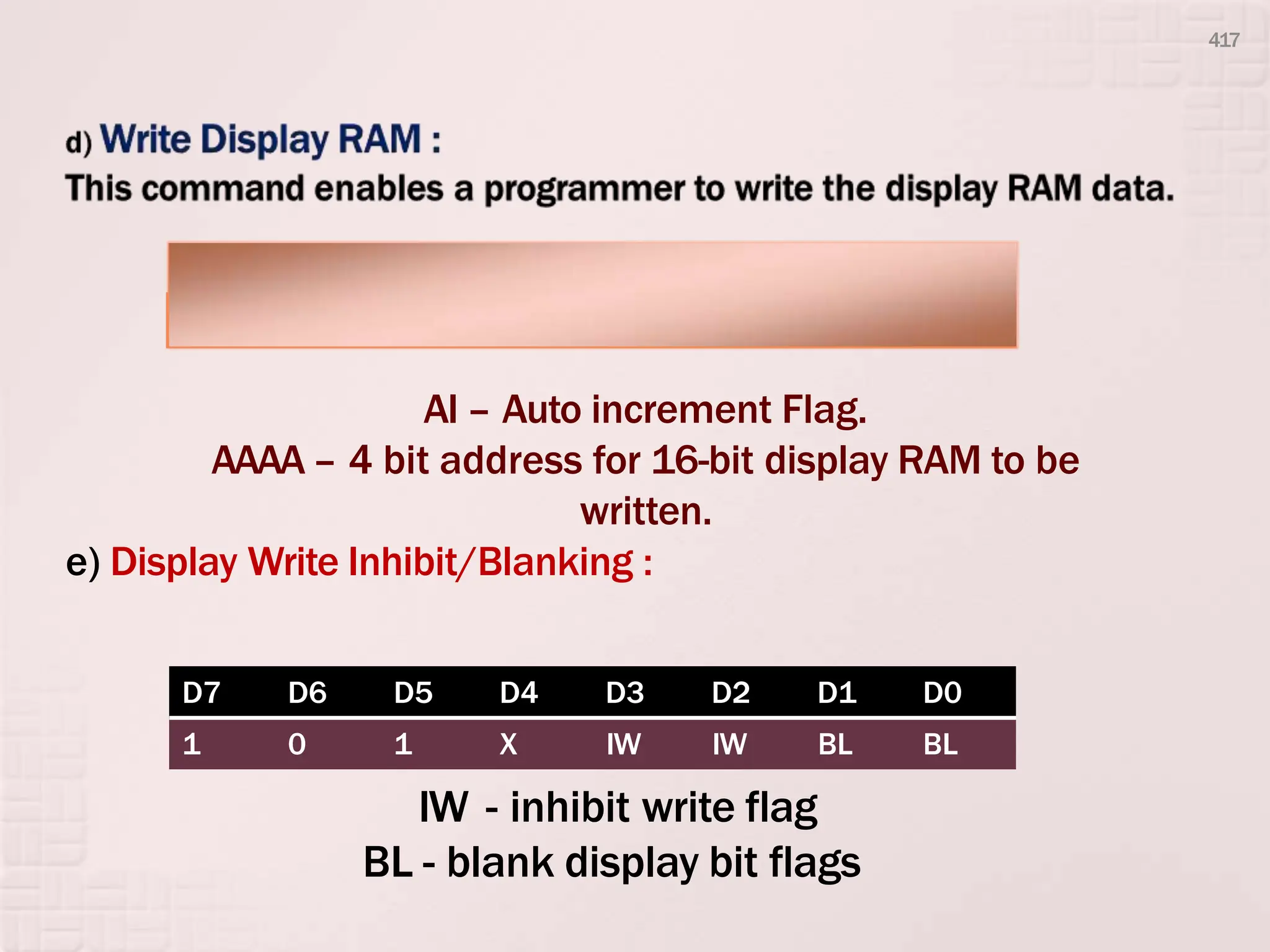
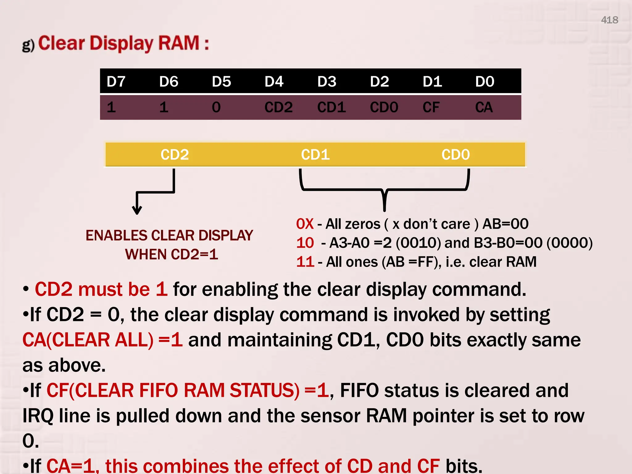
KEYBOARD/DISPLAY
CONTROLLER INTEL 8279
398
399
 Scanned sensor mode
 8-character keyboard FIFO
 1 6-character display
400
401
 Display section
 Scan section
 CPU interface section
402
403
404
 The keyboard section consists of 8 return
lines RL0 - RL7 that can be used to form the
columns of a keyboard matrix.
 It has two additional input : shift and
control/strobe. The keys are automatically
debounced.
 The two operating modes of keyboard
section are 2-key lockout and N-key rollover.
405
 The keyboard section also have an 8 x 8
FIFO (First In First Out) RAM.
 The FIFO can store eight key codes in the scan
keyboard mode. The status of the shift key and
control key are also stored along with key code. The
8279 generate an interrupt signal (IRQ)when there
is an entry in FIFO.
406
 The display section has eight output lines
divided into two groups A0-A3 and B0-B3.
 The output lines can be used either as a
single group of eight lines or as two groups
of four lines, in conjunction with the scan
lines for a multiplexed display.
 The output lines are connected to the
anodes through driver transistor in case of
common cathode 7-segment LEDs.
407
 The display can be blanked by BD (low) line.
 The display section consists of 16 x 8 display
RAM. The CPU can read from or write into
any location of the display RAM.
408
 In decoded scan mode, the output of scan lines will
be similar to a 2-to-4 decoder.
 In encoded scan mode, the output of scan lines
will be binary count, and so an external decoder
should be used to convert the binary count to
decoded output.
 The scan lines are common for keyboard and
display.
409
 The CPU interface section takes care of data
transfer between 8279 and the processor.
 This section has eight bidirectional data
lines DB0 to DB7 for data transfer between
8279 and CPU.
 It requires two internal address A=0 for
selecting data buffer and A = 1 for selecting
control register of8279.
410
 The 8279 require an internal clock
frequency of 100 kHz. This can be obtained
by dividing the input clock by an internal
prescaler.
411
a) Keyboard Display Mode Set : The format of the command word to select different
modes of operation of 8279 is given below with its bit definitions.
D7 D6 D5 D4 D3 D2 D1 D0
0 0 0 D D K K K
412
SENSOR MATRIX
SENSOR MATRIX
413
The clock for operation of 8279 is obtained by
dividing the external clock input signal by a
programmable constant called prescaler.
 PPPPP is a 5-bit binary constant.
The input frequency is divided by a decimal constant
ranging from 2 to 31, decided by the bits of an internal
prescaler, PPPPP.
D7 D6 D5 D4 D3 D2 D1 D0
0 0 1 P P P P P
414
AI – Auto Increment Flag
AAA – Address pointer to 8 bit FIFO RAM
X- Don’t care
This word is written to set up 8279 for reading FIFO/ sensor RAM.
In scanned keyboard mode, AI and AAAbits are of no use. The
8279 will automatically drive data bus for each subsequent read, in
the same sequence, in which the data was entered.
In sensor matrix mode, the bits AAAselect one of the 8 rows of
RAM.
If AI flag is set, each successive read will be from the subsequent
RAM location.
D7 D6 D5 D4 D3 D2 D1 D0
0 1 0 AI X A A A
The CPU writes this command word to 8279 to prepare it for
display RAM read operation.
AI is auto increment flag and AAAA,the 4-bit address points to
the 16-byte display RAM that is to be read.
If AI=1, the address will be automatically, incremented after
each read or write to the Display RAM.
The same address counter is used for reading and writing.
D7 D6 D5 D4 D3 D2 D1 D0
0 1 1 AI A A A A
416
AI – Auto increment Flag.
AAAA – 4 bit address for 16-bit display RAM to be
written.
e) Display Write Inhibit/Blanking :
D7 D6 D5 D4 D3 D2 D1 D0
1 0 0 AI A A A A
D7 D6 D5 D4 D3 D2 D1 D0
1 0 1 X IW IW BL BL
IW - inhibit write flag
BL - blank display bit flags
417
ENABLES CLEAR DISPLAY
WHEN CD2=1
• CD2 must be 1 for enabling the clear display command.
•If CD2 = 0, the clear display command is invoked by setting
CA(CLEAR ALL) =1 and maintaining CD1, CD0 bits exactly same
as above.
•If CF(CLEAR FIFO RAM STATUS) =1, FIFO status is cleared and
IRQ line is pulled down and the sensor RAM pointer is set to row
0.
•If CA=1, this combines the effect of CD and CF bits.
D7 D6 D5 D4 D3 D2 D1 D0
1 1 0 CD2 CD1 CD0 CF CA
CD2 CD1 CD0
0X - All zeros ( x don’t care ) AB=00
10 - A3-A0 =2 (0010) and B3-B0=00 (0000)
11 - All ones (AB =FF), i.e. clear RAM
418
E- Error mode
X- don’t care
For the sensor matrix mode, this command lowers the
IRQ line and enables further writing into the RAM.
Otherwise, if a change in sensor value is detected, IRQ
goes high that inhibits writing in the sensor RAM.
For N-Key roll over mode, if the E bit is programmed to
be ‘1’, the 8279 operates in special Error mode
D7 D6 D5 D4 D3 D2 D1 D0
1 1 1 E X X X 1
419

KEYBOARD/DISPLAY CONTROLLER INTEL 8279.pptx

  • 1.
  • 2.
  • 3.
  • 4.
     Scanned sensormode  8-character keyboard FIFO  1 6-character display 400
  • 5.
  • 6.
     Display section Scan section  CPU interface section 402
  • 7.
  • 8.
  • 9.
     The keyboardsection consists of 8 return lines RL0 - RL7 that can be used to form the columns of a keyboard matrix.  It has two additional input : shift and control/strobe. The keys are automatically debounced.  The two operating modes of keyboard section are 2-key lockout and N-key rollover. 405
  • 10.
     The keyboardsection also have an 8 x 8 FIFO (First In First Out) RAM.  The FIFO can store eight key codes in the scan keyboard mode. The status of the shift key and control key are also stored along with key code. The 8279 generate an interrupt signal (IRQ)when there is an entry in FIFO. 406
  • 11.
     The displaysection has eight output lines divided into two groups A0-A3 and B0-B3.  The output lines can be used either as a single group of eight lines or as two groups of four lines, in conjunction with the scan lines for a multiplexed display.  The output lines are connected to the anodes through driver transistor in case of common cathode 7-segment LEDs. 407
  • 12.
     The displaycan be blanked by BD (low) line.  The display section consists of 16 x 8 display RAM. The CPU can read from or write into any location of the display RAM. 408
  • 13.
     In decodedscan mode, the output of scan lines will be similar to a 2-to-4 decoder.  In encoded scan mode, the output of scan lines will be binary count, and so an external decoder should be used to convert the binary count to decoded output.  The scan lines are common for keyboard and display. 409
  • 14.
     The CPUinterface section takes care of data transfer between 8279 and the processor.  This section has eight bidirectional data lines DB0 to DB7 for data transfer between 8279 and CPU.  It requires two internal address A=0 for selecting data buffer and A = 1 for selecting control register of8279. 410
  • 15.
     The 8279require an internal clock frequency of 100 kHz. This can be obtained by dividing the input clock by an internal prescaler. 411
  • 16.
    a) Keyboard DisplayMode Set : The format of the command word to select different modes of operation of 8279 is given below with its bit definitions. D7 D6 D5 D4 D3 D2 D1 D0 0 0 0 D D K K K 412
  • 17.
  • 18.
    The clock foroperation of 8279 is obtained by dividing the external clock input signal by a programmable constant called prescaler.  PPPPP is a 5-bit binary constant. The input frequency is divided by a decimal constant ranging from 2 to 31, decided by the bits of an internal prescaler, PPPPP. D7 D6 D5 D4 D3 D2 D1 D0 0 0 1 P P P P P 414
  • 19.
    AI – AutoIncrement Flag AAA – Address pointer to 8 bit FIFO RAM X- Don’t care This word is written to set up 8279 for reading FIFO/ sensor RAM. In scanned keyboard mode, AI and AAAbits are of no use. The 8279 will automatically drive data bus for each subsequent read, in the same sequence, in which the data was entered. In sensor matrix mode, the bits AAAselect one of the 8 rows of RAM. If AI flag is set, each successive read will be from the subsequent RAM location. D7 D6 D5 D4 D3 D2 D1 D0 0 1 0 AI X A A A
  • 20.
    The CPU writesthis command word to 8279 to prepare it for display RAM read operation. AI is auto increment flag and AAAA,the 4-bit address points to the 16-byte display RAM that is to be read. If AI=1, the address will be automatically, incremented after each read or write to the Display RAM. The same address counter is used for reading and writing. D7 D6 D5 D4 D3 D2 D1 D0 0 1 1 AI A A A A 416
  • 21.
    AI – Autoincrement Flag. AAAA – 4 bit address for 16-bit display RAM to be written. e) Display Write Inhibit/Blanking : D7 D6 D5 D4 D3 D2 D1 D0 1 0 0 AI A A A A D7 D6 D5 D4 D3 D2 D1 D0 1 0 1 X IW IW BL BL IW - inhibit write flag BL - blank display bit flags 417
  • 22.
    ENABLES CLEAR DISPLAY WHENCD2=1 • CD2 must be 1 for enabling the clear display command. •If CD2 = 0, the clear display command is invoked by setting CA(CLEAR ALL) =1 and maintaining CD1, CD0 bits exactly same as above. •If CF(CLEAR FIFO RAM STATUS) =1, FIFO status is cleared and IRQ line is pulled down and the sensor RAM pointer is set to row 0. •If CA=1, this combines the effect of CD and CF bits. D7 D6 D5 D4 D3 D2 D1 D0 1 1 0 CD2 CD1 CD0 CF CA CD2 CD1 CD0 0X - All zeros ( x don’t care ) AB=00 10 - A3-A0 =2 (0010) and B3-B0=00 (0000) 11 - All ones (AB =FF), i.e. clear RAM 418
  • 23.
    E- Error mode X-don’t care For the sensor matrix mode, this command lowers the IRQ line and enables further writing into the RAM. Otherwise, if a change in sensor value is detected, IRQ goes high that inhibits writing in the sensor RAM. For N-Key roll over mode, if the E bit is programmed to be ‘1’, the 8279 operates in special Error mode D7 D6 D5 D4 D3 D2 D1 D0 1 1 1 E X X X 1 419