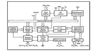
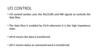
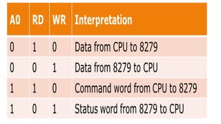
8279
KEYBOARD AND DISPLAY
INTERFACING
8279
• Intel’s 8279 is a general purpose Keyboard Display controller that
simultaneously drives the display of a system and interfaces a
Keyboard with the CPU.
• The Keyboard Display interface scans the Keyboard to identify if any
key has been pressed and sends the code of the pressed key to the
CPU.
• It also transmits the data received from the CPU, to the display
device.
• It is support 64 contact key matrix with two more keys “CONTROL”
and “SHIFT”
• It has inbuilt debounce key
• Two approaches to interface a matrix keyboard and a multiplexed
display to the microprocessor namely, 1) Hardware Approach 2)
Software Approach
• The disadvantage of software approach is that the microprocessor is
occupied for a considerable amount of time in checking the keyboard
and refreshing the display.
• Intel 8279 follows hardware approach and it has the advantage of
relieving the processor from the above mentioned two tasks. But it is
expensive.
• It provides 16 byte display RAM to display 16 digits and interfacing 16
digits.
• It provides two output modes:
1.Left entry (Typewriter type).
2.Right entry (Calculator type).
• It provides 8 byte FIFO RAM to store keywords.
• The interrupt output of 8279 can be used to tell CPU that the key
press is detected, this eliminates the need of software polling
• It is fully programmable, providing three modes of operation.The
three modes of operation are Scanned Keyboard mode, Scanned
Sensor Matrix mode, Strobed Input mode.
DATA BUFFERS
• 8-bit bidirectional buffer.
• Used to connect the internal data bus and external data bus.
• These lines are used for communication(i.e) transfer of data,
commands and status between the microprocessor(CPU) and 8279.
I/O CONTROL
• I/O control section uses the A0,CS,RD and WR signals to controls the
data flow.
• The data flow is enabled by CS=0 otherwise it is the high impedance
state.
• A0=0 means the data is transferred.
• A0=1 means status or command word is transferred.
TIMING AND CONTROL REGISTERS
• The control and timing registers store the keyboard and display
modes and other operating conditions programmed by the CPU
• The modes are programmed by sending the proper command on the
data lines with A0 = 1.
• The command is then decoded and the appropriate mode/function is
set.
TIMING AND CONTROL
It consist timing counter chain.
First counter is divided by N prescalar that can be programmed to
give an internal frequency of 100 KHz
The internal frequency of 100 KHz gives the internal timings
SCAN SECTION
It has two modes,
1) Encoded mode
2) Decoded mode.
• These lines can be decoded by a 4 to 16 decoder to generate 16 lines for
scanning
• In the encoded mode, the scan counter provides a binary count from
0000 to 1111 on the four scan lines (SC3 — SC0) with active high
outputs. This binary count must be externally decoded to provide 16
scan lines.
• Display can use all 16 scan lines to interface 16 digit 7-segment display,
but keyboard can use only 8 scan lines out of 16 scan lines.
• In the decoded mode, the internal decoder decodes the least
significant 2 bits of binary count and provides four possible
combinations on the scan lines (SC3 — SC0) :1110, 1101, 1011 and
0111.
• Thus the output of decoded scan is active low. These four active low
output lines can be used directly to interface 4 digit 7 segment
display, 8 x 4 matrix keyboard, eliminating the external decoder.
Keyboard section
This is consist of,
1) Return buffers.
2) Keyboard debounce control.
3) FIFO / sensor RAM.
4) FIFO / sensor RAM status
Return buffers has 8 return lines (RL0 — RL7) and two additional
lines: Shift and CNTL/STB (control/strobe).
In strobed mode ,the contents of return lines are transferred to FIFO
Ram
These lines are used to get the 8 column outputs from the keyboard
to 8279.
• The return lines are scanned whether the key is closed in the row or
not.
• If debounce circuit is detect any closed switch it wait about 10 msec.
• It is continued , the status of SHIFT and CONTROL keys are transferred
into RAM
FIFO/SENSOR RAM
• It is a dual function 8*8 RAM
• Each new entry is written into successive RAM position and read in the order of
entry
• Each row of the sensor RAM is loaded with the status of the corresponding row
of sensor in the sensor matrix.
FIFO/SENSOR RAM STATUS
 This is used to tell the status of FIFO/SENSOR RAM.
 The status of logic also makes IRQ signal is High , when the FIFO is not empty,
which can be used to interrupt CPU telling that key press is detected and
keycode is available in FIFO RAM.
DISPLAY SECTION
Used to hold address of the byte currently write or read by the CPU
and scan count value.
In auto increment mode, address in the register is automatically
incremented for each write or read
It is active low output signal and is used to blank the display during
digit switching or by a display blanking command.

MICROCONTROLLER 8279 KEYBOARD INTERFACE.pptx

  • 1.
  • 2.
    8279 • Intel’s 8279is a general purpose Keyboard Display controller that simultaneously drives the display of a system and interfaces a Keyboard with the CPU. • The Keyboard Display interface scans the Keyboard to identify if any key has been pressed and sends the code of the pressed key to the CPU. • It also transmits the data received from the CPU, to the display device. • It is support 64 contact key matrix with two more keys “CONTROL” and “SHIFT” • It has inbuilt debounce key
  • 3.
    • Two approachesto interface a matrix keyboard and a multiplexed display to the microprocessor namely, 1) Hardware Approach 2) Software Approach • The disadvantage of software approach is that the microprocessor is occupied for a considerable amount of time in checking the keyboard and refreshing the display. • Intel 8279 follows hardware approach and it has the advantage of relieving the processor from the above mentioned two tasks. But it is expensive.
  • 4.
    • It provides16 byte display RAM to display 16 digits and interfacing 16 digits. • It provides two output modes: 1.Left entry (Typewriter type). 2.Right entry (Calculator type). • It provides 8 byte FIFO RAM to store keywords. • The interrupt output of 8279 can be used to tell CPU that the key press is detected, this eliminates the need of software polling • It is fully programmable, providing three modes of operation.The three modes of operation are Scanned Keyboard mode, Scanned Sensor Matrix mode, Strobed Input mode.
  • 6.
    DATA BUFFERS • 8-bitbidirectional buffer. • Used to connect the internal data bus and external data bus. • These lines are used for communication(i.e) transfer of data, commands and status between the microprocessor(CPU) and 8279.
  • 7.
    I/O CONTROL • I/Ocontrol section uses the A0,CS,RD and WR signals to controls the data flow. • The data flow is enabled by CS=0 otherwise it is the high impedance state. • A0=0 means the data is transferred. • A0=1 means status or command word is transferred.
  • 9.
    TIMING AND CONTROLREGISTERS • The control and timing registers store the keyboard and display modes and other operating conditions programmed by the CPU • The modes are programmed by sending the proper command on the data lines with A0 = 1. • The command is then decoded and the appropriate mode/function is set. TIMING AND CONTROL It consist timing counter chain. First counter is divided by N prescalar that can be programmed to give an internal frequency of 100 KHz The internal frequency of 100 KHz gives the internal timings
  • 10.
    SCAN SECTION It hastwo modes, 1) Encoded mode 2) Decoded mode. • These lines can be decoded by a 4 to 16 decoder to generate 16 lines for scanning • In the encoded mode, the scan counter provides a binary count from 0000 to 1111 on the four scan lines (SC3 — SC0) with active high outputs. This binary count must be externally decoded to provide 16 scan lines. • Display can use all 16 scan lines to interface 16 digit 7-segment display, but keyboard can use only 8 scan lines out of 16 scan lines.
  • 11.
    • In thedecoded mode, the internal decoder decodes the least significant 2 bits of binary count and provides four possible combinations on the scan lines (SC3 — SC0) :1110, 1101, 1011 and 0111. • Thus the output of decoded scan is active low. These four active low output lines can be used directly to interface 4 digit 7 segment display, 8 x 4 matrix keyboard, eliminating the external decoder.
  • 12.
    Keyboard section This isconsist of, 1) Return buffers. 2) Keyboard debounce control. 3) FIFO / sensor RAM. 4) FIFO / sensor RAM status Return buffers has 8 return lines (RL0 — RL7) and two additional lines: Shift and CNTL/STB (control/strobe). In strobed mode ,the contents of return lines are transferred to FIFO Ram These lines are used to get the 8 column outputs from the keyboard to 8279.
  • 13.
    • The returnlines are scanned whether the key is closed in the row or not. • If debounce circuit is detect any closed switch it wait about 10 msec. • It is continued , the status of SHIFT and CONTROL keys are transferred into RAM
  • 14.
    FIFO/SENSOR RAM • Itis a dual function 8*8 RAM • Each new entry is written into successive RAM position and read in the order of entry • Each row of the sensor RAM is loaded with the status of the corresponding row of sensor in the sensor matrix. FIFO/SENSOR RAM STATUS  This is used to tell the status of FIFO/SENSOR RAM.  The status of logic also makes IRQ signal is High , when the FIFO is not empty, which can be used to interrupt CPU telling that key press is detected and keycode is available in FIFO RAM.
  • 15.
    DISPLAY SECTION Used tohold address of the byte currently write or read by the CPU and scan count value. In auto increment mode, address in the register is automatically incremented for each write or read It is active low output signal and is used to blank the display during digit switching or by a display blanking command.