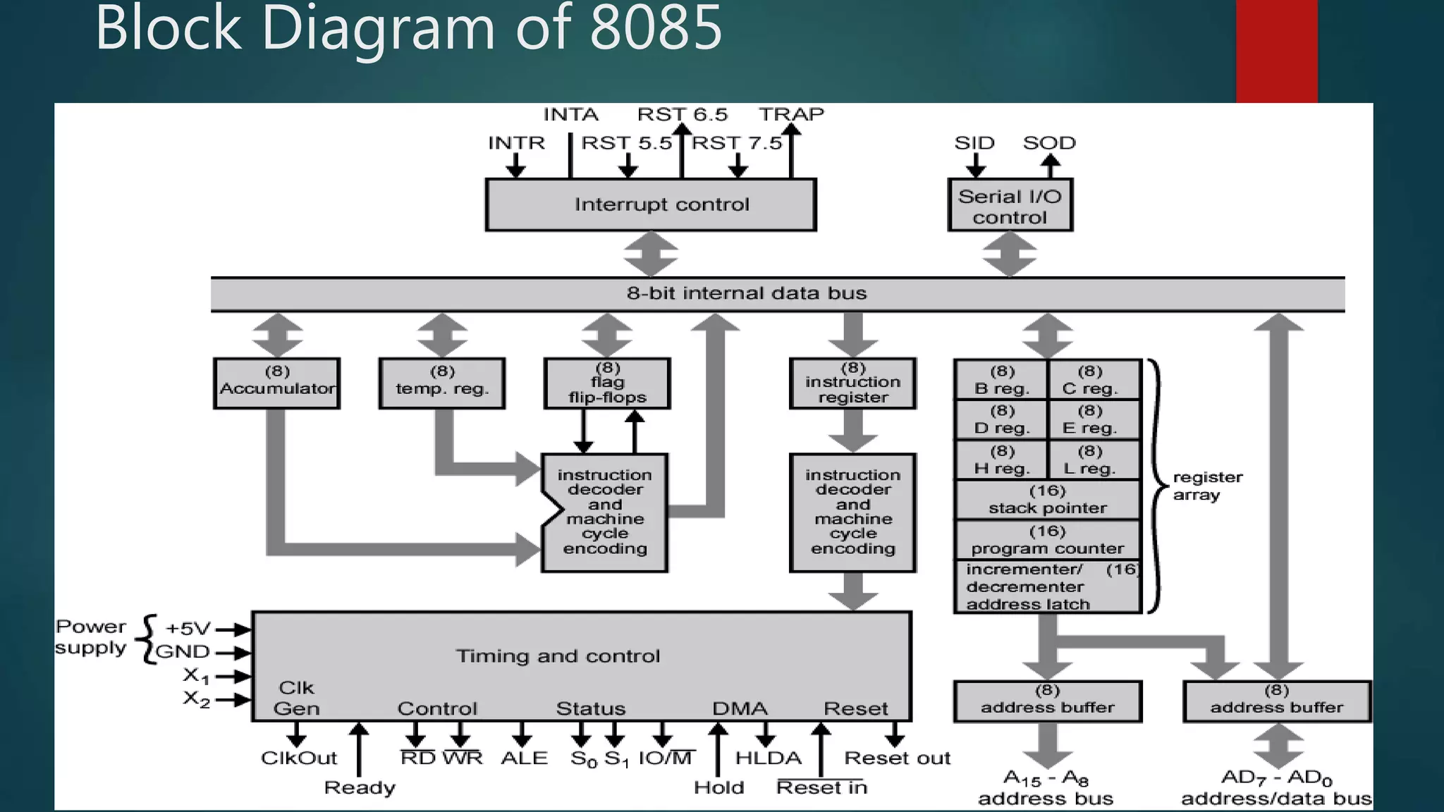
The document describes the internal architecture and components of the 8085 microprocessor. It includes the following main units:
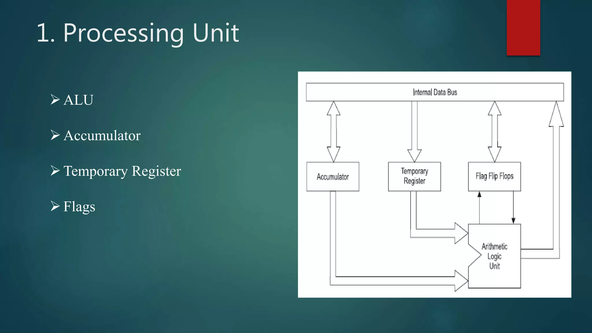
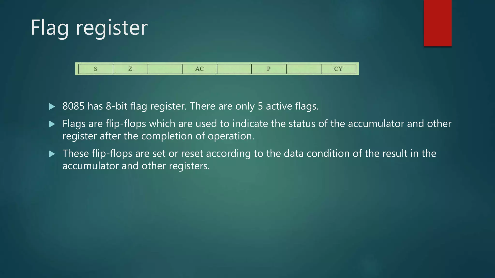
1) Processing unit containing the arithmetic logic unit (ALU), accumulator, flags register, and temporary register for performing arithmetic and logical operations.
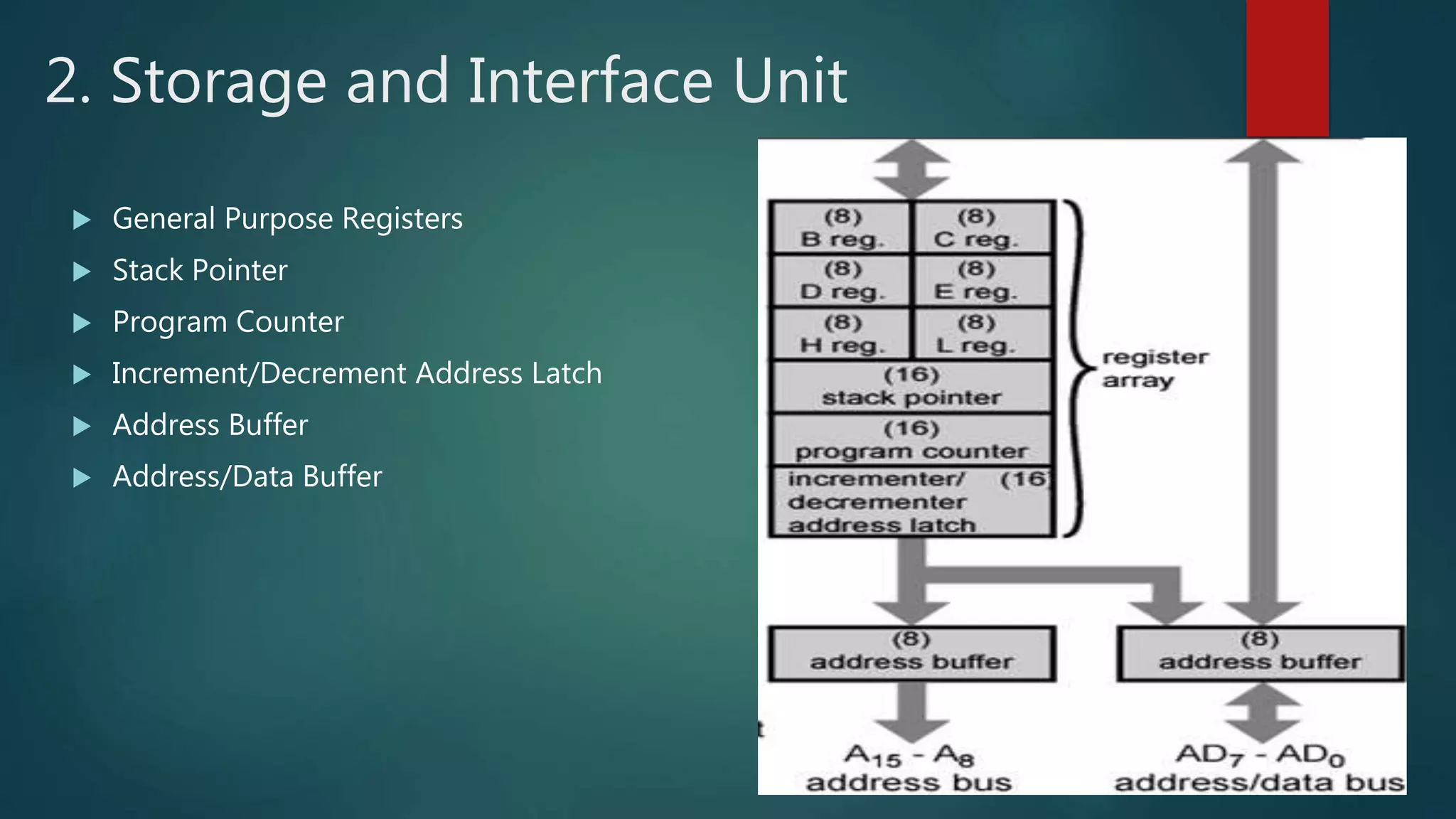
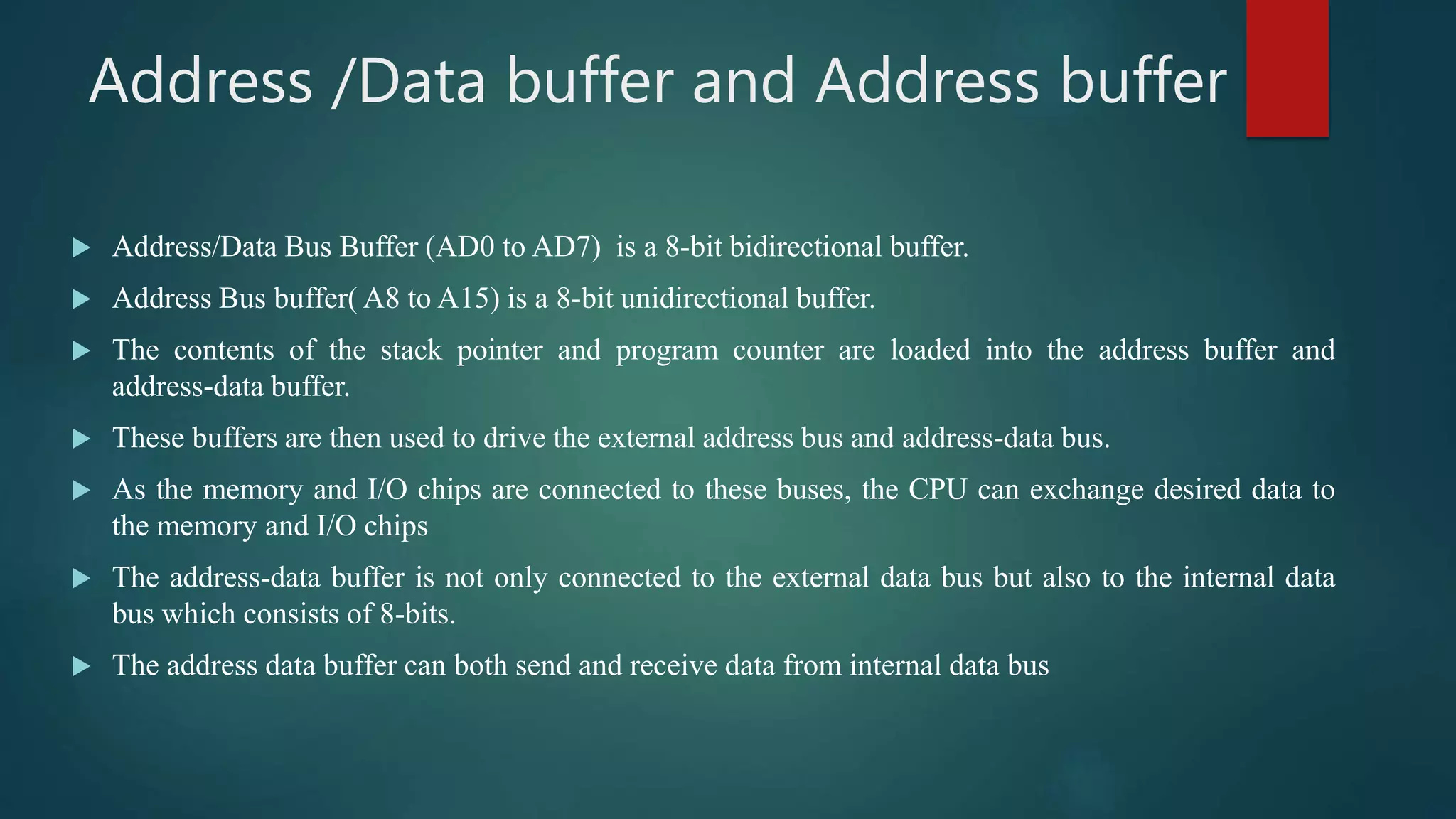
2) Storage and interface unit containing registers like the general purpose registers, stack pointer, program counter, and address/data buffers for memory interfacing.
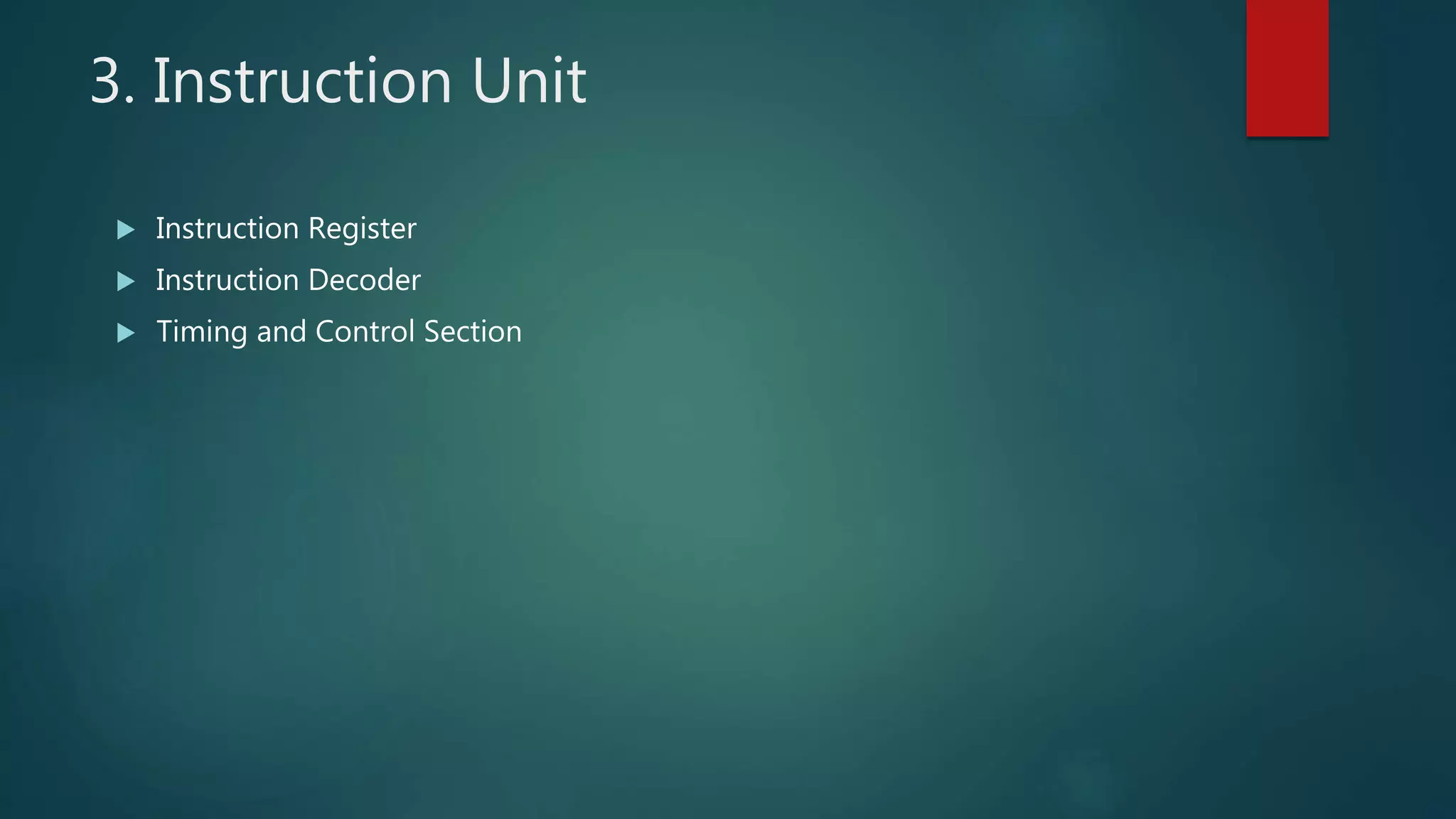
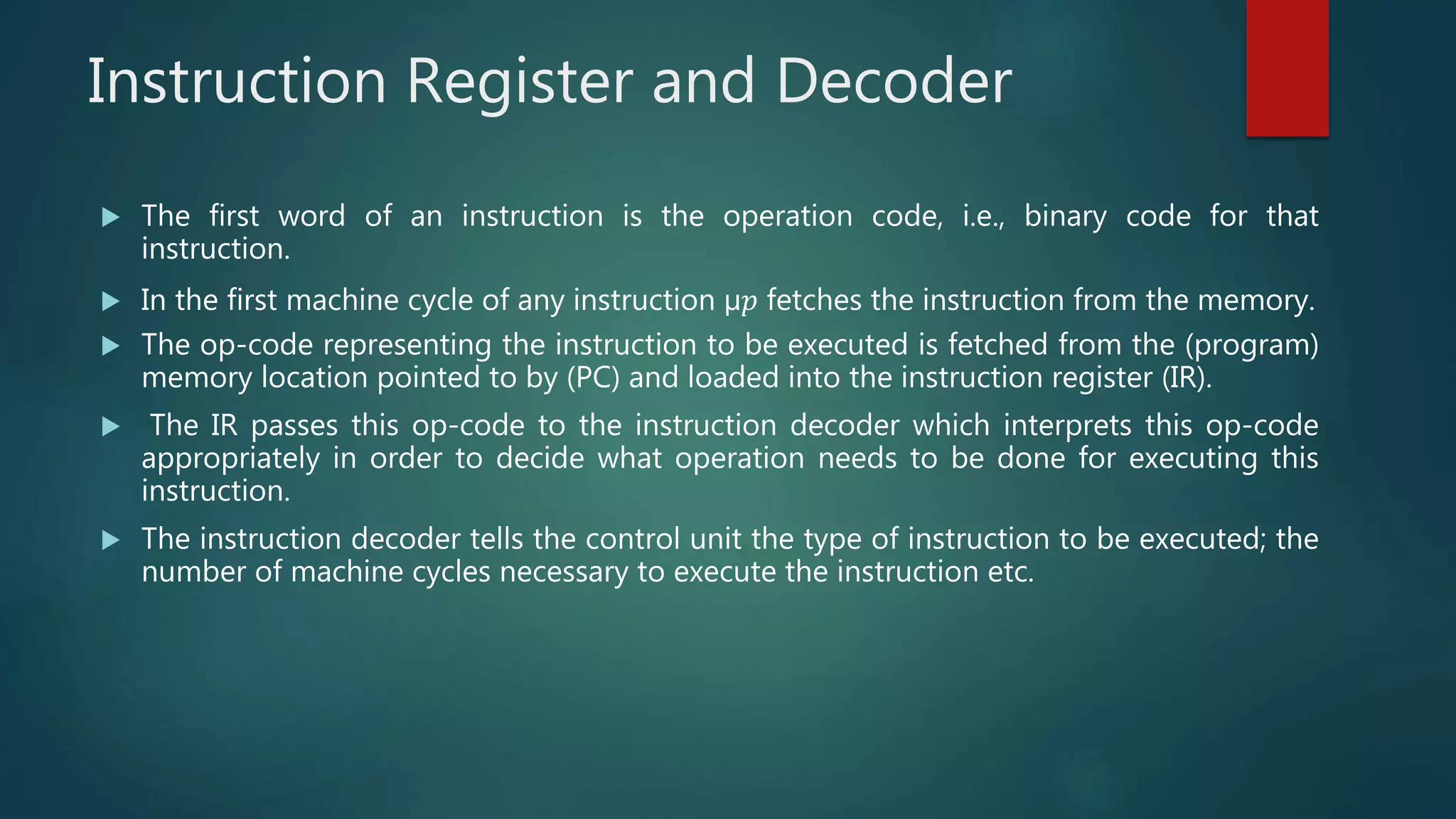
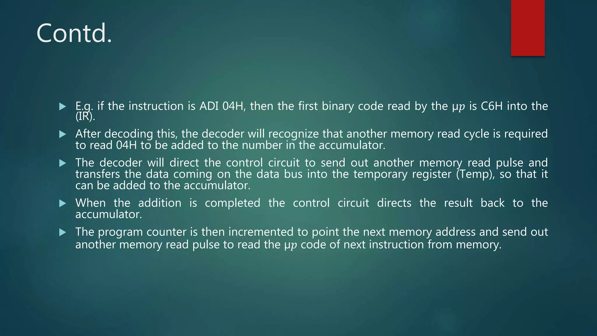
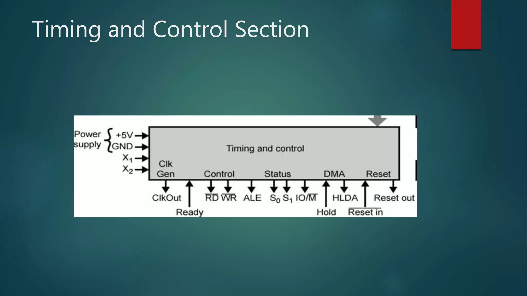
3) Instruction unit containing the instruction register, decoder and timing/control section for fetching and decoding instructions.
4) Interrupt and serial I/O unit for handling interrupts and serial communication with peripheral devices. The 8085 uses address, data and control buses to interface with external memory and devices.