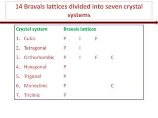
The document discusses different types of solids and crystal structures. It begins by stating that everything around us is matter, which is made of molecules and exists in four main types. It then discusses crystalline and amorphous solids, and the key differences between them. Crystalline solids like metals can have either a single crystal or polycrystalline structure. The document also covers various crystal structures like simple cubic, body centered cubic, face centered cubic, and diamond cubic. It defines important concepts such as unit cell, lattice points, Miller indices, coordination number and packing factor.


![x
y
z
p
x
z
p
y
2r
a/4
a/4
a/4
From the triangle xyp
xy2 = yp2 + px2
xy2 = (a/4)2 + (a/4)2
xy2 = 2(a/4)2
(1)
From the triangle xyz
xz2 = xy2 + yz2
(2r)2 = 2(a/4)2 + (a/4)2
4r2 = 3a2/16
r = a / 8
[Substituted eq. (1) here]](https://image.slidesharecdn.com/1-crystallography-221112052402-80ac2eef/85/1-Crystallography-pptx-32-320.jpg)


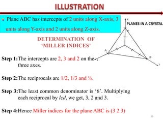
![ In crystal analysis, it is essential to indicate certain directions
inside the crystal.
Suppose we want to indicate the direction OP as shown in Fig.
x, y and z are the crystallographic axes. If a, b and c represent unit
translational vectors along x, y and z directions, then moving u
times ‘a’ along x-axis, v times ‘b’ along y-axis and w times ‘c’
along z-axis, we can reach P. If u, v and w are the smallest integers,
the direction OP indicated by [uvw].
p](https://image.slidesharecdn.com/1-crystallography-221112052402-80ac2eef/85/1-Crystallography-pptx-35-320.jpg)


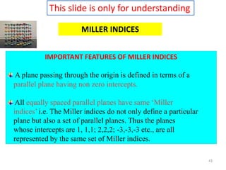
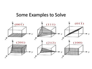
![ When a plane is parallel to any axis, the intercept of the plane on
that axis is infinity. Hence its Miller index for that axis is zero.
When the intercept of a plane on any axis is negative a bar is put on
the corresponding Miller index.
All equally spaced parallel planes have the same index number
(h k l).
If the plane passes through origin, it is defined in terms of a
parallel plane having non-zero intercept.
If a normal is drawn to a plane (h k l), the direction of the normal is
[h k l]](https://image.slidesharecdn.com/1-crystallography-221112052402-80ac2eef/85/1-Crystallography-pptx-40-320.jpg)


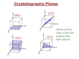


![[010]
[100]
[001]
[110]
[101]
[011]
[110] [111]
Procedure as before:
• (Coordinates of the final point coordinates of the initial point)
• Reduce to smallest integer values
Important directions in 3D represented by Miller Indices (cubic lattice)
Face diagonal
Body diagonal
X
Y
Z
Memorize these](https://image.slidesharecdn.com/1-crystallography-221112052402-80ac2eef/85/1-Crystallography-pptx-61-320.jpg)