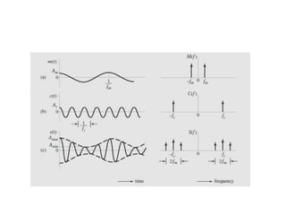
1. The document discusses amplitude modulation (AM) techniques such as AM double sideband full carrier (AMDSB-FC), AM double sideband suppressed carrier (AMDSB-SC), and single sideband (SSB) modulation.
2. It explains that AMDSB-FC and AMDSB-SC use two sidebands which contain redundant information, wasting channel bandwidth. SSB modulation suppresses one sideband to improve bandwidth efficiency.
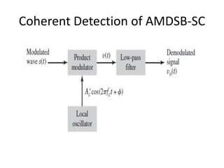
3. Key aspects of envelope detection and its use in demodulating AM signals are covered, along with the need for coherent detection of AMDSB-SC to avoid phase errors.


![• c(t)=𝐴𝑐cos 2𝜋𝑓𝑐t is carrier
• m(t) is message
• AM DSB FC is
• m(t) c(t)+c(t)
• m(t) 𝐴𝑐cos 2𝜋𝑓𝑐t+𝐴𝑐cos 2𝜋𝑓𝑐t
• 𝐴𝑐cos 2𝜋𝑓𝑐t[m(t)+1]
• 𝑠 𝑡 = 𝐴𝑐[1+m(t)] cos 2𝜋𝑓𝑐t
• m(t) cos 2𝜋𝑓𝑐t+𝐴𝑐cos 2𝜋𝑓𝑐t](https://image.slidesharecdn.com/adc1-240321140757-e60f20a6/85/Analog-and-Digital-Communication_ADC-pptx-3-320.jpg)
![• Envelope of s(t) has same shape as m(t) if the
following conditions are satisfied.
• 1. 𝑚(𝑡) < 1
• If this condition is fulfilled 1+m(t) will be more
than 0. In this condition 𝑠 𝑡 = 𝐴𝑐[1+m(t)] will be
positive.
• If 1+m(t)< 0 for some duration, when m(t)
crosses zero there will be phase reversal, which
means there is distortion. This condition is called
overmodulation.](https://image.slidesharecdn.com/adc1-240321140757-e60f20a6/85/Analog-and-Digital-Communication_ADC-pptx-4-320.jpg)

![2. The carrier frequency 𝑓𝑐 ≫ 𝑊 where W is message
bandwidth.
m(t) 𝐴𝑐cos 2𝜋𝑓𝑐t+𝐴𝑐cos 2𝜋𝑓𝑐t
m(t)=a 𝑚𝑛(t) where a=
𝑚(𝑡) 𝑚𝑎𝑥
𝐴𝑐
is called modulation index
and 𝑚𝑛(t) is called normalised modulating signal where its
minimum value is
-1.
𝑚𝑛 𝑡 =
m(t)
𝑚(𝑡) 𝑚𝑎𝑥
𝑠 𝑡 = 𝐴𝑐[1+ a 𝑚𝑛(t) ] cos 2𝜋𝑓𝑐t
𝑠 𝑡 = 𝐴𝑐[1+ 𝑘𝑎 𝑚 (t) ] cos 2𝜋𝑓𝑐t, where 𝑘𝑎=1/𝐴𝑐
𝑘𝑎 is called amplitude sensitivity](https://image.slidesharecdn.com/adc1-240321140757-e60f20a6/85/Analog-and-Digital-Communication_ADC-pptx-6-320.jpg)


![• Consider a modulating wave that consists of a single
tone or frequency component;
that is,
m(t)=𝐴𝑚cos 2𝜋𝑓𝑚t
AM wave is therefore given by
𝑠 𝑡 = 𝐴𝑐[1+ a cos 2𝜋𝑓𝑚t ] cos 2𝜋𝑓𝑐t
𝐴𝑚𝑎𝑥
𝐴𝑚𝑖𝑛
=
𝐴𝑐(1+𝑎)
𝐴𝑐(1−𝑎)
This equation gives
a=
𝐴𝑚𝑎𝑥−𝐴𝑚𝑖𝑛
𝐴𝑚𝑎𝑥+𝐴𝑚𝑖𝑛](https://image.slidesharecdn.com/adc1-240321140757-e60f20a6/85/Analog-and-Digital-Communication_ADC-pptx-11-320.jpg)
![• 𝑠 𝑡 = 𝐴𝑐[1+ a cos 2𝜋𝑓𝑚t ] cos 2𝜋𝑓𝑐t
= 𝐴𝑐 cos 2𝜋𝑓𝑐t+ a 𝐴𝑐 cos 2𝜋𝑓𝑚t cos 2𝜋𝑓𝑐t
= 𝐴𝑐 cos 2𝜋𝑓𝑐t+
a 𝐴𝑐
2
cos 2𝜋 (𝑓𝑐− 𝑓𝑚)t+
a 𝐴𝑐
2
cos 2𝜋 (𝑓𝑐+𝑓𝑚)t
S(f)=
𝐴𝑐
2
𝛿(𝑓 + 𝑓𝑐)+
𝑎𝐴𝑐
4
𝛿(𝑓 + [𝑓𝑐−𝑓𝑚])+
𝑎𝐴𝑐
4
𝛿(𝑓 −
[𝑓𝑐−𝑓𝑚])+
𝑎𝐴𝑐
4
𝛿(𝑓 + [𝑓𝑐−𝑓𝑚])+
𝑎𝐴𝑐
4
𝛿(𝑓 +
[𝑓𝑐+𝑓𝑚])+
𝑎𝐴𝑐
4
𝛿(𝑓 − [𝑓𝑐+𝑓𝑚])](https://image.slidesharecdn.com/adc1-240321140757-e60f20a6/85/Analog-and-Digital-Communication_ADC-pptx-12-320.jpg)
![• Signal power in carrier=
𝐴𝑐
2
2
•
[
𝑎2𝐴𝑐
4
2
]
2
=
𝑎2𝐴𝑐
8
2
•
[
𝑎2𝐴𝑐
4
2
]
2
=
𝑎2𝐴𝑐
8
2
• The ratio of the total sideband power to the total power in
the modulated wave is equal to
𝑎2
2+𝑎2 which depends only
on the modulation factor.
• If 100 percent modulation is used the total power in the
two side frequencies of the resulting AM wave is only one-
third of the total power in the modulated wave.](https://image.slidesharecdn.com/adc1-240321140757-e60f20a6/85/Analog-and-Digital-Communication_ADC-pptx-14-320.jpg)