Download to read offline
![EXPERIMENTAL WIDEBAND CHARACTERIZATION OF A PARALLEL-PLATE CAPACITOR: VNA VS TDR COMPARISON Piero Belforte Feb 1 2021
1
A parallel-plate capacitor implemented by a rectangular double-sided printed circuit board (p.c.b.) is
characterized by means a stimulus signal injected at a corner. Both frequency-domain (VNA) and
time-domain (TDR) techniques are utilized to determine the step response of the reflected wave
(S11) to be compared to the theoretical behavior of the equivalent parallel plate capacitance. A
commercial application is utilized to convert the frequency domain tabulated data of the frequency
response into the corresponding TDR response. A simple, very accurate and fast 2D TLM
(Transmission Line Model) model can be easily extracted from these single time-domain
experimental responses. This kind of models can be utilized to simulate very efficiently the Power
Distribution Networks of p.c.b.s [2] using the Digital Wave Simulator (DWS) [3]
Figure 1
Calculation of theoretical capacitance taking into account the dimensions of the p.c.b.
under test. Two values of FR4 relative dielectric constant Er are taken into acccount:4.7
and 4.9. From the http://www.calctool.org/CALC/eng/electronics/parallel_plate website.](https://image.slidesharecdn.com/3experimentalwidebandcharacterizationofaparallel-platecapacitor-210205122509/75/3-experimental-wideband_characterization_of_a-parallel-plate_capacitor-1-2048.jpg)
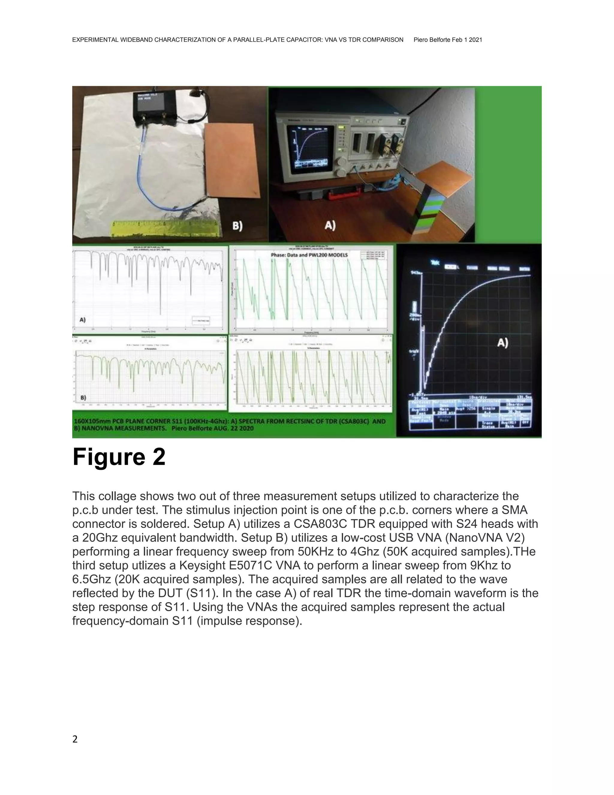
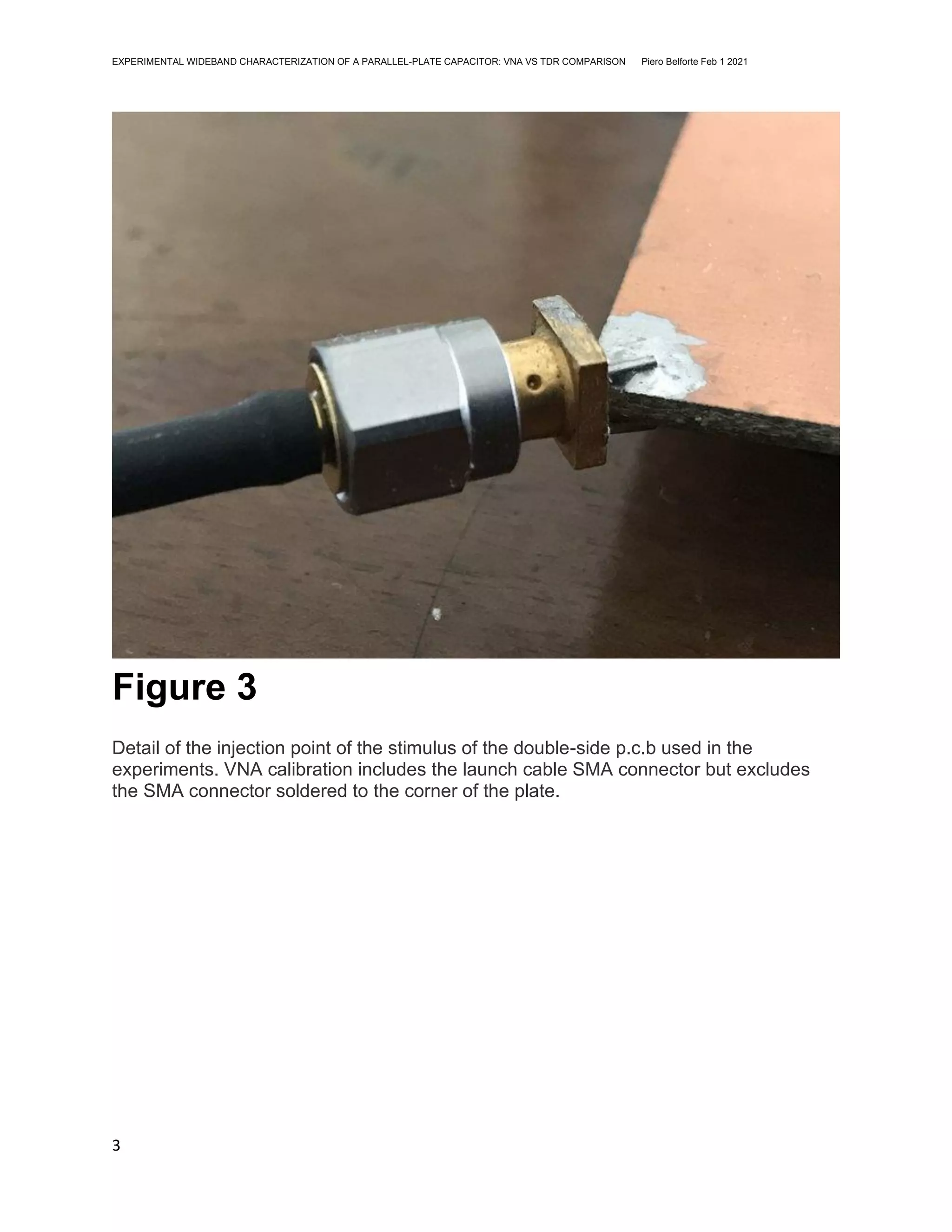
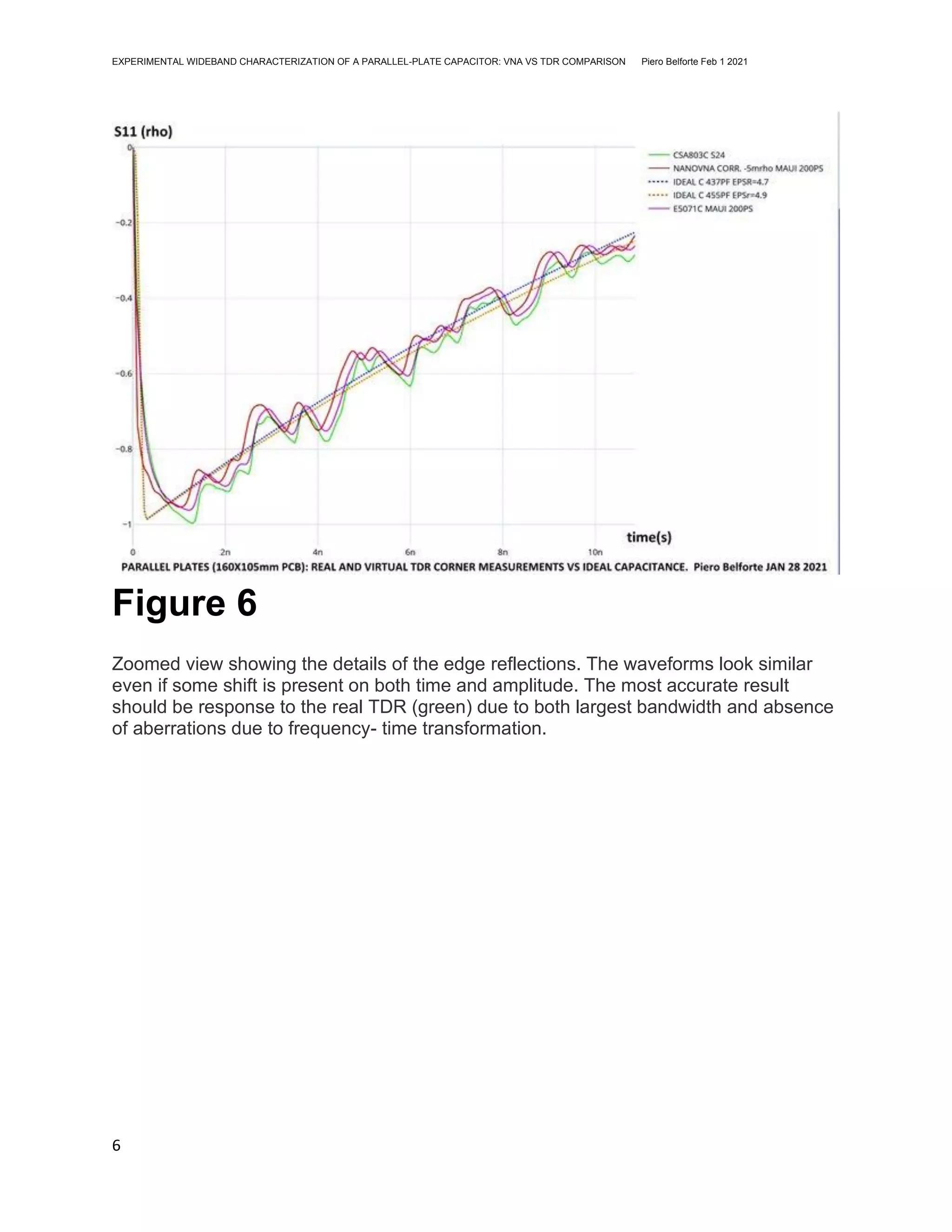
![EXPERIMENTAL WIDEBAND CHARACTERIZATION OF A PARALLEL-PLATE CAPACITOR: VNA VS TDR COMPARISON Piero Belforte Feb 1 2021
4
Figure 4
Comparison between the S11 step responses obtained from the measurements and the
theoretical ideal capacitors simulated by DWS. The tabulated frequency responses of
the VNAs (touchstone files .s1p) are converted into the step responses by means of the
MAUI application available from Teledyne Lecroy [4]. In this case the equivalent step
risetime is set to 200ps to minimize the ringing of the transformed waveform. MAUI
calculates the voltage at the injection port V1 instead of the reflected waveform. Some
additional calculation is needed: in particular a unity value is subtracted from V1
samples. Moreover the initial samples with negative time values are deleted. The overall
behaviors look very similar. The measured responses are characterized by reflections
occurring at the edges of the p.cb. . The static capacitance calculated using the
theoretical formula matches the experimental measurements, obvioulsly excluding the
reflections. The fringe capacitance effect is negligible on the static value.](https://image.slidesharecdn.com/3experimentalwidebandcharacterizationofaparallel-platecapacitor-210205122509/75/3-experimental-wideband_characterization_of_a-parallel-plate_capacitor-4-2048.jpg)
![EXPERIMENTAL WIDEBAND CHARACTERIZATION OF A PARALLEL-PLATE CAPACITOR: VNA VS TDR COMPARISON Piero Belforte Feb 1 2021
11
Figure 11
Unwrapped phase spectrum of the original response data and the PWL200_OFC
macromodel of S11 calculated by PWLFIT+ from the CSA803C measurement [5].](https://image.slidesharecdn.com/3experimentalwidebandcharacterizationofaparallel-platecapacitor-210205122509/75/3-experimental-wideband_characterization_of_a-parallel-plate_capacitor-11-2048.jpg)
![EXPERIMENTAL WIDEBAND CHARACTERIZATION OF A PARALLEL-PLATE CAPACITOR: VNA VS TDR COMPARISON Piero Belforte Feb 1 2021
12
Figure 12
Comparison of the S11 macromodels calculated using both the PWLFIT and Vector
Fitting (VF) algorithms starting from the actual TDR measurement data. A model order
of 200 is chosen for the comparison. As depicted in the figure, VF performs slightly
better on spectrum error but shows a time-domain rms error abot one order of
magnitude larger. than PWLFIT. In the DWS implementation the PWL200 is about 20X
faster than VF200 and more stable due to the FIR implementation. [1]](https://image.slidesharecdn.com/3experimentalwidebandcharacterizationofaparallel-platecapacitor-210205122509/75/3-experimental-wideband_characterization_of_a-parallel-plate_capacitor-12-2048.jpg)
![EXPERIMENTAL WIDEBAND CHARACTERIZATION OF A PARALLEL-PLATE CAPACITOR: VNA VS TDR COMPARISON Piero Belforte Feb 1 2021
13
Figure 13
An example of accurate wideband and very fast model of the parallel plate capacitor as a grid of
lossy Transmission Lines. Only 5 parameters are needed to describe this model that can be
extracted from a single TDR measurement. This kind of 2D lossy TLM models can be applied for
example in the prediction of the noise generated by switching drivers on actual p.c.b. boards [2], [3]](https://image.slidesharecdn.com/3experimentalwidebandcharacterizationofaparallel-platecapacitor-210205122509/75/3-experimental-wideband_characterization_of_a-parallel-plate_capacitor-13-2048.jpg)
![EXPERIMENTAL WIDEBAND CHARACTERIZATION OF A PARALLEL-PLATE CAPACITOR: VNA VS TDR COMPARISON Piero Belforte Feb 1 2021
14
References
[1] Piero Belforte et aliii : Automated Framework for Time-Domain Piecewise- Linear Fitting Method
Based on Digital Wave Processing of S-Parameters IEEE Transactions on Circuits and Systems Jan. 2020
https://www.researchgate.net/publication/336912388_Automated_Framework_for_Time-
Domain_Piecewise-_Linear_Fitting_Method_Based_on_Digital_Wave_Processing_of_S-Parameters
[2] Piero Belforte: PCB PLANE, INTERCONNECT SWITCHING NOISE
SIMULATION,https://www.researchgate.net/publication/281714186_SpicySWAN_report_PCB_PLANE_I
NTERCONNECT_SWITCHING_NOISE_SIMULATION
[3] Piero Belforte, Giancarlo Guaschino: DWS 9.0 Digital Wave Simulator,
https://www.researchgate.net/publication/338337640_DWS_90_Digital_Wave_Simulator
[4} Teledyne LeCroy: Oscilloscopes Remote Control and Automation
http://cdn.teledynelecroy.com/files/manuals/maui-remote-control-and-automation-manual.pdf
[5] Piero Belforte et alii: Frequency Domain Behavior of S-Parameters Piecewise-Linear Fitting
in a Digital-Wave Framework, to be published
Content subject to copyright.](https://image.slidesharecdn.com/3experimentalwidebandcharacterizationofaparallel-platecapacitor-210205122509/75/3-experimental-wideband_characterization_of_a-parallel-plate_capacitor-14-2048.jpg)

The document presents a comparison of frequency-domain (VNA) and time-domain (TDR) techniques for characterizing a parallel-plate capacitor using a printed circuit board. It explores the accuracy of the measured responses relative to theoretical models and discusses the impact of calibration and frequency alignment on results. Additionally, it highlights the efficiency of a new 2D TLM model for simulating power distribution networks using data obtained from the experiments.


![Seller Deck - Presentation [Concert L2].PPTX](https://cdn.slidesharecdn.com/ss_thumbnails/sellerdeck-presentationconcertl2-251219171156-24982daf-thumbnail.jpg?width=640&height=640&fit=bounds)


