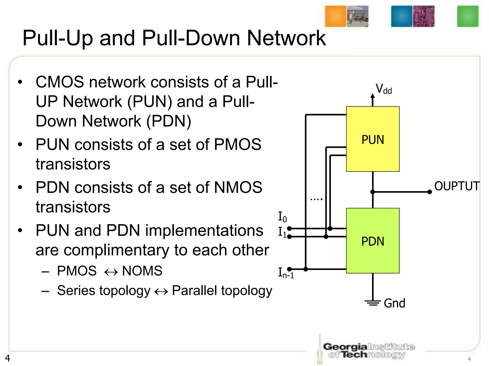
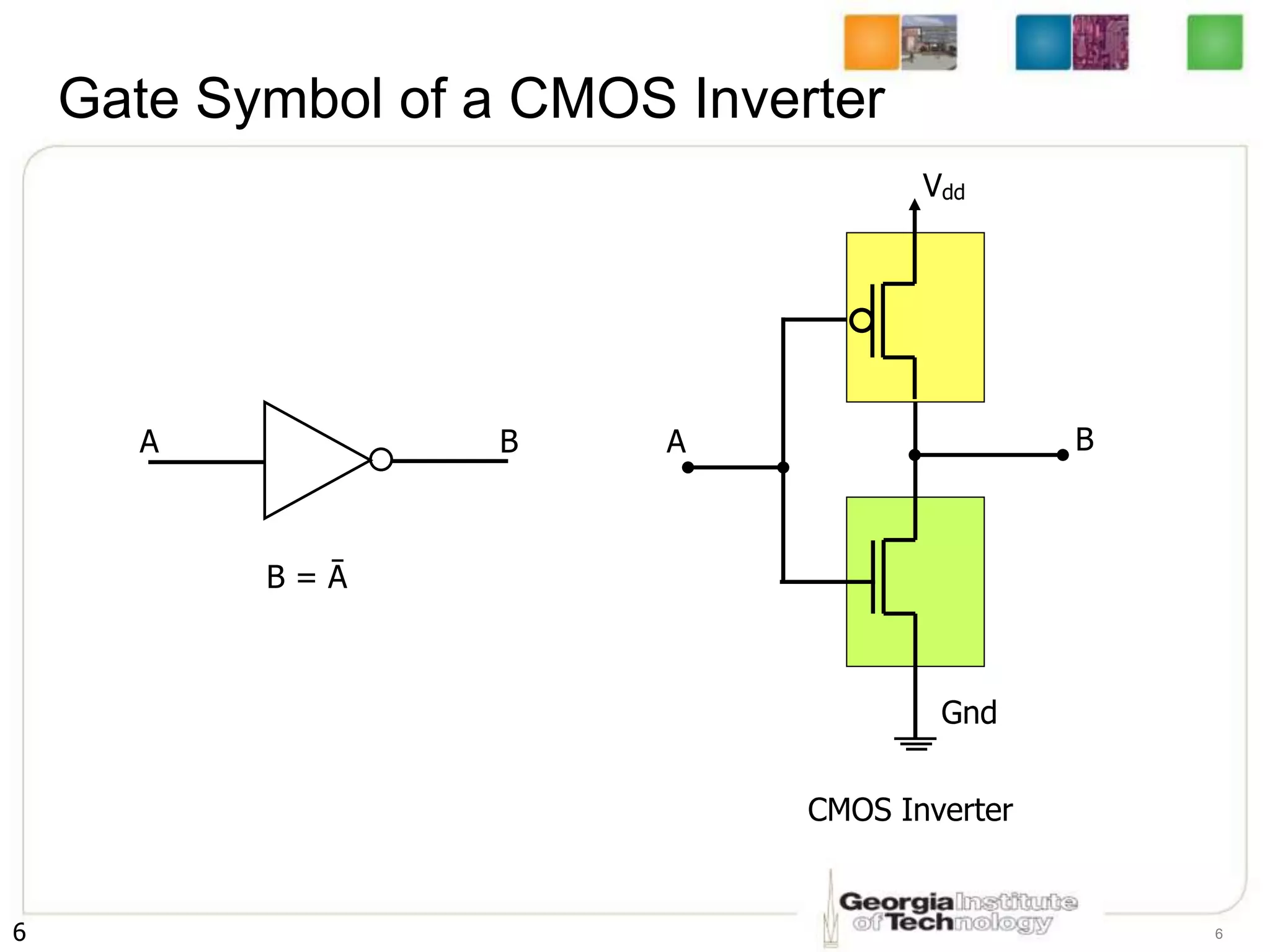
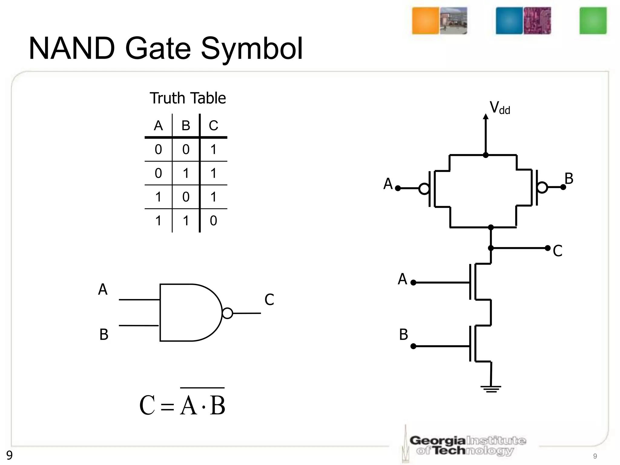
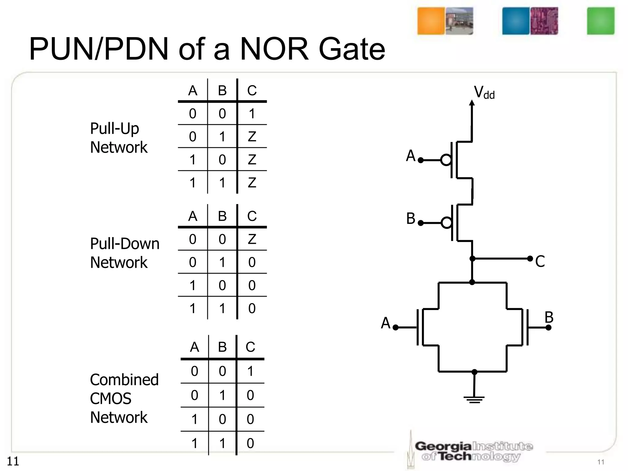
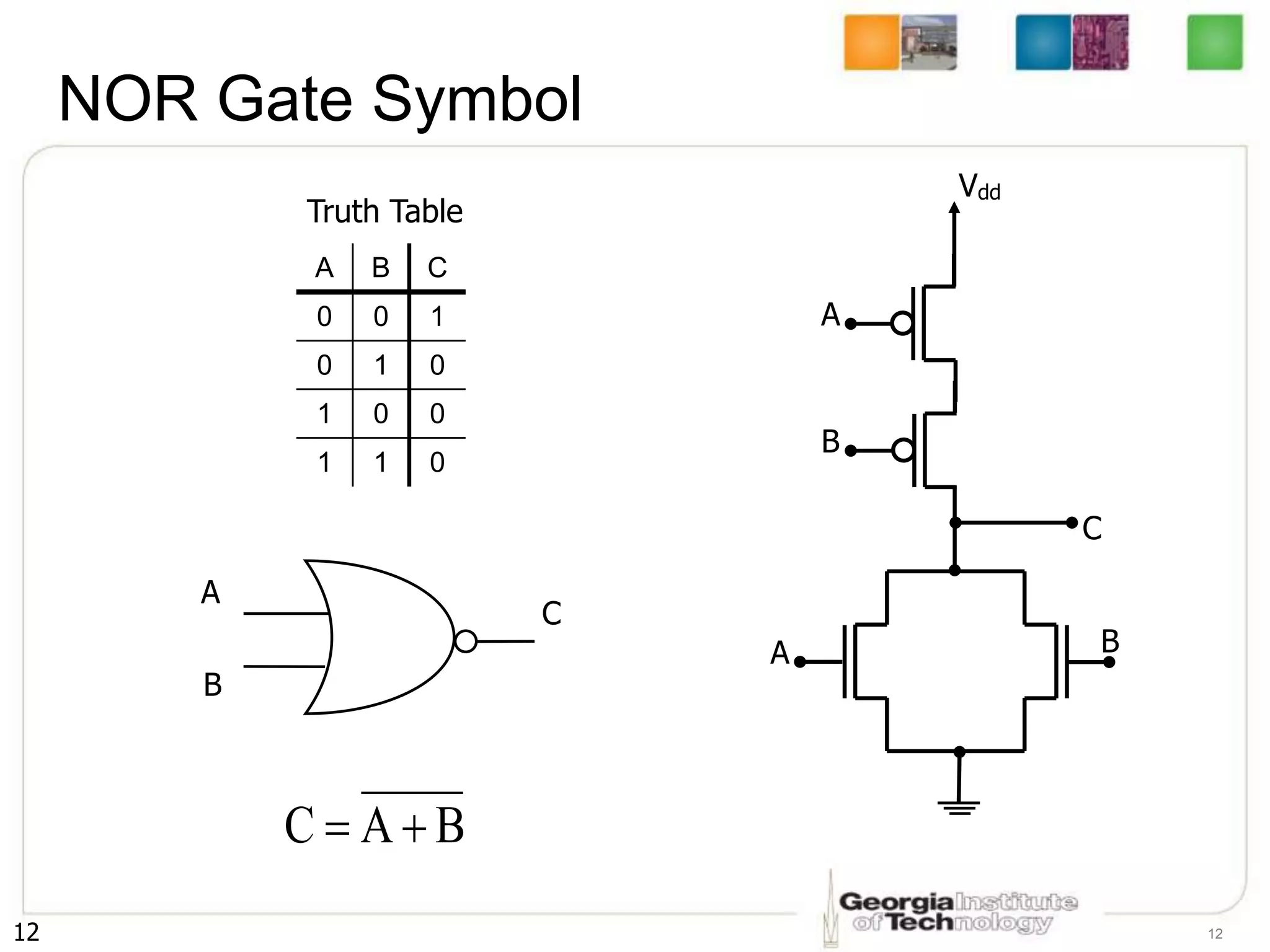
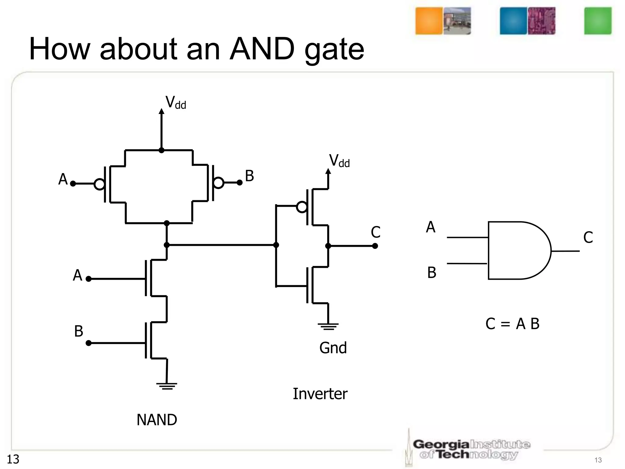
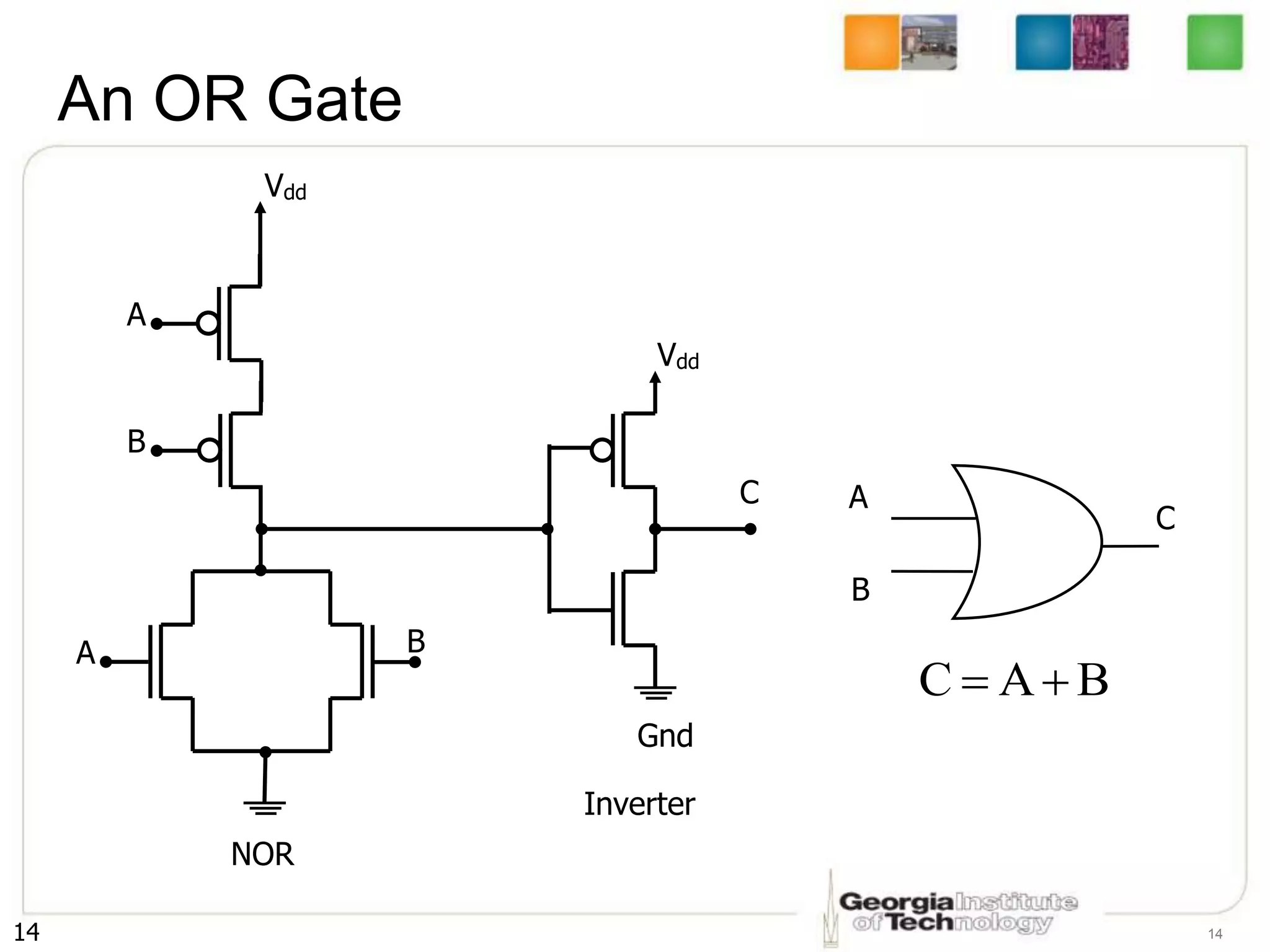
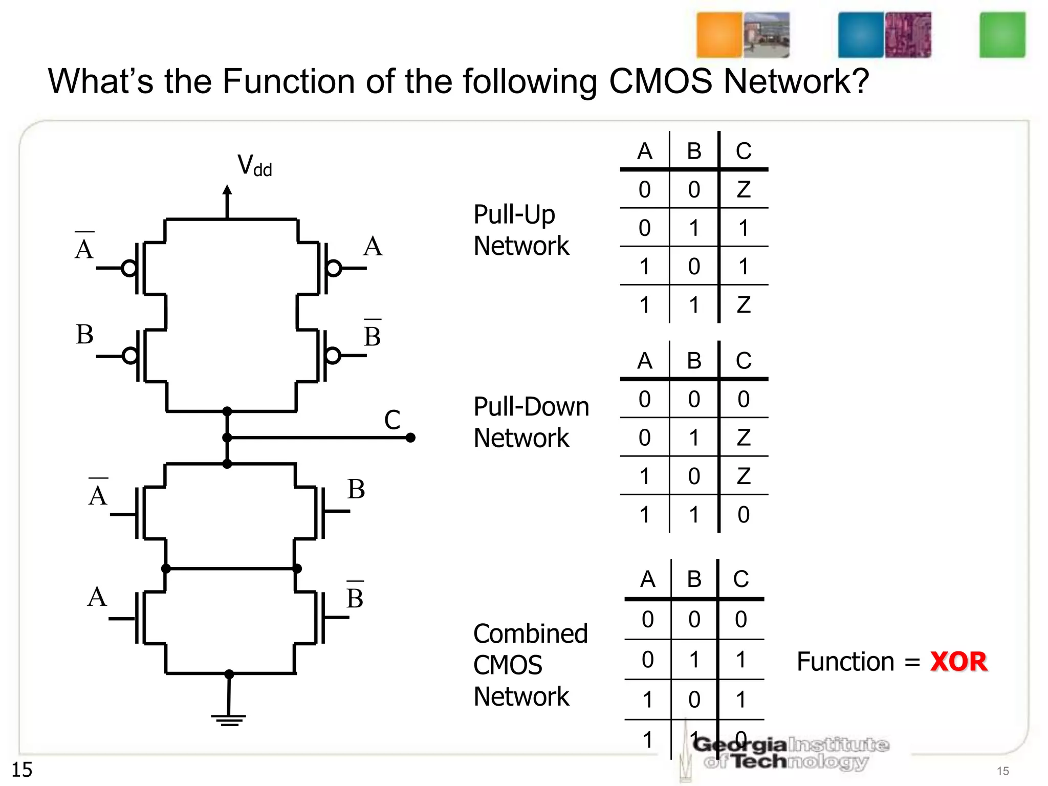
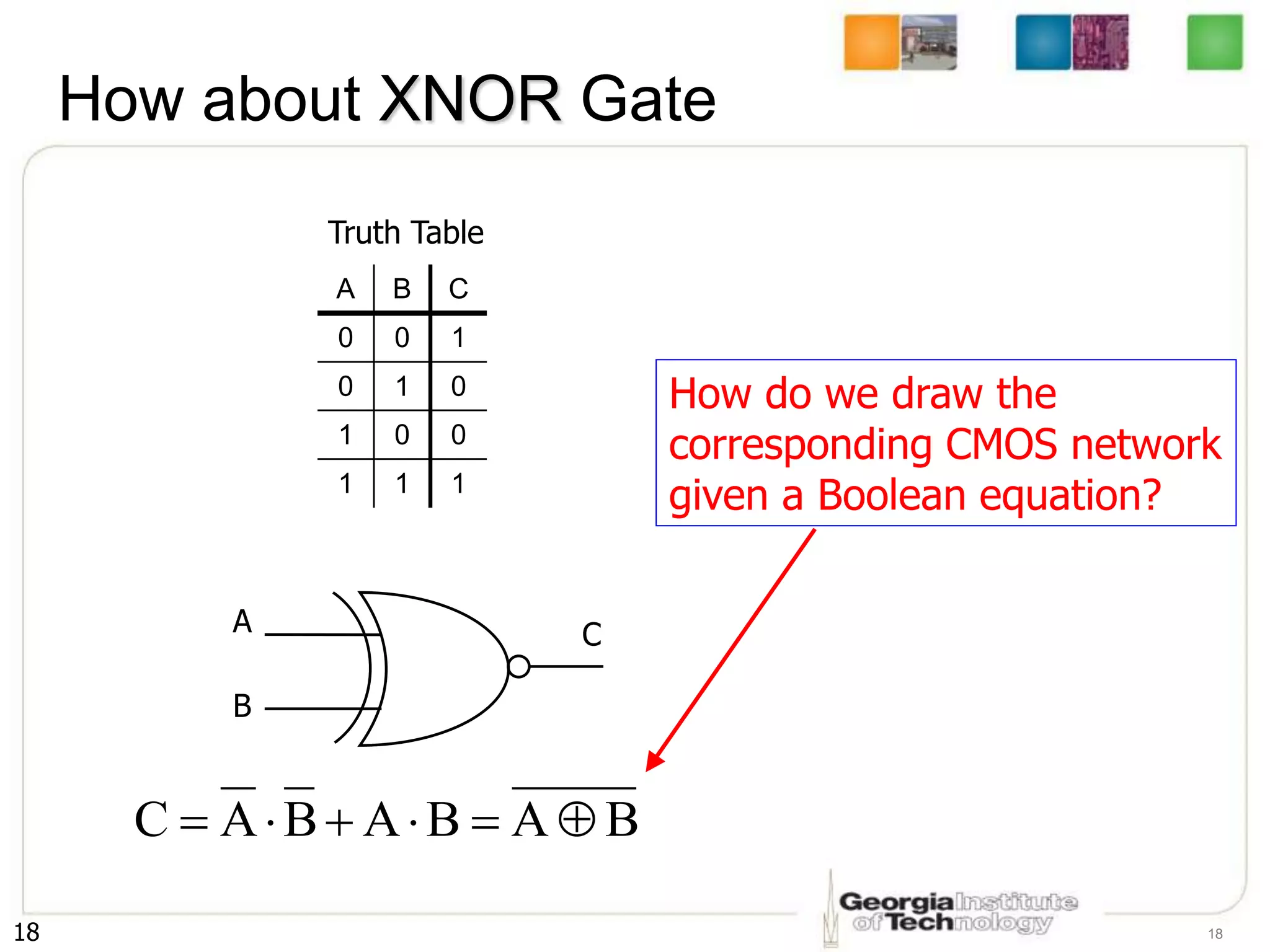
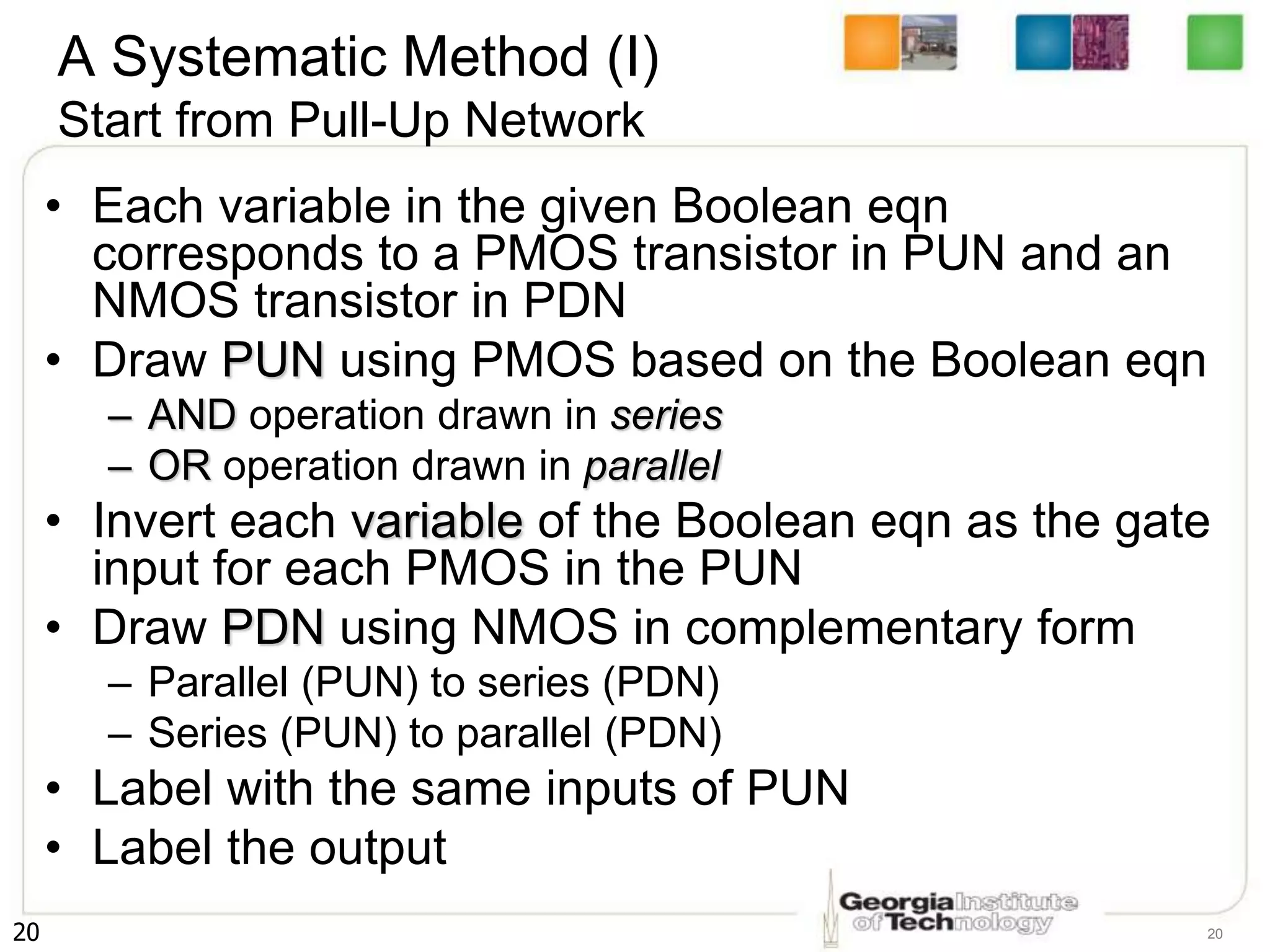
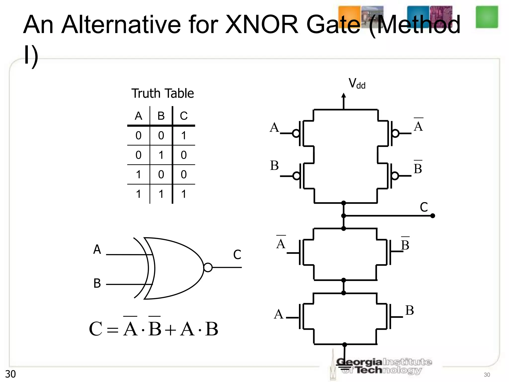
1. The document discusses CMOS inverters and basic gates like NAND and NOR.
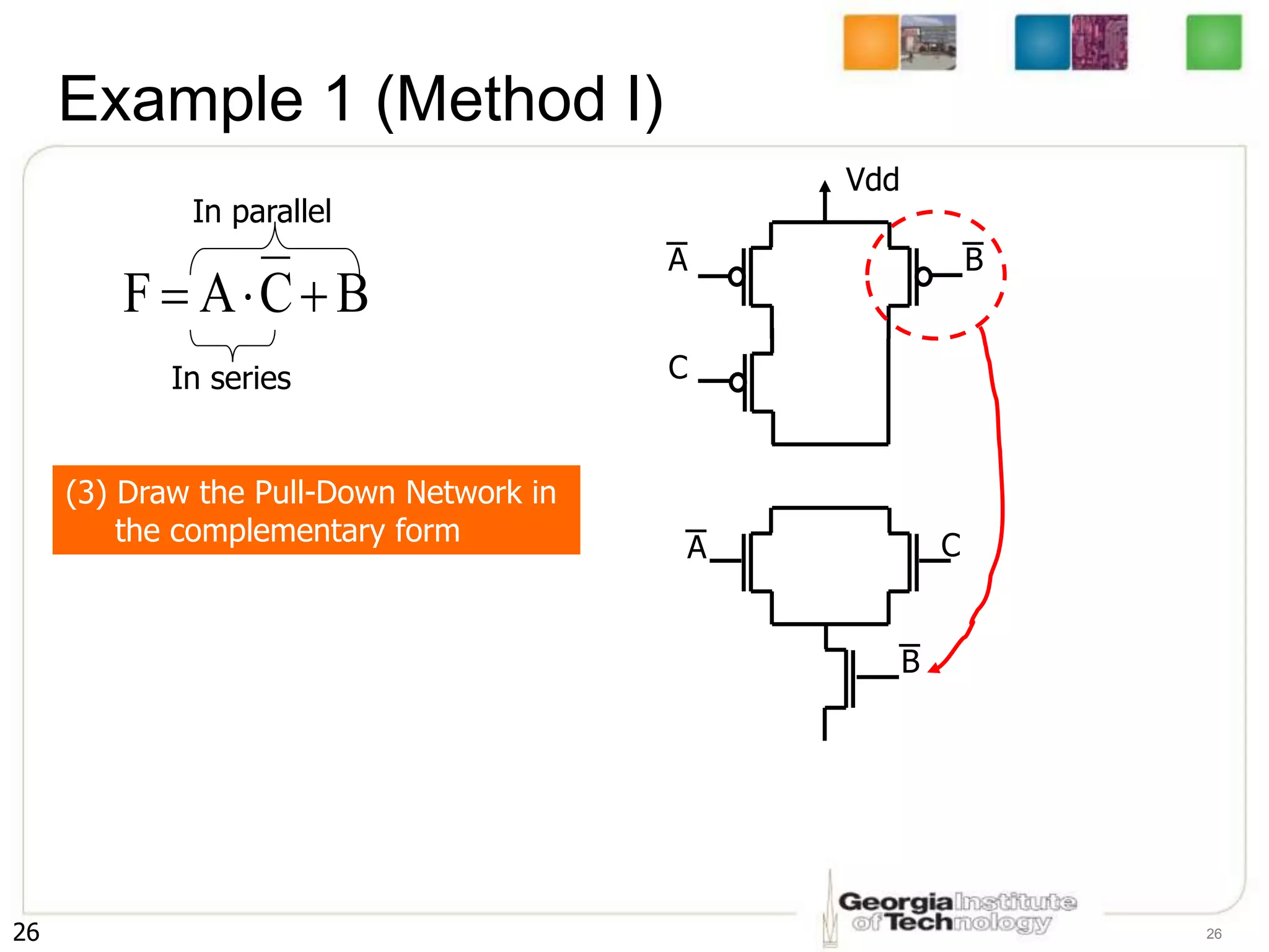
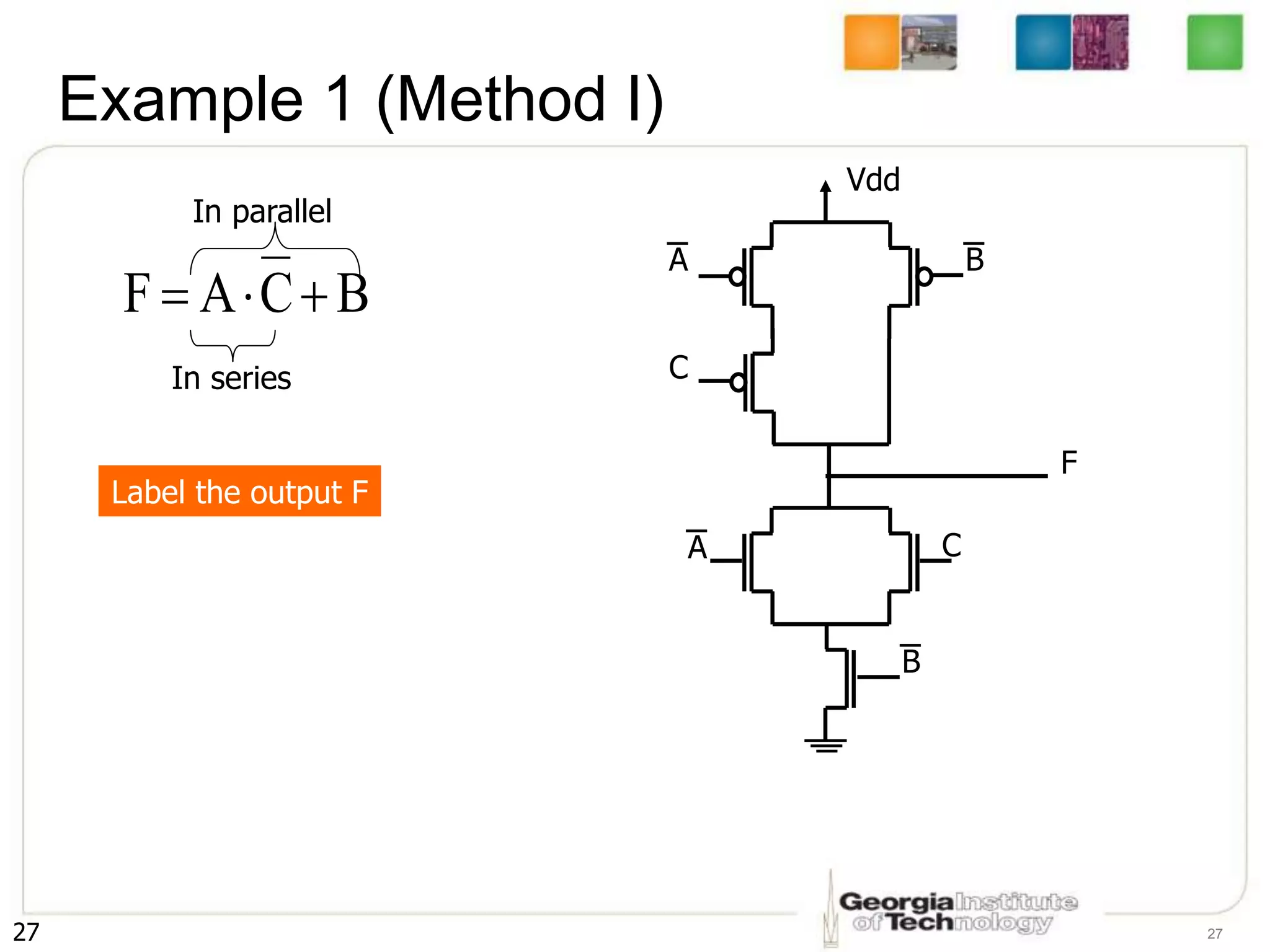
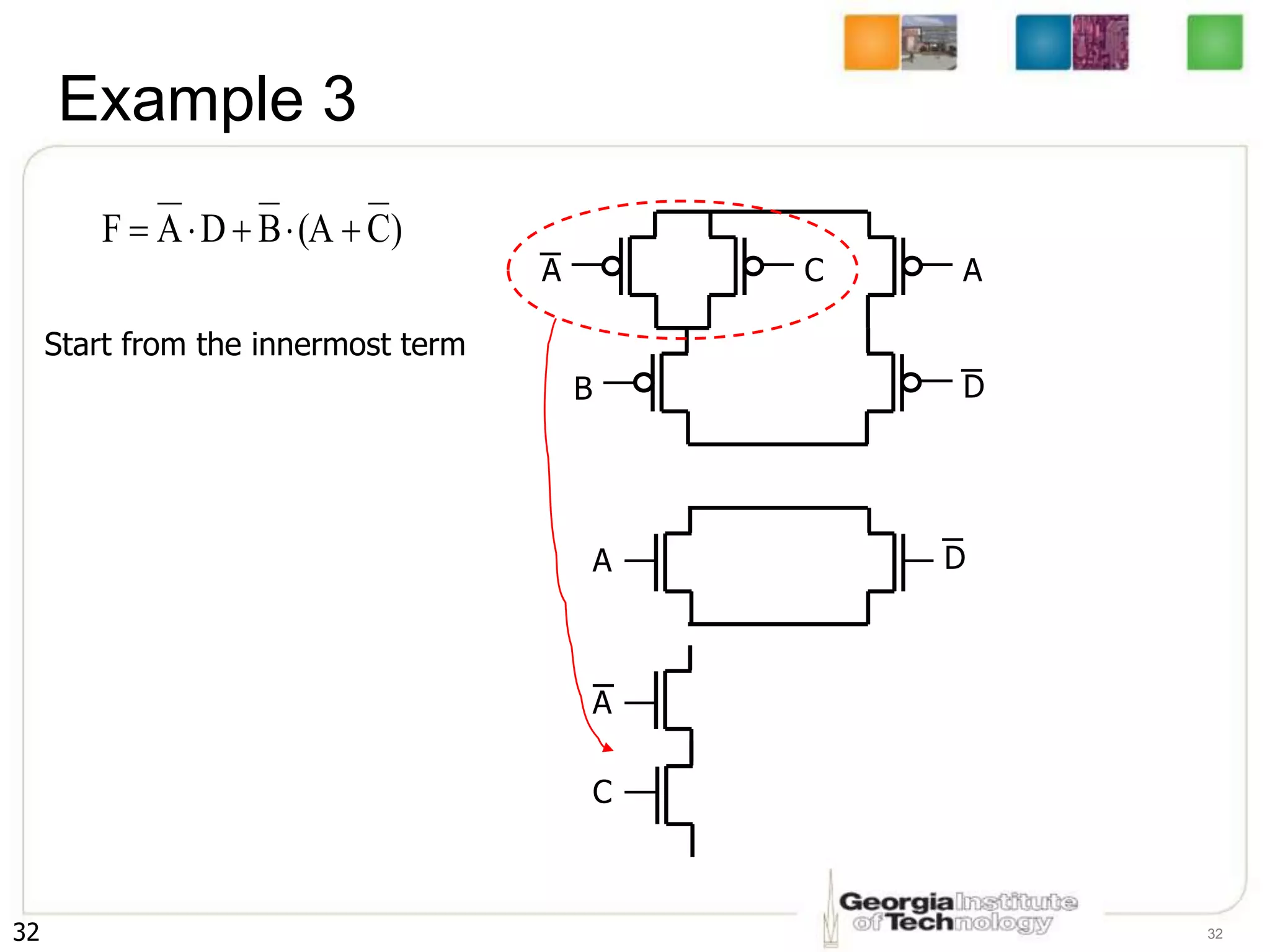
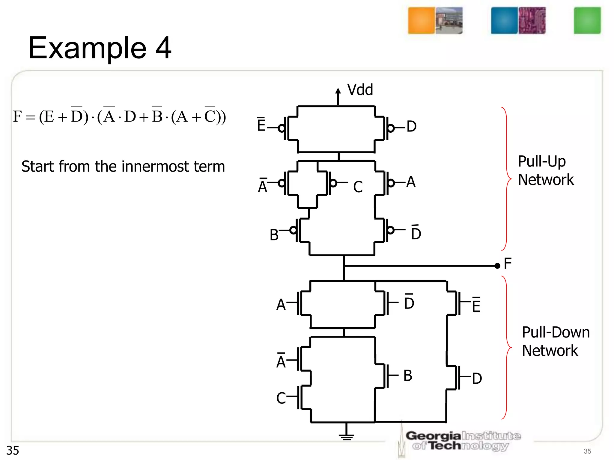
2. It describes how to systematically design the pull-up network and pull-down network that make up a CMOS circuit from a Boolean equation.
3. The key steps are to represent each variable as a transistor, connect transistors in series for AND and parallel for OR, and ensure the pull-up and pull-down networks are complements of each other.


![OzaBagAdwin (OBA) slide [7].pdf](https://cdn.slidesharecdn.com/ss_thumbnails/ozabagadwinobaslide7-220616045854-36004448-thumbnail.jpg?width=640&height=640&fit=bounds)


