Download to read offline
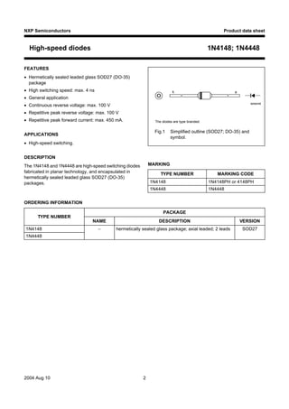
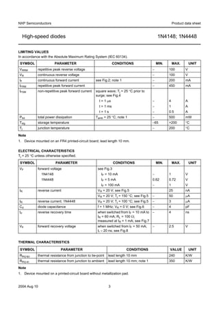

This document provides data sheets for the 1N4148 and 1N4448 high-speed switching diodes. It summarizes their key features and specifications, including maximum voltage and current ratings, packaging details, and thermal and electrical characteristics graphs. The diodes are designed for high-speed switching applications with maximum switching speeds of 4 nanoseconds.