Download to read offline

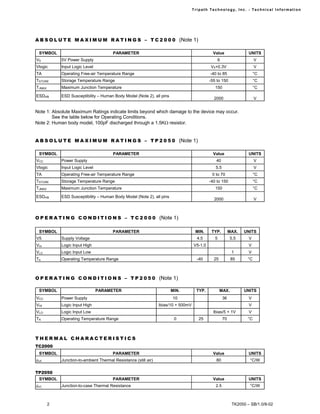

The document provides technical information about the TK2050, a 50W Class-T digital audio amplifier using Tripath's Digital Power Processing technology. It offers high output power of 50W at 8 ohms or less than 1% THD+N and high efficiency of 92% at 60W into 8 ohms. The amplifier integrates the TC2000 audio signal processor and TP2050 power stage driver. It is suitable for applications such as home theater and stereo systems.