Download to read offline

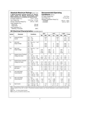
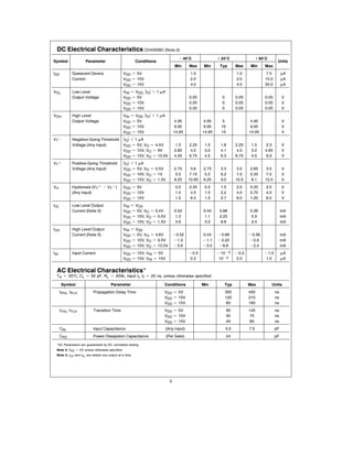
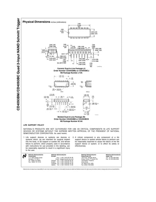

This document provides information on the CD4093BM CD4093BC Quad 2-Input NAND Schmitt Trigger integrated circuit. It consists of four independent Schmitt trigger NAND gates, each with Schmitt trigger hysteresis on both inputs for noise immunity. The IC has a wide supply voltage range of 3-15V, and specifications for propagation delay, input/output voltage levels and currents, and hysteresis are provided over temperature. Typical applications include wave shaping, pulse generation, and logic functions. Dimensions and packaging options are included.