Download to read offline

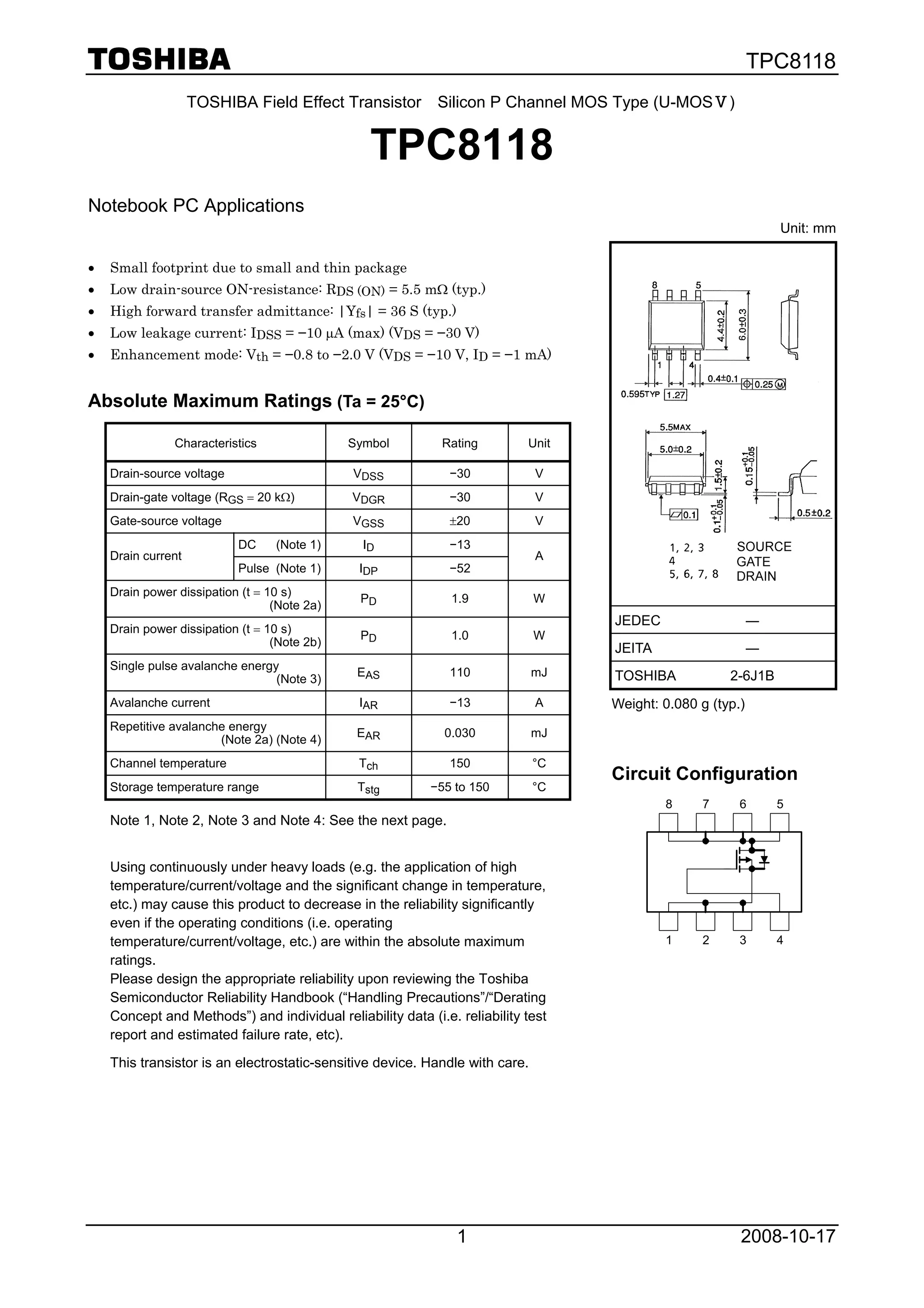
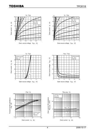
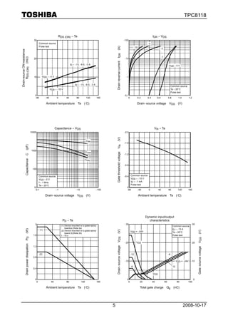
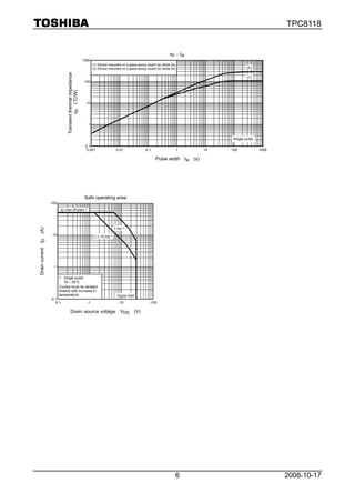

This document provides specifications for the TPC8118 P-channel MOSFET transistor from Toshiba. It is intended for use in notebook PC applications due to its small size and low drain-source on-resistance. Key specifications include a maximum drain-source voltage of -30V, threshold voltage between -0.8V to -2.0V, and on-resistance as low as 5.5mOhms. The document provides detailed absolute maximum ratings, electrical characteristics, and switching behavior parameters.