1. GaAs MMIC CF 750
Data Sheet
• Biased Dual Gate GaAs FET
• For frequencies from 400 MHz to 3 GHz
• For mixer and amplifier applications, i.e LNA- and
buffer stages in handheld equipment
• Low power consumption, 2 mA operating current
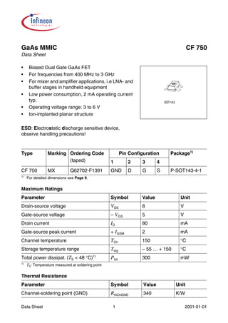
typ. SOT-143
• Operating voltage range: 3 to 6 V
• Ion-implanted planar structure
ESD: Electrostatic discharge sensitive device,
observe handling precautions!
Type Marking Ordering Code Pin Configuration Package1)
(taped) 1 2 3 4
CF 750 MX Q62702-F1391 GND D G S P-SOT143-4-1
1)
For detailed dimensions see Page 9.
Maximum Ratings
Parameter Symbol Value Unit
Drain-source voltage VDS 8 V
Gate-source voltage – VGS 5 V
Drain current ID 80 mA
Gate-source peak current + IGSM 2 mA
Channel temperature TCh 150 °C
Storage temperature range Tstg – 55 … + 150 °C
Total power dissipat. (TS < 48 °C)1) Ptot 300 mW
1)
TS: Temperature measured at soldering point
Thermal Resistance
Parameter Symbol Value Unit
Channel-soldering point (GND) RthChGND 340 K/W
Data Sheet 1 2001-01-01
2. GaAs Components
CF 750
20 k Ω
D
G
S
5 kΩ 10 pF 500 Ω
EHT08527
Figure 1 Circuit Diagram
Electrical Characteristics
TA = 25 °C, unless otherwise specified
DC Characteristics Symbol Limit Values Unit Test
Conditions
min. typ. max.
Drain-Source Breakdown VDS(BR) 8 – – V ID = 500 µA,
Voltage – VGS = 4 V
Drain Current IDSS,P 1.6 2 2.8 mA VGGND = 0 V,
S-pin not connected VDS = 3.8 V
Drain Current IDSS – 50 – mA VGS = 0 V,
S-pin connected to GND VDS = 3.8 V
Transconductance gm – 25 – mS ID = 10 mA,
S-pin connected to GND VDS = 3.8 V
Data Sheet 2 2001-01-01
3. GaAs Components
CF 750
Electrical Characteristics of CF 750 in Amplifier Application
TA = 25 °C, VDGND = 3.8 V, RS = RL = 50 Ω, unless otherwise specified.
Amplifier Symbol Limit Values Unit Test Conditions
Application
min. typ. max.
Power Gain GPS – 11 – dB ID = 2 mA,
f = 900 MHz
Noise Figure NF – 1.6 – dB ID = 2 mA,
f = 900 MHz
3rd Order IPIP3 – –1 – dBm ID = 2 mA,
Intermodulation f = 900 MHz
3rd Order OPIP3 – 10 – dBm ID = 2 mA,
Intermodulation f = 900 MHz
Power Gain GPS – 10 – dB ID = 2 mA,
f = 1.8 GHz
Noise Figure F – 1.9 – dB ID = 2 mA,
f = 1.8 GHz
3rd Order IPIP3 – –1 – dBm ID = 2 mA,
Intermodulation f = 1.8 GHz
3rd Order OPIP3 – 9 – dBm ID = 2 mA,
Intermodulation f = 1.8 GHz
Data Sheet 3 2001-01-01
4. GaAs Components
CF 750
Electrical Characteristics of CF 750 in Mixer Application
TA = 25 °C, VDGND = 3.8 V, RS = RL = 50 Ω, unless otherwise specified.
Mixer Application Symbol Limit Values Unit Test Conditions
min. typ. max.
Single Sideband FSSB – 4.5 – dB fRF = 945 MHz,
Noise Figure fLO = 900 MHz
fIF = 45 MHz,
PLO = 3 dBm
Conversion Gain GA – 15 – dB fRF = 945 MHz,
fLO = 900 MHz
fIF = 45 MHz,
PLO = 3 dBm
3rd Order IPIP3 – –5 – dBm fRF = 945 MHz,
Intermodulation fLO = 900 MHz
fIF = 45 MHz,
PLO = 3 dBm
3rd Order OPIP3 – 10 – dBm fRF = 945 MHz,
Intermodulation fLO = 900 MHz
fIF = 45 MHz,
PLO = 3 dBm
Data Sheet 4 2001-01-01
7. GaAs Components
CF 750
Output Characteristics ID = f(VDGND); Output Characteristics ID = f(VDS);
at Nominal Operating Point; S Connected to GND
S not Connected
EHT08528 EHT08529
2.5 50
ID mA ID mA
VGGND = 0 V
VGS = 0 V
2.0 40
-0.2 V
-0.4 V -0.2 V
1.5 30
-0.6 V
-0.4 V
1.0 -0.8 V 20
-1 V -0.6 V
0.5 10
-0.8 V
-1 V
0 0
0 1 2 3 4 5 6 7 V 8 0 1 2 3 4 5 6 7 V 8
VDGND VDS
Data Sheet 7 2001-01-01
8. GaAs Components
CF 750
3.8 V
1 nF IF
CF 750
D
G 1 nF
S
RF LO
*
GND EHT08530
Figure 2 Mixer Measurement and Application Circuit (No. 1)
* must be high capacitance to ensure good IF grounding at source
3.8 V
100 pF RF
CF 750
D
G
S
RF 100 pF
GND EHT08531
Figure 3 Amplifier Measurement and Application Circuit (No. 2)
Data Sheet 8 2001-01-01
9. GaAs Components
CF 750
Package Outlines
P-SOT143-4-1
(Small Outline Transistor)
2.9 ±0.1 1.1 max
B
1.9 0.1 max
0.7 ±0.2 0.3 ±0.1
A +0.2
4 3 acc. to
2.6 max
DIN 6784
1.3 ±0.1
10˚ max
10˚ max
+0.1 1 2
0.8 -0.05
0.55 -0.1
0.4 +0.1
-0.05
0.08...0.15
1.7
0.25 M B 2˚... 30˚
0.20 M A
GPS05559
Sorts of Packing
Package outlines for tubes, trays etc. are contained in
our Data Book “Package Information”.
SMD = Surface Mounted Device Dimensions in mm
Data Sheet 9 2001-01-01