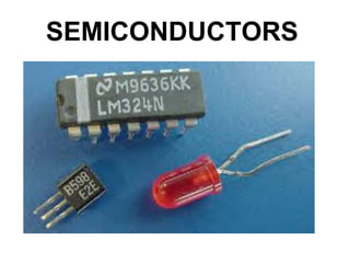
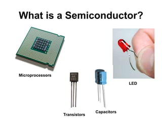
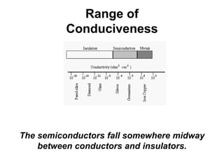
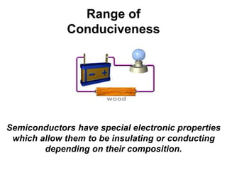
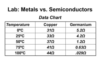
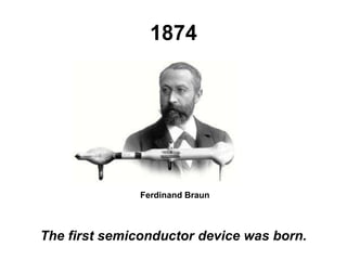
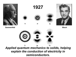
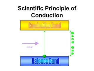
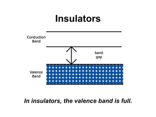
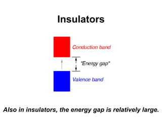
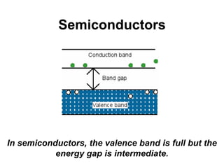
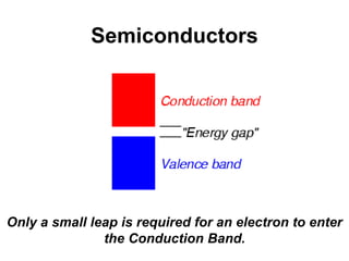
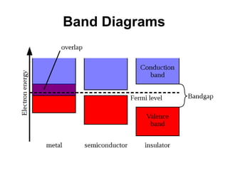
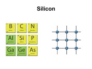
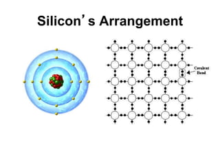
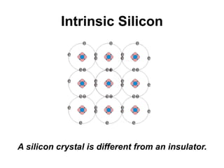
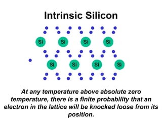
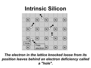
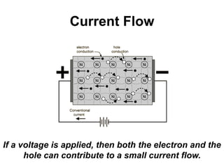
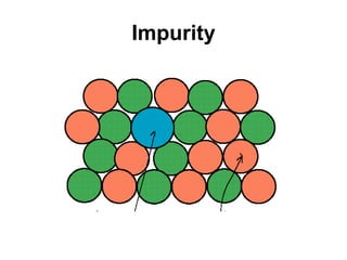
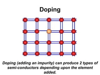
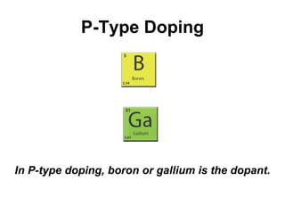
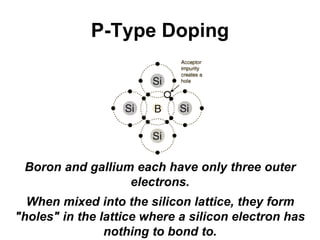
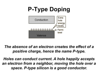
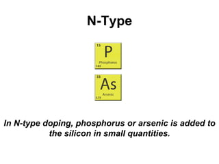
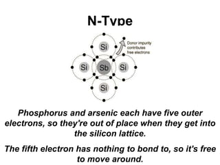
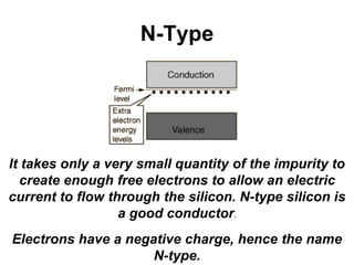
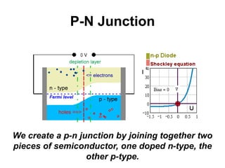
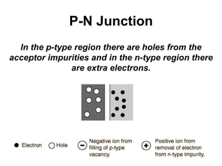
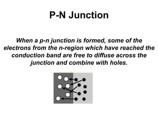
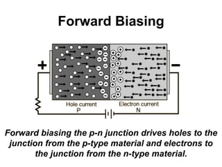
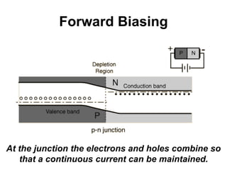
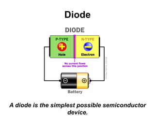
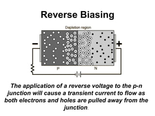
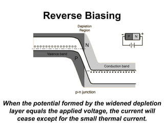
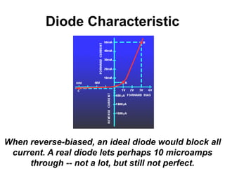
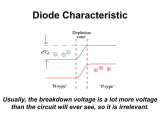
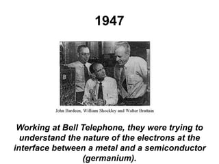
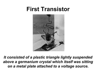
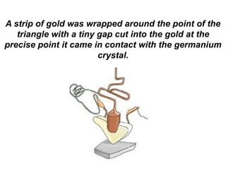
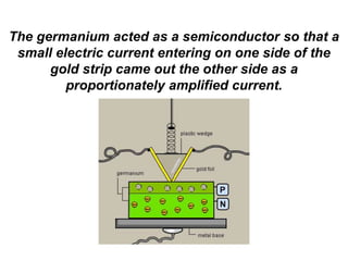
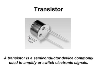
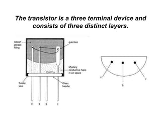
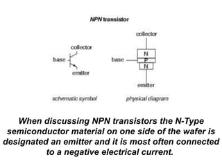
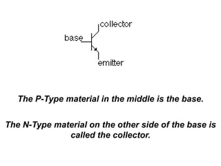
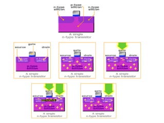
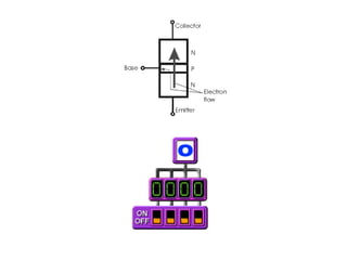
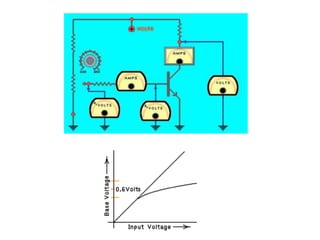
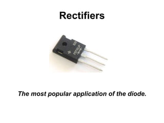
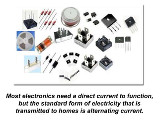
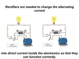
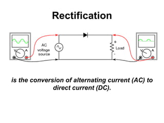
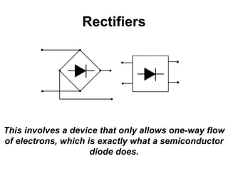
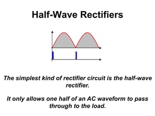
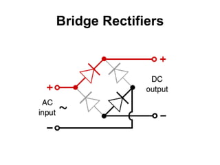
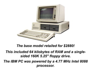
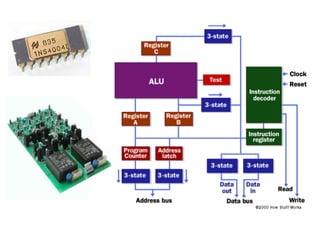
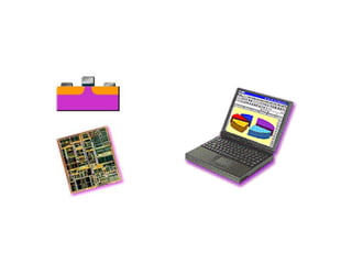
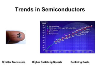
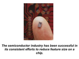
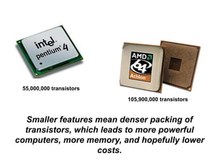
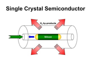
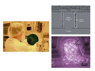
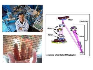
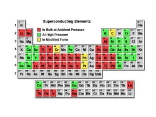
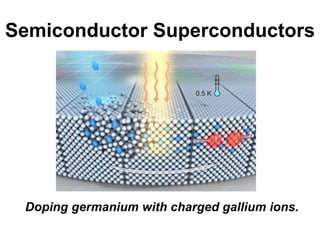
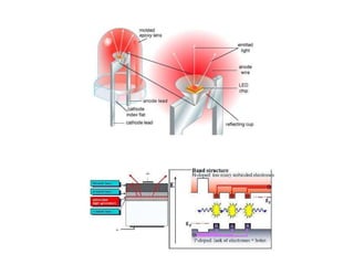
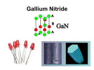
15. Radio receivers required a device called a rectifier to
detect signals.
He used the rectifying properties of the galena
crystal, a semiconductor material composed of lead
sulfide, to create the cat's whisker diode for this
purpose.
18. Valence Band
Most electrons remain bound to the atoms in this
band.
The highest occupied energy band is called the
valence band.
19. Conduction Band
The conduction band is the band of orbitals that are
high in energy and are generally empty.
It is the band that accepts the electrons from the
valence band.
20. Energy Gap
The “leap” required for electrons from the Valence
Band to enter the Conduction Band.
22. Conductors
In a conductor, electrons can move freely among
these orbitals within an energy band as long as the
orbitals are not completely occupied.
37. Intrinsic Silicon
At any temperature above absolute zero
temperature, there is a finite probability that an
electron in the lattice will be knocked loose from its
position.
38. Intrinsic Silicon
The electron in the lattice knocked loose from its
position leaves behind an electron deficiency called
a "hole".
39. Current Flow
If a voltage is applied, then both the electron and the
hole can contribute to a small current flow.
44. P-Type Doping
Boron and gallium each have only three outer
electrons.
When mixed into the silicon lattice, they form
"holes" in the lattice where a silicon electron has
nothing to bond to.
45. P-Type Doping
The absence of an electron creates the effect of a
positive charge, hence the name P-type.
Holes can conduct current. A hole happily accepts
an electron from a neighbor, moving the hole over a
space. P-type silicon is a good conductor.
48. N-Type
Phosphorus and arsenic each have five outer
electrons, so they're out of place when they get into
the silicon lattice.
The fifth electron has nothing to bond to, so it's free
to move around.
49. N-Type
It takes only a very small quantity of the impurity to
create enough free electrons to allow an electric
current to flow through the silicon. N-type silicon is
a good conductor.
Electrons have a negative charge, hence the name
N-type.
50. P-N Junction
We create a p-n junction by joining together two
pieces of semiconductor, one doped n-type, the
other p-type.
51. P-N Junction
In the n-type region there are extra electrons and in
the p-type region, there are holes from the acceptor
impurities .
52. P-N Junction
In the p-type region there are holes from the
acceptor impurities and in the n-type region there
are extra electrons.
53. P-N Junction
When a p-n junction is formed, some of the
electrons from the n-region which have reached the
conduction band are free to diffuse across the
junction and combine with holes.
54. P-N Junction
Filling a hole makes a negative ion and leaves
behind a positive ion on the n-side.
A space charge builds up, creating a depletion
region.
55. P-N Junction
This causes a depletion zone to form around the
junction (the join) between the two materials.
This zone controls the behavior of the diode.
56. Forward Biasing
Forward biasing the p-n junction drives holes to the
junction from the p-type material and electrons to
the junction from the n-type material.
57. Forward Biasing
At the junction the electrons and holes combine so
that a continuous current can be maintained.
59. One Way Electric “Turnstile”
A diode allows current to flow in one direction but
not the other.
60. Jumping
If you apply enough reverse voltage, the junction
breaks down and lets current through.
61. Reverse Biasing
The application of a reverse voltage to the p-n
junction will cause a transient current to flow as
both electrons and holes are pulled away from the
junction.
62. Reverse Biasing
When the potential formed by the widened depletion
layer equals the applied voltage, the current will
cease except for the small thermal current.
63. This voltage is needed to start the hole-electron
combination process at the junction.
When forward-biased, there is a small amount of
voltage necessary to get the diode going. In silicon,
this voltage is about 0.7 volts.
64. Diode Characteristic
When reverse-biased, an ideal diode would block all
current. A real diode lets perhaps 10 microamps
through -- not a lot, but still not perfect.
66. 1947
Working at Bell Telephone, they were trying to
understand the nature of the electrons at the
interface between a metal and a semiconductor
(germanium).
67. First Transistor
It consisted of a plastic triangle lightly suspended
above a germanium crystal which itself was sitting
on a metal plate attached to a voltage source.
68. A strip of gold was wrapped around the point of the
triangle with a tiny gap cut into the gold at the
precise point it came in contact with the germanium
crystal.
69. The germanium acted as a semiconductor so that a
small electric current entering on one side of the
gold strip came out the other side as a
proportionately amplified current.
71. Transistor
A transistor is a semiconductor device commonly
used to amplify or switch electronic signals.
72. The transistor is a three terminal device and
consists of three distinct layers.
73. Two of them are doped to give one type of
semiconductor and the there is the opposite type,
i.e. two may be n-type and one p-type, or two may be
p-type and one may be n-type.
They are designated either P-N-P (PNP) types of N-P-
N (NPN).
74. When discussing NPN transistors the N-Type
semiconductor material on one side of the wafer is
designated an emitter and it is most often connected
to a negative electrical current.
75. The P-Type material in the middle is the base.
The N-Type material on the other side of the base is
called the collector.
76.
77.
78. Highly automated manufacturing processes,
resulting in low per-unit cost.
Transistor Advantages
Extremely long life.
Higher reliability and greater physical ruggedness.
79. Small size and minimal weight, allowing the
development of miniaturized electronic devices.
Lower possible operating voltages, making
transistors suitable for small, battery-powered
applications.
86. Rectifiers
This involves a device that only allows one-way flow
of electrons, which is exactly what a semiconductor
diode does.
87. Half-Wave Rectifiers
The simplest kind of rectifier circuit is the half-wave
rectifier.
It only allows one half of an AC waveform to pass
through to the load.
88. Half-wave rectification is a very simple way to
reduce power to a resistive load.
Some two-position lamp dimmer switches apply full
AC power to the lamp filament for “full” brightness
and then half-wave rectify it for a lesser light output.
90. The invention of the transistor or semiconductor
was probably the most important development that
lead to the personal computers amazing growth and
what we know of as modern day computers.
91. 1959
The First I.C.
Jack Kilby at Texas Instruments and Robert Noyce
at Fairchild Camera, came up with a solution to the
problem of large numbers of components, and the
integrated circuit was developed.
92. Instead of making transistors one-by-one, several
transistors could be made at the same time, on the
same piece of semiconductor( a silicon wafer).
Not only transistors, but other electric components
such as resistors, capacitors and diodes could be
made by the same process with the same materials.
94. 1981
The IBM PC model 5150 was announced at a press
conference in New York on August 12, 1981 and
became available for purchase in early Fall 1981.
95. The base model retailed for $2880!
This included 64 kilobytes of RAM and a single-
sided 160K 5.25" floppy drive.
The IBM PC was powered by a 4.77 MHz Intel 8088
processor.