SlideShare a Scribd company logo
Basic Electronics (EEE-231)
Lecture 1
Instructor: Iqbal Ahmed Khurshid
Email: iqbal.ahmed.1@hotmail.com
Course Structure
• Credit Hours: 3
• Lectures: 30
• Quizzes: 4
• Assignments: 4
• Mid Exam: After 15 Lectures (25 marks)
• Final Exam of 50 marks
• Minimum 80% attendance (24 Lecs) required to sit in the final exam
Basic Electronics 3
Marks Division
• Quizzes 10%
• Assignments 10%
• Mid-Term Exam 30%
• Final Term Exam 50%
Basic Electronics 4
Basic Electronics
5
Course Outline
• Fundamentals of Semiconductor Physics: Band Theory, Intrinsic and
Extrinsic Semi-conductors
• P.N. Junction Diode, P.N. Junction as Rectifier
• Clipper and Clamper Circuits
• Zener Diode and Voltage Regulator, LED and LCD etc.
• Transistors, BJT Transistors, Biasing Techniques, Q Point Variations,
BJT as switch, BJT amplifiers
• Classes of amplifiers, Power amplifiers
• Metal oxide transistors, nMOS, pMOS, and CMOS Inverter circuits
• Introduction to A/D and D/A circuits
Basic Electronics 6
Required Literature
Book 1
Electronics Devices and Circuit Theory by Boylestad,
Eleventh Edition
Book 2
Electronic Devices by Thomas L. Floyd Ninth Edition
Basic Electronics 7
Prerequisite: DC Circuit analysis
Circuit analysis is the process of finding the voltages across, and the currents through, every
component in the circuit.
For dc circuits the components are resistive only and analysis is simpler.
Ohm Law,
Series, Parallel circuits,
Kirchhoff’s voltage and current laws,
Current, Voltage divider rules,
Thevenin, Norton’s theorems.
Basic Electronics 8
THE ATOM
• All matter is composed of atoms; all atoms consist of electrons,
protons, and neutrons except normal hydrogen, which does not have
a neutron.
• The atom is not a single particle but was made up of a small dense
nucleus around which electrons orbit at great distances from the
nucleus, similar to the way planets orbit the sun.
• The nucleus consists of positively charged particles called protons
and uncharged particles called neutrons. The basic particles of
negative charge are called electrons.
Basic Electronics 9
THE ATOM
• The atomic number equals the number of protons in the nucleus,
which is the same as the number of electrons in an electrically
balanced (neutral) atom.
Basic Electronics 10
Periodic Table
Basic Electronics 11
Electrons and Shells
• Electrons orbit the nucleus of an atom at certain distances from the
nucleus.
• Electrons near the nucleus have less energy than those in more
distant orbits.
• Each discrete distance (orbit) from the nucleus corresponds to a
certain energy level.
• In an atom, the orbits are grouped into energy levels known as shells.
• The shells (energy levels) are designated 1, 2, 3, and so on, with 1
being closest to the nucleus.
Basic Electronics 12
Electrons and Shells
Basic Electronics 13
Equation 1–1
• The Maximum Number of Electrons in Each Shell The
maximum number of electrons (Ne) that can exist in
each shell of an atom is a fact of nature and can be
calculated by the formula,
Basic Electronics 14
MATERIALS USED IN ELECTRONICS
• In terms of their electrical properties, materials can be classified into
three groups:
i. Conductors,
ii. Semiconductors
iii. Insulators
• An atom can be represented by the valence shell and a core that consists of
all the inner shells and the nucleus.
Basic Electronics 15
Insulators
• An insulator is a material that does not conduct electrical current
under normal conditions.
• Most good insulators are compounds rather than single-element
materials and have very high resistivities.
• Valence electrons are tightly bound to the atoms; therefore, there are
very few free electrons in an insulator.
• Examples of insulators are rubber, plastics, glass, mica, and quartz.
Basic Electronics 16
Conductors
• A conductor is a material that easily conducts electrical current.
• Most metals are good conductors. The best conductors are single-
element materials, such as copper (Cu), silver (Ag), gold (Au), and
aluminum (Al), which are characterized by atoms with only one
valence electron very loosely bound to the atom.
• These loosely bound valence electrons become free electrons.
Therefore, in a conductive material the free electrons are valence
electrons.
Basic Electronics 17
Semiconductors
• A semiconductor is a material that is between conductors
and insulators in its ability to conduct electrical current.
• A semiconductor in its pure (intrinsic) state is neither a good
conductor nor a good insulator.
• Single-element semiconductors are antimony (Sb), arsenic
(As), astatine (At), boron (B), polonium (Po), tellurium (Te),
silicon (Si), and germanium (Ge).
Basic Electronics 18
Band Gap
• Recall that the valence shell of an atom represents a band of energy levels and
that the valence electrons are confined to that band.
• When an electron acquires enough additional energy, it can leave the valence
shell, become a free electron, and exist in what is known as the conduction
band.
• The difference in energy between the valence band and the conduction band is
called an energy gap or band gap.
• This is the amount of energy that a valence electron must have in order to jump
from the valence band to the conduction band.
Basic Electronics 19
Band Gap
Basic Electronics 20
Band Gap
Basic Electronics 21
Band Gap
• The energy gap also reveals which elements are useful in the
construction of light-emitting devices such as light-emitting diodes
(LEDs), which will be introduced shortly.
• The wider the energy gap, the greater is the possibility of energy
being released in the form of visible or invisible (infrared) light waves.
• The unit of measure is appropriate because W (energy) = QV (as
derived from the defining equation for voltage: V = W / Q ).
• Substituting the charge of one electron and a potential difference of 1
V results in an energy level referred to as one electron volt .
Basic Electronics 22
Comparison of a Semiconductor Atom to a Conductor Atom
• Silicon is a semiconductor and copper is a conductor. Bohr diagrams
of the silicon atom and the copper atom are shown in Figure 1–8.
Basic Electronics 23
Silicon and Germanium
• The atomic structures of silicon and germanium are compared in
Figure 1–9.
• Silicon is used in diodes, transistors, integrated circuits, and other
semiconductor devices.
• Notice that both silicon and germanium have the characteristic four
valence electrons.
Basic Electronics 24
Atomic structure of (a) silicon; (b) germanium; and
(c) gallium and arsenic.
Basic Electronics 25
Covalent Bonds
• Figure shows how each silicon atom positions itself with four adjacent
silicon atoms to form a silicon crystal.
• This sharing of valence electrons produces the covalent bonds that
hold the atoms together
• Covalent bonding in an intrinsic silicon crystal is shown in Figure. An
intrinsic crystal is one that has no impurities.
Basic Electronics 26
Covalent Bonds
Basic Electronics 27
Conduction Electrons and Holes
• An intrinsic (pure) silicon crystal at room temperature has sufficient
heat (thermal) energy for some valence electrons to jump the gap
from the valence band into the conduction band, becoming free
electrons. Free electrons are also called conduction electrons.
Basic Electronics 28
Conduction Electrons and Holes
• When an electron jumps to the conduction band, a vacancy is left in
the valence band within the crystal.
• This vacancy is called a hole. For every electron raised to the
conduction band by external energy, there is one hole left in the
valence band, creating what is called an electron-hole pair.
• Recombination occurs when a conduction-band electron loses energy
and falls back into a hole in the valence band.
Basic Electronics 29
Conduction Electrons and Holes
Basic Electronics 30
Electron Current
• When a voltage is applied across a piece of intrinsic silicon, as shown
in Figure, the thermally generated free electrons in the conduction
band, which are free to move randomly in the crystal structure, are
now easily attracted toward the positive end.
• This movement of free electrons is one type of current in a semi
conductive material and is called electron current.
Basic Electronics
31
Hole Current
• Another type of current occurs in the valence band, where the holes
created by the free electrons exist.
• A valence electron can move into a nearby hole with little change in
its energy level, thus leaving another hole where it came from.
• Effectively the hole has moved from one place to another in the
crystal structure, as illustrated in Figure.
• Although current in the valence band is produced by valence
electrons, it is called hole current to distinguish it from electron
current in the conduction band.
Basic Electronics 32
Electron and Hole Current
Basic Electronics 33
N-TYPE AND P-TYPE SEMICONDUCTORS
• Semi conductive materials do not conduct current well and are of limited
value in their intrinsic state.
• This is because of the limited number of free electrons in the conduction
band and holes in the valence band.
• Intrinsic silicon (or germanium) must be modified by increasing the
number of free electrons or holes to increase its conductivity and make it
useful in electronic devices.
• This is done by adding impurities to the intrinsic material.
• Two types of extrinsic (impure) semi conductive materials, n-type and p-
type, are the key building blocks for most types of electronic devices.
Basic Electronics 34
N-Type Semiconductor
• To increase the number of conduction-band electrons in intrinsic silicon,
pentavalent impurity atoms are added. These are atoms with five valence
electrons such as arsenic (As), phosphorus (P), bismuth (Bi), and antimony
(Sb).
• As illustrated in Figure, each pentavalent atom (antimony, in this case)
forms covalent bonds with four adjacent silicon atoms.
• Four of the antimony atom’s valence electrons are used to form the
covalent bonds with silicon atoms, leaving one extra electron.
• This extra electron becomes a conduction electron because it is not
involved in bonding.
• Because the pentavalent atom gives up an electron, it is often called a
donor atom.
Basic Electronics 35
N-Type Semiconductor
Basic Electronics 36
Majority and Minority Carriers
• Since most of the current carriers are electrons, silicon (or
germanium) doped with pentavalent atoms is an n-type
semiconductor (the n stands for the negative charge on an electron).
• The electrons are called the majority carriers in n-type material.
Although the majority of current carriers in n-type material are
electrons, there are also a few holes that are created when electron-
hole pairs are thermally generated.
• These holes are not produced by the addition of the pentavalent
impurity atoms. Holes in an n-type material are called minority
carriers.
Basic Electronics 37
P-Type Semiconductor
• To increase the number of holes in intrinsic silicon, trivalent impurity
atoms are added.
• These are atoms with three valence electrons such as boron (B),
indium (In), and gallium (Ga).
• As illustrated in Figure, each trivalent atom (boron, in this case) forms
covalent bonds with four adjacent silicon atoms.
• All three of the boron atom’s valence electrons are used in the
covalent bonds; and, since four electrons are required, a hole results
when each trivalent atom is added. Because the trivalent atom can
take an electron, it is often referred to as an acceptor atom.
Basic Electronics 38
P-Type Semiconductor
Basic Electronics 39
Majority and Minority Carriers
• Since most of the current carriers are holes, silicon (or germanium)
doped with trivalent atoms is called a p-type semiconductor. The
holes are the majority carriers in p-type material.
• Although the majority of current carriers in p-type material are holes,
there are also a few conduction-band electrons that are created when
electron-hole pairs are thermally generated.
• These conduction-band electrons are not produced by the addition of
the trivalent impurity atoms.
• Conduction-band electrons in p-type material are the minority
carriers
Basic Electronics 40
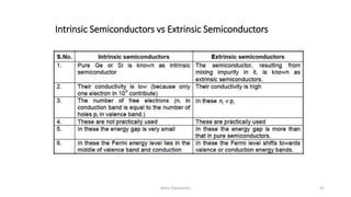
Intrinsic Semiconductors vs Extrinsic Semiconductors
Basic Electronics 41
THE PN JUNCTION
• When you take a block of silicon and dope part of it with a trivalent
impurity and the other part with a pentavalent impurity, a boundary
called the pn junction is formed between the resulting p-type and n-
type portions and a diode is created, as indicated in Figure.
• The pn junction is the basis for diodes, certain transistors, solar cells,
and other devices.
Basic Electronics 42
THE PN JUNCTION
Basic Electronics 43
Formation of the Depletion Region
• At the instant of the pn junction formation, the free electrons near
the junction in the n region begin to diffuse across the junction into
the p region where they combine with holes near the junction, as
shown in Figure.
• The term depletion refers to the fact that the region near the pn
junction is depleted of charge carriers (electrons and holes) due to
diffusion across the junction. Keep in mind that the depletion region
is formed very quickly and is very thin compared to the n region and
p region.
Basic Electronics 44
Barrier Potential
• The potential difference of the electric field across the depletion
region is the amount of voltage required to move electrons through
the electric field. This potential difference is called the barrier
potential and is expressed in volts.
Basic Electronics 45
The Diode
Basic Electronics 46
The Diode
Basic Electronics 47
No Applied Bias ( V = 0 V)
Basic Electronics 48
Reverse-Bias Condition ( V D < 0 V)
Basic Electronics 49
Reverse-Bias Condition ( V D < 0 V)
Basic Electronics 50
Forward-Bias Condition ( V D > 0 V)
Basic Electronics 51
Forward-Bias Condition ( V D > 0 V)
Basic Electronics 52
Characteristics of a semiconductor diode
• It can be demonstrated through the use of solid-state physics that the
general characteristics of a semiconductor diode can be defined by
the following equation, referred to as Shockley’s equation, for the
forward- and reverse-bias regions:
Basic Electronics 53
Basic Electronics 54
Silicon semiconductor diode characteristics.
Basic Electronics 55
Forward-bias
Basic Electronics 56
Basic Electronics 57

More Related Content

What's hot

Semiconductor materials
Semiconductor materialsSemiconductor materials
Semiconductor materials
SAIBHARGAV47
 
EEE231- Electronics-1 Lecture 01
EEE231- Electronics-1 Lecture 01EEE231- Electronics-1 Lecture 01
EEE231- Electronics-1 Lecture 01
rizwanspirit
 
Solids, Conductors, Insulators & Semiconductors
 Solids, Conductors, Insulators & Semiconductors Solids, Conductors, Insulators & Semiconductors
Solids, Conductors, Insulators & Semiconductors
KamalKhan822
 
Semiconductors
SemiconductorsSemiconductors
Semiconductors
SAURABH SINGH
 
Semiconductors materials
Semiconductors materialsSemiconductors materials
Semiconductors materials
abuamo
 
Lec1 introduction to semiconductors
Lec1 introduction to semiconductorsLec1 introduction to semiconductors
Lec1 introduction to semiconductors
Shakeel Akram
 
Introduction to Basic electronics
Introduction to Basic electronicsIntroduction to Basic electronics
Introduction to Basic electronics
Myrna Cabrera
 
Types of Semiconductor
Types of SemiconductorTypes of Semiconductor
Types of Semiconductor
HrshBhtgr
 
Ee2203 electronic-devices-and-circuits-lecture-notes
Ee2203 electronic-devices-and-circuits-lecture-notesEe2203 electronic-devices-and-circuits-lecture-notes
Ee2203 electronic-devices-and-circuits-lecture-notes
drmbalu
 
Semiconductors
SemiconductorsSemiconductors
Semiconductors
Rakesh Huike
 
Silicon in Semiconductor devices
Silicon in Semiconductor devices Silicon in Semiconductor devices
Silicon in Semiconductor devices
Ashish Singh
 
Solid state electronics
Solid state electronicsSolid state electronics
Solid state electronics
sultansaifuddin1
 
Semiconductor Diodes Engineering Circuit Analysis
Semiconductor Diodes Engineering Circuit AnalysisSemiconductor Diodes Engineering Circuit Analysis
Semiconductor Diodes Engineering Circuit Analysis
UMAR ALI
 
Conductor semiconductor insulator
Conductor semiconductor insulatorConductor semiconductor insulator
Conductor semiconductor insulator
ravikumar s
 
Semiconductor
SemiconductorSemiconductor
Semiconductor
T GOWTHAMAN
 
semiconductor - description and application
semiconductor - description and applicationsemiconductor - description and application
semiconductor - description and application
BishnupadaSarkar2
 
Semiconductor and it's types
Semiconductor and it's typesSemiconductor and it's types
Semiconductor and it's types
Arunkumar Arunkumar
 
Electrical conductivity
Electrical conductivityElectrical conductivity
Electrical conductivity
PBhaskar2
 
Engineering Physics - II second semester Anna University lecturer notes
Engineering Physics - II second semester Anna University lecturer notesEngineering Physics - II second semester Anna University lecturer notes
Engineering Physics - II second semester Anna University lecturer notes
24x7house
 
Semiconductors (rawat d agreatt)
Semiconductors (rawat d agreatt)Semiconductors (rawat d agreatt)
Semiconductors (rawat d agreatt)
Rawat DA Greatt
 

What's hot (20)

Semiconductor materials
Semiconductor materialsSemiconductor materials
Semiconductor materials
 
EEE231- Electronics-1 Lecture 01
EEE231- Electronics-1 Lecture 01EEE231- Electronics-1 Lecture 01
EEE231- Electronics-1 Lecture 01
 
Solids, Conductors, Insulators & Semiconductors
 Solids, Conductors, Insulators & Semiconductors Solids, Conductors, Insulators & Semiconductors
Solids, Conductors, Insulators & Semiconductors
 
Semiconductors
SemiconductorsSemiconductors
Semiconductors
 
Semiconductors materials
Semiconductors materialsSemiconductors materials
Semiconductors materials
 
Lec1 introduction to semiconductors
Lec1 introduction to semiconductorsLec1 introduction to semiconductors
Lec1 introduction to semiconductors
 
Introduction to Basic electronics
Introduction to Basic electronicsIntroduction to Basic electronics
Introduction to Basic electronics
 
Types of Semiconductor
Types of SemiconductorTypes of Semiconductor
Types of Semiconductor
 
Ee2203 electronic-devices-and-circuits-lecture-notes
Ee2203 electronic-devices-and-circuits-lecture-notesEe2203 electronic-devices-and-circuits-lecture-notes
Ee2203 electronic-devices-and-circuits-lecture-notes
 
Semiconductors
SemiconductorsSemiconductors
Semiconductors
 
Silicon in Semiconductor devices
Silicon in Semiconductor devices Silicon in Semiconductor devices
Silicon in Semiconductor devices
 
Solid state electronics
Solid state electronicsSolid state electronics
Solid state electronics
 
Semiconductor Diodes Engineering Circuit Analysis
Semiconductor Diodes Engineering Circuit AnalysisSemiconductor Diodes Engineering Circuit Analysis
Semiconductor Diodes Engineering Circuit Analysis
 
Conductor semiconductor insulator
Conductor semiconductor insulatorConductor semiconductor insulator
Conductor semiconductor insulator
 
Semiconductor
SemiconductorSemiconductor
Semiconductor
 
semiconductor - description and application
semiconductor - description and applicationsemiconductor - description and application
semiconductor - description and application
 
Semiconductor and it's types
Semiconductor and it's typesSemiconductor and it's types
Semiconductor and it's types
 
Electrical conductivity
Electrical conductivityElectrical conductivity
Electrical conductivity
 
Engineering Physics - II second semester Anna University lecturer notes
Engineering Physics - II second semester Anna University lecturer notesEngineering Physics - II second semester Anna University lecturer notes
Engineering Physics - II second semester Anna University lecturer notes
 
Semiconductors (rawat d agreatt)
Semiconductors (rawat d agreatt)Semiconductors (rawat d agreatt)
Semiconductors (rawat d agreatt)
 

Similar to Be lec 1

Lecture-01.pdf
Lecture-01.pdfLecture-01.pdf
Lecture-01.pdf
MonirMorshed3
 
Ch02Semiconductorpptx__2022_10_03_21_55_50.pptx
Ch02Semiconductorpptx__2022_10_03_21_55_50.pptxCh02Semiconductorpptx__2022_10_03_21_55_50.pptx
Ch02Semiconductorpptx__2022_10_03_21_55_50.pptx
puneet mathur
 
CHAPTER 4_SEMICONDUCTORS.pptx
CHAPTER 4_SEMICONDUCTORS.pptxCHAPTER 4_SEMICONDUCTORS.pptx
CHAPTER 4_SEMICONDUCTORS.pptx
Tesfahun Molla
 
Electronic devices chapter 1- 3 (m.sc physics)
Electronic devices chapter 1- 3 (m.sc physics)Electronic devices chapter 1- 3 (m.sc physics)
Electronic devices chapter 1- 3 (m.sc physics)
Ali Farooq
 
Introduction semi materials-rev7-22
Introduction semi materials-rev7-22Introduction semi materials-rev7-22
Introduction semi materials-rev7-22
Vajee ALi
 
Introduction to Semiconductors.ppt
Introduction to Semiconductors.pptIntroduction to Semiconductors.ppt
Introduction to Semiconductors.ppt
ChristianAceSolidum
 
Introduction_Semi_Materials-6-09-10.ppt
Introduction_Semi_Materials-6-09-10.pptIntroduction_Semi_Materials-6-09-10.ppt
Introduction_Semi_Materials-6-09-10.ppt
Anna336806
 
Introduction_Semi_Materials-6-09-10.ppt
Introduction_Semi_Materials-6-09-10.pptIntroduction_Semi_Materials-6-09-10.ppt
Introduction_Semi_Materials-6-09-10.ppt
RyanAnderson41811
 
Band Theory1234.pptx
Band Theory1234.pptxBand Theory1234.pptx
Band Theory1234.pptx
DileepC7
 
Semiconductors
SemiconductorsSemiconductors
Semiconductors
A B Shinde
 
Introduction to semiconductor materials
Introduction to semiconductor materialsIntroduction to semiconductor materials
Introduction to semiconductor materials
Dr. Ghanshyam Singh
 
Lecture 1_Electrical Engineering.pptx
Lecture 1_Electrical Engineering.pptxLecture 1_Electrical Engineering.pptx
Lecture 1_Electrical Engineering.pptx
IbrahimALsultan6
 
Lecture-1.pdf
Lecture-1.pdfLecture-1.pdf
Lecture-1.pdf
DrYOGENDRAKUMARAWAST
 
SPM Form 5 Physics - Electronics
SPM Form 5 Physics - ElectronicsSPM Form 5 Physics - Electronics
SPM Form 5 Physics - Electronics
Loo Carmen
 
1 semiconductor material
1 semiconductor material1 semiconductor material
1 semiconductor material
Lemon Sour
 
PHY SR SC M01 INTRO.pptx
PHY SR SC M01 INTRO.pptxPHY SR SC M01 INTRO.pptx
PHY SR SC M01 INTRO.pptx
WedgerRealme
 
Semiconductor Physics
Semiconductor PhysicsSemiconductor Physics
Semiconductor Physics
Shahzaib Mahesar
 
Introduction_Semi_Materials-6-09-10.ppt
Introduction_Semi_Materials-6-09-10.pptIntroduction_Semi_Materials-6-09-10.ppt
Introduction_Semi_Materials-6-09-10.ppt
VinothHari2
 
Phy 4240 lec (7)
Phy 4240 lec (7)Phy 4240 lec (7)
Phy 4240 lec (7)
Dr. Abeer Kamal
 
Chapter 1_Basic concepts_Alexander_V32_Nov 2020.ppt
Chapter 1_Basic concepts_Alexander_V32_Nov 2020.pptChapter 1_Basic concepts_Alexander_V32_Nov 2020.ppt
Chapter 1_Basic concepts_Alexander_V32_Nov 2020.ppt
MubashirKhan230965
 

Similar to Be lec 1 (20)

Lecture-01.pdf
Lecture-01.pdfLecture-01.pdf
Lecture-01.pdf
 
Ch02Semiconductorpptx__2022_10_03_21_55_50.pptx
Ch02Semiconductorpptx__2022_10_03_21_55_50.pptxCh02Semiconductorpptx__2022_10_03_21_55_50.pptx
Ch02Semiconductorpptx__2022_10_03_21_55_50.pptx
 
CHAPTER 4_SEMICONDUCTORS.pptx
CHAPTER 4_SEMICONDUCTORS.pptxCHAPTER 4_SEMICONDUCTORS.pptx
CHAPTER 4_SEMICONDUCTORS.pptx
 
Electronic devices chapter 1- 3 (m.sc physics)
Electronic devices chapter 1- 3 (m.sc physics)Electronic devices chapter 1- 3 (m.sc physics)
Electronic devices chapter 1- 3 (m.sc physics)
 
Introduction semi materials-rev7-22
Introduction semi materials-rev7-22Introduction semi materials-rev7-22
Introduction semi materials-rev7-22
 
Introduction to Semiconductors.ppt
Introduction to Semiconductors.pptIntroduction to Semiconductors.ppt
Introduction to Semiconductors.ppt
 
Introduction_Semi_Materials-6-09-10.ppt
Introduction_Semi_Materials-6-09-10.pptIntroduction_Semi_Materials-6-09-10.ppt
Introduction_Semi_Materials-6-09-10.ppt
 
Introduction_Semi_Materials-6-09-10.ppt
Introduction_Semi_Materials-6-09-10.pptIntroduction_Semi_Materials-6-09-10.ppt
Introduction_Semi_Materials-6-09-10.ppt
 
Band Theory1234.pptx
Band Theory1234.pptxBand Theory1234.pptx
Band Theory1234.pptx
 
Semiconductors
SemiconductorsSemiconductors
Semiconductors
 
Introduction to semiconductor materials
Introduction to semiconductor materialsIntroduction to semiconductor materials
Introduction to semiconductor materials
 
Lecture 1_Electrical Engineering.pptx
Lecture 1_Electrical Engineering.pptxLecture 1_Electrical Engineering.pptx
Lecture 1_Electrical Engineering.pptx
 
Lecture-1.pdf
Lecture-1.pdfLecture-1.pdf
Lecture-1.pdf
 
SPM Form 5 Physics - Electronics
SPM Form 5 Physics - ElectronicsSPM Form 5 Physics - Electronics
SPM Form 5 Physics - Electronics
 
1 semiconductor material
1 semiconductor material1 semiconductor material
1 semiconductor material
 
PHY SR SC M01 INTRO.pptx
PHY SR SC M01 INTRO.pptxPHY SR SC M01 INTRO.pptx
PHY SR SC M01 INTRO.pptx
 
Semiconductor Physics
Semiconductor PhysicsSemiconductor Physics
Semiconductor Physics
 
Introduction_Semi_Materials-6-09-10.ppt
Introduction_Semi_Materials-6-09-10.pptIntroduction_Semi_Materials-6-09-10.ppt
Introduction_Semi_Materials-6-09-10.ppt
 
Phy 4240 lec (7)
Phy 4240 lec (7)Phy 4240 lec (7)
Phy 4240 lec (7)
 
Chapter 1_Basic concepts_Alexander_V32_Nov 2020.ppt
Chapter 1_Basic concepts_Alexander_V32_Nov 2020.pptChapter 1_Basic concepts_Alexander_V32_Nov 2020.ppt
Chapter 1_Basic concepts_Alexander_V32_Nov 2020.ppt
 

Recently uploaded

132/33KV substation case study Presentation
132/33KV substation case study Presentation132/33KV substation case study Presentation
132/33KV substation case study Presentation
kandramariana6
 
Recycled Concrete Aggregate in Construction Part III
Recycled Concrete Aggregate in Construction Part IIIRecycled Concrete Aggregate in Construction Part III
Recycled Concrete Aggregate in Construction Part III
Aditya Rajan Patra
 
[JPP-1] - (JEE 3.0) - Kinematics 1D - 14th May..pdf
[JPP-1] - (JEE 3.0) - Kinematics 1D - 14th May..pdf[JPP-1] - (JEE 3.0) - Kinematics 1D - 14th May..pdf
[JPP-1] - (JEE 3.0) - Kinematics 1D - 14th May..pdf
awadeshbabu
 
DfMAy 2024 - key insights and contributions
DfMAy 2024 - key insights and contributionsDfMAy 2024 - key insights and contributions
DfMAy 2024 - key insights and contributions
gestioneergodomus
 
bank management system in java and mysql report1.pdf
bank management system in java and mysql report1.pdfbank management system in java and mysql report1.pdf
bank management system in java and mysql report1.pdf
Divyam548318
 
5214-1693458878915-Unit 6 2023 to 2024 academic year assignment (AutoRecovere...
5214-1693458878915-Unit 6 2023 to 2024 academic year assignment (AutoRecovere...5214-1693458878915-Unit 6 2023 to 2024 academic year assignment (AutoRecovere...
5214-1693458878915-Unit 6 2023 to 2024 academic year assignment (AutoRecovere...
ihlasbinance2003
 
Technical Drawings introduction to drawing of prisms
Technical Drawings introduction to drawing of prismsTechnical Drawings introduction to drawing of prisms
Technical Drawings introduction to drawing of prisms
heavyhaig
 
22CYT12-Unit-V-E Waste and its Management.ppt
22CYT12-Unit-V-E Waste and its Management.ppt22CYT12-Unit-V-E Waste and its Management.ppt
22CYT12-Unit-V-E Waste and its Management.ppt
KrishnaveniKrishnara1
 
Generative AI leverages algorithms to create various forms of content
Generative AI leverages algorithms to create various forms of contentGenerative AI leverages algorithms to create various forms of content
Generative AI leverages algorithms to create various forms of content
Hitesh Mohapatra
 
Advanced control scheme of doubly fed induction generator for wind turbine us...
Advanced control scheme of doubly fed induction generator for wind turbine us...Advanced control scheme of doubly fed induction generator for wind turbine us...
Advanced control scheme of doubly fed induction generator for wind turbine us...
IJECEIAES
 
2. Operations Strategy in a Global Environment.ppt
2. Operations Strategy in a Global Environment.ppt2. Operations Strategy in a Global Environment.ppt
2. Operations Strategy in a Global Environment.ppt
PuktoonEngr
 
Wearable antenna for antenna applications
Wearable antenna for antenna applicationsWearable antenna for antenna applications
Wearable antenna for antenna applications
Madhumitha Jayaram
 
RAT: Retrieval Augmented Thoughts Elicit Context-Aware Reasoning in Long-Hori...
RAT: Retrieval Augmented Thoughts Elicit Context-Aware Reasoning in Long-Hori...RAT: Retrieval Augmented Thoughts Elicit Context-Aware Reasoning in Long-Hori...
RAT: Retrieval Augmented Thoughts Elicit Context-Aware Reasoning in Long-Hori...
thanhdowork
 
IEEE Aerospace and Electronic Systems Society as a Graduate Student Member
IEEE Aerospace and Electronic Systems Society as a Graduate Student MemberIEEE Aerospace and Electronic Systems Society as a Graduate Student Member
IEEE Aerospace and Electronic Systems Society as a Graduate Student Member
VICTOR MAESTRE RAMIREZ
 
A review on techniques and modelling methodologies used for checking electrom...
A review on techniques and modelling methodologies used for checking electrom...A review on techniques and modelling methodologies used for checking electrom...
A review on techniques and modelling methodologies used for checking electrom...
nooriasukmaningtyas
 
Heat Resistant Concrete Presentation ppt
Heat Resistant Concrete Presentation pptHeat Resistant Concrete Presentation ppt
Heat Resistant Concrete Presentation ppt
mamunhossenbd75
 
6th International Conference on Machine Learning & Applications (CMLA 2024)
6th International Conference on Machine Learning & Applications (CMLA 2024)6th International Conference on Machine Learning & Applications (CMLA 2024)
6th International Conference on Machine Learning & Applications (CMLA 2024)
ClaraZara1
 
14 Template Contractual Notice - EOT Application
14 Template Contractual Notice - EOT Application14 Template Contractual Notice - EOT Application
14 Template Contractual Notice - EOT Application
SyedAbiiAzazi1
 
Exception Handling notes in java exception
Exception Handling notes in java exceptionException Handling notes in java exception
Exception Handling notes in java exception
Ratnakar Mikkili
 
Literature Review Basics and Understanding Reference Management.pptx
Literature Review Basics and Understanding Reference Management.pptxLiterature Review Basics and Understanding Reference Management.pptx
Literature Review Basics and Understanding Reference Management.pptx
Dr Ramhari Poudyal
 

Recently uploaded (20)

132/33KV substation case study Presentation
132/33KV substation case study Presentation132/33KV substation case study Presentation
132/33KV substation case study Presentation
 
Recycled Concrete Aggregate in Construction Part III
Recycled Concrete Aggregate in Construction Part IIIRecycled Concrete Aggregate in Construction Part III
Recycled Concrete Aggregate in Construction Part III
 
[JPP-1] - (JEE 3.0) - Kinematics 1D - 14th May..pdf
[JPP-1] - (JEE 3.0) - Kinematics 1D - 14th May..pdf[JPP-1] - (JEE 3.0) - Kinematics 1D - 14th May..pdf
[JPP-1] - (JEE 3.0) - Kinematics 1D - 14th May..pdf
 
DfMAy 2024 - key insights and contributions
DfMAy 2024 - key insights and contributionsDfMAy 2024 - key insights and contributions
DfMAy 2024 - key insights and contributions
 
bank management system in java and mysql report1.pdf
bank management system in java and mysql report1.pdfbank management system in java and mysql report1.pdf
bank management system in java and mysql report1.pdf
 
5214-1693458878915-Unit 6 2023 to 2024 academic year assignment (AutoRecovere...
5214-1693458878915-Unit 6 2023 to 2024 academic year assignment (AutoRecovere...5214-1693458878915-Unit 6 2023 to 2024 academic year assignment (AutoRecovere...
5214-1693458878915-Unit 6 2023 to 2024 academic year assignment (AutoRecovere...
 
Technical Drawings introduction to drawing of prisms
Technical Drawings introduction to drawing of prismsTechnical Drawings introduction to drawing of prisms
Technical Drawings introduction to drawing of prisms
 
22CYT12-Unit-V-E Waste and its Management.ppt
22CYT12-Unit-V-E Waste and its Management.ppt22CYT12-Unit-V-E Waste and its Management.ppt
22CYT12-Unit-V-E Waste and its Management.ppt
 
Generative AI leverages algorithms to create various forms of content
Generative AI leverages algorithms to create various forms of contentGenerative AI leverages algorithms to create various forms of content
Generative AI leverages algorithms to create various forms of content
 
Advanced control scheme of doubly fed induction generator for wind turbine us...
Advanced control scheme of doubly fed induction generator for wind turbine us...Advanced control scheme of doubly fed induction generator for wind turbine us...
Advanced control scheme of doubly fed induction generator for wind turbine us...
 
2. Operations Strategy in a Global Environment.ppt
2. Operations Strategy in a Global Environment.ppt2. Operations Strategy in a Global Environment.ppt
2. Operations Strategy in a Global Environment.ppt
 
Wearable antenna for antenna applications
Wearable antenna for antenna applicationsWearable antenna for antenna applications
Wearable antenna for antenna applications
 
RAT: Retrieval Augmented Thoughts Elicit Context-Aware Reasoning in Long-Hori...
RAT: Retrieval Augmented Thoughts Elicit Context-Aware Reasoning in Long-Hori...RAT: Retrieval Augmented Thoughts Elicit Context-Aware Reasoning in Long-Hori...
RAT: Retrieval Augmented Thoughts Elicit Context-Aware Reasoning in Long-Hori...
 
IEEE Aerospace and Electronic Systems Society as a Graduate Student Member
IEEE Aerospace and Electronic Systems Society as a Graduate Student MemberIEEE Aerospace and Electronic Systems Society as a Graduate Student Member
IEEE Aerospace and Electronic Systems Society as a Graduate Student Member
 
A review on techniques and modelling methodologies used for checking electrom...
A review on techniques and modelling methodologies used for checking electrom...A review on techniques and modelling methodologies used for checking electrom...
A review on techniques and modelling methodologies used for checking electrom...
 
Heat Resistant Concrete Presentation ppt
Heat Resistant Concrete Presentation pptHeat Resistant Concrete Presentation ppt
Heat Resistant Concrete Presentation ppt
 
6th International Conference on Machine Learning & Applications (CMLA 2024)
6th International Conference on Machine Learning & Applications (CMLA 2024)6th International Conference on Machine Learning & Applications (CMLA 2024)
6th International Conference on Machine Learning & Applications (CMLA 2024)
 
14 Template Contractual Notice - EOT Application
14 Template Contractual Notice - EOT Application14 Template Contractual Notice - EOT Application
14 Template Contractual Notice - EOT Application
 
Exception Handling notes in java exception
Exception Handling notes in java exceptionException Handling notes in java exception
Exception Handling notes in java exception
 
Literature Review Basics and Understanding Reference Management.pptx
Literature Review Basics and Understanding Reference Management.pptxLiterature Review Basics and Understanding Reference Management.pptx
Literature Review Basics and Understanding Reference Management.pptx
 

Be lec 1

  • 1.
  • 2. Basic Electronics (EEE-231) Lecture 1 Instructor: Iqbal Ahmed Khurshid Email: iqbal.ahmed.1@hotmail.com
  • 3. Course Structure • Credit Hours: 3 • Lectures: 30 • Quizzes: 4 • Assignments: 4 • Mid Exam: After 15 Lectures (25 marks) • Final Exam of 50 marks • Minimum 80% attendance (24 Lecs) required to sit in the final exam Basic Electronics 3
  • 4. Marks Division • Quizzes 10% • Assignments 10% • Mid-Term Exam 30% • Final Term Exam 50% Basic Electronics 4
  • 6. Course Outline • Fundamentals of Semiconductor Physics: Band Theory, Intrinsic and Extrinsic Semi-conductors • P.N. Junction Diode, P.N. Junction as Rectifier • Clipper and Clamper Circuits • Zener Diode and Voltage Regulator, LED and LCD etc. • Transistors, BJT Transistors, Biasing Techniques, Q Point Variations, BJT as switch, BJT amplifiers • Classes of amplifiers, Power amplifiers • Metal oxide transistors, nMOS, pMOS, and CMOS Inverter circuits • Introduction to A/D and D/A circuits Basic Electronics 6
  • 7. Required Literature Book 1 Electronics Devices and Circuit Theory by Boylestad, Eleventh Edition Book 2 Electronic Devices by Thomas L. Floyd Ninth Edition Basic Electronics 7
  • 8. Prerequisite: DC Circuit analysis Circuit analysis is the process of finding the voltages across, and the currents through, every component in the circuit. For dc circuits the components are resistive only and analysis is simpler. Ohm Law, Series, Parallel circuits, Kirchhoff’s voltage and current laws, Current, Voltage divider rules, Thevenin, Norton’s theorems. Basic Electronics 8
  • 9. THE ATOM • All matter is composed of atoms; all atoms consist of electrons, protons, and neutrons except normal hydrogen, which does not have a neutron. • The atom is not a single particle but was made up of a small dense nucleus around which electrons orbit at great distances from the nucleus, similar to the way planets orbit the sun. • The nucleus consists of positively charged particles called protons and uncharged particles called neutrons. The basic particles of negative charge are called electrons. Basic Electronics 9
  • 10. THE ATOM • The atomic number equals the number of protons in the nucleus, which is the same as the number of electrons in an electrically balanced (neutral) atom. Basic Electronics 10
  • 12. Electrons and Shells • Electrons orbit the nucleus of an atom at certain distances from the nucleus. • Electrons near the nucleus have less energy than those in more distant orbits. • Each discrete distance (orbit) from the nucleus corresponds to a certain energy level. • In an atom, the orbits are grouped into energy levels known as shells. • The shells (energy levels) are designated 1, 2, 3, and so on, with 1 being closest to the nucleus. Basic Electronics 12
  • 13. Electrons and Shells Basic Electronics 13
  • 14. Equation 1–1 • The Maximum Number of Electrons in Each Shell The maximum number of electrons (Ne) that can exist in each shell of an atom is a fact of nature and can be calculated by the formula, Basic Electronics 14
  • 15. MATERIALS USED IN ELECTRONICS • In terms of their electrical properties, materials can be classified into three groups: i. Conductors, ii. Semiconductors iii. Insulators • An atom can be represented by the valence shell and a core that consists of all the inner shells and the nucleus. Basic Electronics 15
  • 16. Insulators • An insulator is a material that does not conduct electrical current under normal conditions. • Most good insulators are compounds rather than single-element materials and have very high resistivities. • Valence electrons are tightly bound to the atoms; therefore, there are very few free electrons in an insulator. • Examples of insulators are rubber, plastics, glass, mica, and quartz. Basic Electronics 16
  • 17. Conductors • A conductor is a material that easily conducts electrical current. • Most metals are good conductors. The best conductors are single- element materials, such as copper (Cu), silver (Ag), gold (Au), and aluminum (Al), which are characterized by atoms with only one valence electron very loosely bound to the atom. • These loosely bound valence electrons become free electrons. Therefore, in a conductive material the free electrons are valence electrons. Basic Electronics 17
  • 18. Semiconductors • A semiconductor is a material that is between conductors and insulators in its ability to conduct electrical current. • A semiconductor in its pure (intrinsic) state is neither a good conductor nor a good insulator. • Single-element semiconductors are antimony (Sb), arsenic (As), astatine (At), boron (B), polonium (Po), tellurium (Te), silicon (Si), and germanium (Ge). Basic Electronics 18
  • 19. Band Gap • Recall that the valence shell of an atom represents a band of energy levels and that the valence electrons are confined to that band. • When an electron acquires enough additional energy, it can leave the valence shell, become a free electron, and exist in what is known as the conduction band. • The difference in energy between the valence band and the conduction band is called an energy gap or band gap. • This is the amount of energy that a valence electron must have in order to jump from the valence band to the conduction band. Basic Electronics 19
  • 22. Band Gap • The energy gap also reveals which elements are useful in the construction of light-emitting devices such as light-emitting diodes (LEDs), which will be introduced shortly. • The wider the energy gap, the greater is the possibility of energy being released in the form of visible or invisible (infrared) light waves. • The unit of measure is appropriate because W (energy) = QV (as derived from the defining equation for voltage: V = W / Q ). • Substituting the charge of one electron and a potential difference of 1 V results in an energy level referred to as one electron volt . Basic Electronics 22
  • 23. Comparison of a Semiconductor Atom to a Conductor Atom • Silicon is a semiconductor and copper is a conductor. Bohr diagrams of the silicon atom and the copper atom are shown in Figure 1–8. Basic Electronics 23
  • 24. Silicon and Germanium • The atomic structures of silicon and germanium are compared in Figure 1–9. • Silicon is used in diodes, transistors, integrated circuits, and other semiconductor devices. • Notice that both silicon and germanium have the characteristic four valence electrons. Basic Electronics 24
  • 25. Atomic structure of (a) silicon; (b) germanium; and (c) gallium and arsenic. Basic Electronics 25
  • 26. Covalent Bonds • Figure shows how each silicon atom positions itself with four adjacent silicon atoms to form a silicon crystal. • This sharing of valence electrons produces the covalent bonds that hold the atoms together • Covalent bonding in an intrinsic silicon crystal is shown in Figure. An intrinsic crystal is one that has no impurities. Basic Electronics 26
  • 28. Conduction Electrons and Holes • An intrinsic (pure) silicon crystal at room temperature has sufficient heat (thermal) energy for some valence electrons to jump the gap from the valence band into the conduction band, becoming free electrons. Free electrons are also called conduction electrons. Basic Electronics 28
  • 29. Conduction Electrons and Holes • When an electron jumps to the conduction band, a vacancy is left in the valence band within the crystal. • This vacancy is called a hole. For every electron raised to the conduction band by external energy, there is one hole left in the valence band, creating what is called an electron-hole pair. • Recombination occurs when a conduction-band electron loses energy and falls back into a hole in the valence band. Basic Electronics 29
  • 30. Conduction Electrons and Holes Basic Electronics 30
  • 31. Electron Current • When a voltage is applied across a piece of intrinsic silicon, as shown in Figure, the thermally generated free electrons in the conduction band, which are free to move randomly in the crystal structure, are now easily attracted toward the positive end. • This movement of free electrons is one type of current in a semi conductive material and is called electron current. Basic Electronics 31
  • 32. Hole Current • Another type of current occurs in the valence band, where the holes created by the free electrons exist. • A valence electron can move into a nearby hole with little change in its energy level, thus leaving another hole where it came from. • Effectively the hole has moved from one place to another in the crystal structure, as illustrated in Figure. • Although current in the valence band is produced by valence electrons, it is called hole current to distinguish it from electron current in the conduction band. Basic Electronics 32
  • 33. Electron and Hole Current Basic Electronics 33
  • 34. N-TYPE AND P-TYPE SEMICONDUCTORS • Semi conductive materials do not conduct current well and are of limited value in their intrinsic state. • This is because of the limited number of free electrons in the conduction band and holes in the valence band. • Intrinsic silicon (or germanium) must be modified by increasing the number of free electrons or holes to increase its conductivity and make it useful in electronic devices. • This is done by adding impurities to the intrinsic material. • Two types of extrinsic (impure) semi conductive materials, n-type and p- type, are the key building blocks for most types of electronic devices. Basic Electronics 34
  • 35. N-Type Semiconductor • To increase the number of conduction-band electrons in intrinsic silicon, pentavalent impurity atoms are added. These are atoms with five valence electrons such as arsenic (As), phosphorus (P), bismuth (Bi), and antimony (Sb). • As illustrated in Figure, each pentavalent atom (antimony, in this case) forms covalent bonds with four adjacent silicon atoms. • Four of the antimony atom’s valence electrons are used to form the covalent bonds with silicon atoms, leaving one extra electron. • This extra electron becomes a conduction electron because it is not involved in bonding. • Because the pentavalent atom gives up an electron, it is often called a donor atom. Basic Electronics 35
  • 37. Majority and Minority Carriers • Since most of the current carriers are electrons, silicon (or germanium) doped with pentavalent atoms is an n-type semiconductor (the n stands for the negative charge on an electron). • The electrons are called the majority carriers in n-type material. Although the majority of current carriers in n-type material are electrons, there are also a few holes that are created when electron- hole pairs are thermally generated. • These holes are not produced by the addition of the pentavalent impurity atoms. Holes in an n-type material are called minority carriers. Basic Electronics 37
  • 38. P-Type Semiconductor • To increase the number of holes in intrinsic silicon, trivalent impurity atoms are added. • These are atoms with three valence electrons such as boron (B), indium (In), and gallium (Ga). • As illustrated in Figure, each trivalent atom (boron, in this case) forms covalent bonds with four adjacent silicon atoms. • All three of the boron atom’s valence electrons are used in the covalent bonds; and, since four electrons are required, a hole results when each trivalent atom is added. Because the trivalent atom can take an electron, it is often referred to as an acceptor atom. Basic Electronics 38
  • 40. Majority and Minority Carriers • Since most of the current carriers are holes, silicon (or germanium) doped with trivalent atoms is called a p-type semiconductor. The holes are the majority carriers in p-type material. • Although the majority of current carriers in p-type material are holes, there are also a few conduction-band electrons that are created when electron-hole pairs are thermally generated. • These conduction-band electrons are not produced by the addition of the trivalent impurity atoms. • Conduction-band electrons in p-type material are the minority carriers Basic Electronics 40
  • 41. Intrinsic Semiconductors vs Extrinsic Semiconductors Basic Electronics 41
  • 42. THE PN JUNCTION • When you take a block of silicon and dope part of it with a trivalent impurity and the other part with a pentavalent impurity, a boundary called the pn junction is formed between the resulting p-type and n- type portions and a diode is created, as indicated in Figure. • The pn junction is the basis for diodes, certain transistors, solar cells, and other devices. Basic Electronics 42
  • 43. THE PN JUNCTION Basic Electronics 43
  • 44. Formation of the Depletion Region • At the instant of the pn junction formation, the free electrons near the junction in the n region begin to diffuse across the junction into the p region where they combine with holes near the junction, as shown in Figure. • The term depletion refers to the fact that the region near the pn junction is depleted of charge carriers (electrons and holes) due to diffusion across the junction. Keep in mind that the depletion region is formed very quickly and is very thin compared to the n region and p region. Basic Electronics 44
  • 45. Barrier Potential • The potential difference of the electric field across the depletion region is the amount of voltage required to move electrons through the electric field. This potential difference is called the barrier potential and is expressed in volts. Basic Electronics 45
  • 48. No Applied Bias ( V = 0 V) Basic Electronics 48
  • 49. Reverse-Bias Condition ( V D < 0 V) Basic Electronics 49
  • 50. Reverse-Bias Condition ( V D < 0 V) Basic Electronics 50
  • 51. Forward-Bias Condition ( V D > 0 V) Basic Electronics 51
  • 52. Forward-Bias Condition ( V D > 0 V) Basic Electronics 52
  • 53. Characteristics of a semiconductor diode • It can be demonstrated through the use of solid-state physics that the general characteristics of a semiconductor diode can be defined by the following equation, referred to as Shockley’s equation, for the forward- and reverse-bias regions: Basic Electronics 53
  • 55. Silicon semiconductor diode characteristics. Basic Electronics 55

Editor's Notes

  1. Dffs