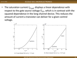
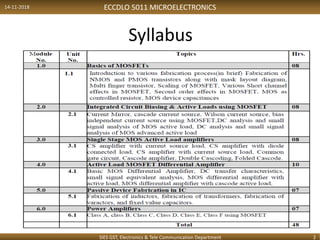
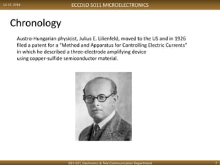
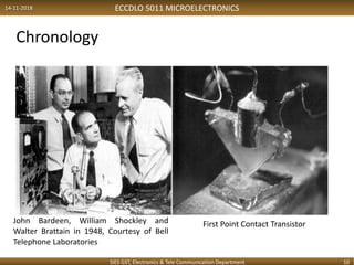
SlideShare a Scribd company logo
1 of 88
ECCDLO 5011 MICROELECTRONICS
ECCDLO 5011
Microelectronics
BY
Prof. Abhishek Ajit Kadam
Email id: kadam.abhishek@siesgst.ac.in
Mob No: 9730032260
14-11-2018
SIES GST, Electronics & Tele Communication Department 1
ECCDLO 5011 MICROELECTRONICS
Syllabus
14-11-2018
SIES GST, Electronics & Tele Communication Department 2
ECCDLO 5011 MICROELECTRONICS
Course Outcome
1. Define basic fabrication process of MOS Transistors.
2. Analyse MOS characteristics and Second order
effects in MOS Transistors.
3. Understand Integrated circuit biasing using MOSFET.
4. Design and implement active load MOS amplifier.
5. Design and implement active load differential
amplifier
6. To understand implementation of passive
components in ICs.
14-11-2018
SIES GST, Electronics & Tele Communication Department 3
ECCDLO 5011 MICROELECTRONICS
Text Books
• A. Sedra, K. Smith, adapted by A. Chandorkar “Microelectronic
Circuits-Theory and Application”
• D. Neamen, “Electronic Circuits Analysis and Design” , McGraw Hill
Education, 3rd Edition
• B. Razavi, “Design of Analog Integrated Circuits”, McGraw Hill
Education, Indian Edition
• ***B. Razavi, “Microelectronics”, Wiley India
• B. Razavi, “R F Microelectronics”, Pearson Publication, 2nd Edition
14-11-2018
SIES GST, Electronics & Tele Communication Department 4
ECCDLO 5011 MICROELECTRONICS14-11-2018
SIES GST, Electronics & Tele Communication Department 5
ECCDLO 5011 MICROELECTRONICS14-11-2018
SIES GST, Electronics & Tele Communication Department 6
ECCDLO 5011 MICROELECTRONICS14-11-2018
SIES GST, Electronics & Tele Communication Department 7
Chronology
Austro-Hungarian physicist, Julius E. Lilienfeld, moved to the US and in 1926
filed a patent for a “Method and Apparatus for Controlling Electric Currents”
in which he described a three-electrode amplifying device
using copper-sulfide semiconductor material.
ECCDLO 5011 MICROELECTRONICS14-11-2018
SIES GST, Electronics & Tele Communication Department 8
ECCDLO 5011 MICROELECTRONICS14-11-2018
SIES GST, Electronics & Tele Communication Department 9
• Because of their poor reliability and large power consumption, by the late 1930’s engineers at
American Telephone and Telegraph knew that vacuum-tube circuits would not meet the
company’s rapidly growing demand for increased phone call capacity.
• Using improved semiconductor materials developed for radar detectors during the war, in early
1945 Shockley experimented with a field-effect amplifier, similar in concept to those patented
by Heil and Lilienfeld, but it failed to work as he intended.
• Physicist John Bardeen suggested that electrons on the semiconductor surface might be
blocking penetration of electric fields into the material.
• Under Shockley’s direction, together with physicist Walter Brattain, Bardeen began researching
the behavior of these “surface states.”
• On December 16, 1947, their research culminated in a successful semiconductor amplifier.
Bardeen and Brattain applied two closely-spaced gold contacts held in place by a plastic wedge
to the surface of a small slab of high-purity germanium. On December 23 they demonstrated
their device to lab officials and in June 1948, Bell Labs publicly announced the revolutionary
solid-state device they called a “transistor.”
• Realizing that the point-contact structure had serious limitations, and spurred by professional
jealousy as he resented not being involved with its discovery, Shockley worked alone to
conceive a more reliable and reproducible device. Introduced in 1952, Shockley’s bipolar
junction transistor, which was made from a solid piece of semiconductor material and no point
contacts, dominated the industry for the next 30 years.
Chronology
ECCDLO 5011 MICROELECTRONICS14-11-2018
SIES GST, Electronics & Tele Communication Department 10
Chronology
John Bardeen, William Shockley and
Walter Brattain in 1948, Courtesy of Bell
Telephone Laboratories
First Point Contact Transistor
ECCDLO 5011 MICROELECTRONICS14-11-2018
SIES GST, Electronics & Tele Communication Department 11
Chronology
The ideas of Lilienfeld and Heil and Shockley’s failed early experiments finally bore fruit
in 1959 when, working for Egyptian engineer Martin M. (John) Atalla on the study of
semiconductor surfaces at Bell Labs, Korean electrical engineer Dawon Kahng built
the first successful field-effect transistor (FET) comprising a sandwich of layers of
metal (M – gate), oxide (O – insulation), and silicon (S – semiconductor).
Martin M. Atalla (1924 – 2009),
Courtesy of the Atalla Family
Dawon Kahng (1931 – 1992),
Courtesy NEC Corporation
ECCDLO 5011 MICROELECTRONICS14-11-2018
SIES GST, Electronics & Tele Communication Department 12
Voltage
ECCDLO 5011 MICROELECTRONICS14-11-2018
SIES GST, Electronics & Tele Communication Department 13
ECCDLO 5011 MICROELECTRONICS14-11-2018
SIES GST, Electronics & Tele Communication Department 14
ECCDLO 5011 MICROELECTRONICS
Moor’s Law
14-11-2018
SIES GST, Electronics & Tele Communication Department 15
ECCDLO 5011 MICROELECTRONICS14-11-2018
SIES GST, Electronics & Tele Communication Department 16
ECCDLO 5011 MICROELECTRONICS14-11-2018
SIES GST, Electronics & Tele Communication Department 17
ECCDLO 5011 MICROELECTRONICS14-11-2018
SIES GST, Electronics & Tele Communication Department 18
ECCDLO 5011 MICROELECTRONICS14-11-2018
SIES GST, Electronics & Tele Communication Department 19
ECCDLO 5011 MICROELECTRONICS14-11-2018
SIES GST, Electronics & Tele Communication Department 20
ECCDLO 5011 MICROELECTRONICS14-11-2018
SIES GST, Electronics & Tele Communication Department 21
ECCDLO 5011 MICROELECTRONICS14-11-2018
SIES GST, Electronics & Tele Communication Department 22
ECCDLO 5011 MICROELECTRONICS14-11-2018
SIES GST, Electronics & Tele Communication Department 23
7)
ECCDLO 5011 MICROELECTRONICS
Chapter 1
Basics of MOSFETs
14-11-2018
SIES GST, Electronics & Tele Communication Department 24
ECCDLO 5011 MICROELECTRONICS
• Physics Of Semiconductor Devices (A review)
𝑁(𝐸) is Density of states
𝐹(𝐸) is Fermi Dirac Probability Function
𝑛𝑖 𝑎𝑛𝑑 𝑝𝑖 are intrinsic Carrier Concentration
𝑛 = 𝑁𝑐 𝐸 . 𝐹 𝐸 𝑑𝐸 𝑝 = 𝑁𝑣 𝐸 . 1 − 𝐹 𝐸 𝑑𝐸
14-11-2018
SIES GST, Electronics & Tele Communication Department 25
ECCDLO 5011 MICROELECTRONICS
• Physics Of Semiconductor Devices (A review)
𝑁(𝐸) is Density of states
𝐹(𝐸) is Fermi Dirac Probability Function
𝑛𝑖 𝑎𝑛𝑑 𝑝𝑖 are intrinsic Carrier Concentration
𝑛 = 𝑁𝑐 𝐸 . 𝐹 𝐸 𝑑𝐸 𝑝 = 𝑁𝑣 𝐸 . 1 − 𝐹 𝐸 𝑑𝐸
Insertion of Donor Impurity like Prosperous (P) or Arsenic (As)
14-11-2018
SIES GST, Electronics & Tele Communication Department 26
ECCDLO 5011 MICROELECTRONICS
• Physics Of Semiconductor Devices (A review)
𝑁(𝐸) is Density of states
𝐹(𝐸) is Fermi Dirac Probability Function
𝑛𝑖 𝑎𝑛𝑑 𝑝𝑖 are intrinsic Carrier Concentration
𝑛 = 𝑁𝑐 𝐸 . 𝐹 𝐸 𝑑𝐸 𝑝 = 𝑁𝑣 𝐸 . 1 − 𝐹 𝐸 𝑑𝐸
Insertion of Donor Impurity like Boron(B), Aluminium(Al) or Gallium (Ga)
14-11-2018
SIES GST, Electronics & Tele Communication Department 27
ECCDLO 5011 MICROELECTRONICS
• P-N Junction
𝜓 𝑏𝑖 is Built in potential 0.7 V in Si
𝜙 𝑛 =
𝑘𝑇
𝑞
ln(𝑁 𝐷/𝑛𝑖) is difference
between 𝐸 𝐹 𝑎𝑛𝑑 𝐸𝑐
𝜙 𝑝 =
𝑘𝑇
𝑞
ln(𝑁𝐴/𝑛𝑖) is difference
between 𝐸 𝐹 𝑎𝑛𝑑 𝐸 𝑣
14-11-2018
SIES GST, Electronics & Tele Communication Department 28
ECCDLO 5011 MICROELECTRONICS
• Energy Band Diagram of Ideal MIS structure (n type)
14-11-2018
SIES GST, Electronics & Tele Communication Department 29
ECCDLO 5011 MICROELECTRONICS
• Energy Band Diagram of Ideal MIS structure (P type)
14-11-2018
SIES GST, Electronics & Tele Communication Department 30
ECCDLO 5011 MICROELECTRONICS
Basic Building Block “MOSFET”
14-11-2018
SIES GST, Electronics & Tele Communication Department 31
ECCDLO 5011 MICROELECTRONICS
Symbol
14-11-2018
SIES GST, Electronics & Tele Communication Department 32
ECCDLO 5011 MICROELECTRONICS14-11-2018
SIES GST, Electronics & Tele Communication Department 33
ECCDLO 5011 MICROELECTRONICS14-11-2018
SIES GST, Electronics & Tele Communication Department 34
MOSFET with gate voltage
formation of depletion region, formation of channel.
ECCDLO 5011 MICROELECTRONICS
• Threshold Voltage
The semiconductor/oxide surface is inverted when VGS is greater than the
Threshold voltage (VTH). The threshold voltage VTH is given by
𝑉𝑇 = 𝑉𝑇𝐻0 + 𝛾( 2𝜙 𝐹 + 𝑉𝑆𝐵 − |2𝜙 𝐹|)
Where 𝑉𝑇𝐻0 = 𝜙 𝑀𝑆 + 2𝜙 𝐹 +
𝑄 𝑑𝑒𝑝
𝐶 𝑜𝑥
Where 𝜙 𝑀𝑆 is difference between work function of polysillicon gate and
substrate. It is given by
𝜙 𝐹 =
𝑘𝑇
𝑞
ln[
𝑁𝑠𝑢𝑏
𝑛𝑖
]
Where
𝑞 is charge on electron given by 𝑒 = 1.6 ∗ 10−19
𝑐𝑜𝑢𝑙𝑜𝑚𝑏𝑠
𝑁𝑠𝑢𝑏 is doping concentration
𝑄 𝑑𝑒𝑝 is Depletion region charge given by (4𝑒𝜖 𝑠𝑖 𝜙 𝐹 𝑁𝑠𝑢𝑏)
𝐶 𝑜𝑥 is oxide capacitance per unit area given by
𝜖 𝑠𝑖
𝑡 𝑜𝑥
𝛾 is called as Body coefficient given by
2𝑒𝜖 𝑠𝑖 𝑁 𝑠𝑢𝑏
𝐶 𝑜𝑥
14-11-2018
SIES GST, Electronics & Tele Communication Department 35
ECCDLO 5011 MICROELECTRONICS14-11-2018
SIES GST, Electronics & Tele Communication Department 36
𝐼 𝐷 − 𝑉𝐺 𝑎𝑛𝑑 𝐼 𝐷 − 𝑉𝐷 𝑐ℎ𝑎𝑟𝑎𝑐𝑡𝑒𝑟𝑖𝑠𝑡𝑖𝑐𝑠 𝑓𝑜𝑟 𝑐ℎ𝑎𝑛𝑔𝑒 𝑖𝑛 𝐿𝑒𝑛𝑔𝑡ℎ
𝐼 𝐷 − 𝑉𝐺 𝑎𝑛𝑑 𝐼 𝐷 − 𝑉𝐷 𝑐ℎ𝑎𝑟𝑎𝑐𝑡𝑒𝑟𝑖𝑠𝑡𝑖𝑐𝑠 𝑓𝑜𝑟 𝑐ℎ𝑎𝑛𝑔𝑒 𝑖𝑛 𝑜𝑥𝑖𝑑𝑒 𝑇ℎ𝑖𝑐𝑘𝑛𝑒𝑠𝑠
ECCDLO 5011 MICROELECTRONICS14-11-2018
SIES GST, Electronics & Tele Communication Department 37
ECCDLO 5011 MICROELECTRONICS14-11-2018
SIES GST, Electronics & Tele Communication Department 38
ECCDLO 5011 MICROELECTRONICS14-11-2018
SIES GST, Electronics & Tele Communication Department 39
Derivation of I/V characteristics
ECCDLO 5011 MICROELECTRONICS14-11-2018
SIES GST, Electronics & Tele Communication Department 40
𝐼 𝑑 𝑣𝑠 𝑉𝑑𝑠 𝑐𝑢𝑟𝑣𝑒
ECCDLO 5011 MICROELECTRONICS14-11-2018
SIES GST, Electronics & Tele Communication Department 41
Transistor operating in Deep Triode region 𝑉𝐷𝑆 ≪ (𝑉𝐺𝑆 − 𝑉𝑇)
ECCDLO 5011 MICROELECTRONICS14-11-2018
SIES GST, Electronics & Tele Communication Department 42
ECCDLO 5011 MICROELECTRONICS14-11-2018
SIES GST, Electronics & Tele Communication Department 43
Pinch off Behaviour
ECCDLO 5011 MICROELECTRONICS14-11-2018
SIES GST, Electronics & Tele Communication Department 44
ECCDLO 5011 MICROELECTRONICS14-11-2018
SIES GST, Electronics & Tele Communication Department 45
Find the region of operation if 𝑉𝑇 = 0.4V
ECCDLO 5011 MICROELECTRONICS
MOS I-V Characteristics summery
SIES GST, Electronics & Tele Communication Department
• Triode Region
• Deep Triode Region
VDS ≪ 2(VGS − VT)
𝑅 𝑜𝑛 = 1/(𝜇 𝑛 𝐶 𝑜𝑥
𝑊
𝐿
𝑉𝐺𝑆 − 𝑉𝑇)
14-11-2018
46
ECCDLO 5011 MICROELECTRONICS
MOS I-V Characteristics summery
SIES GST, Electronics & Tele Communication Department
•Saturation Region
When pinch off condition occurs
Further when device enters in Saturation region where Drain
current is given by
𝐼 𝐷 =
𝜇 𝑛 𝐶 𝑜𝑥
𝑊
𝐿
2
𝑉𝐺𝑆 − 𝑉𝑇
2
𝐼 𝐷 =
𝛽 𝑛
2
𝑉𝐺𝑆 − 𝑉𝑇
2 𝑎𝑛𝑑 𝑅 𝑜𝑛 = ∞
14-11-2018
47
ECCDLO 5011 MICROELECTRONICS
Transconductance
SIES GST, Electronics & Tele Communication Department
Transconductance is defined as ratio of change in Id and Vgs
𝑔 𝑚 =
𝛿 𝐼 𝐷
𝛿(𝑉𝐺𝑆)
Where is referred as overdrive voltage
14-11-2018
48
ECCDLO 5011 MICROELECTRONICS14-11-2018
SIES GST, Electronics & Tele Communication Department 49
• MOS Transconductance as function of 𝑉𝑜𝑣 & 𝐼 𝐷
ECCDLO 5011 MICROELECTRONICS
MOSFET SCALING
14-11-2018
SIES GST, Electronics & Tele Communication Department 50
ECCDLO 5011 MICROELECTRONICS14-11-2018
SIES GST, Electronics & Tele Communication Department 51
Moors Law
ECCDLO 5011 MICROELECTRONICS14-11-2018
SIES GST, Electronics & Tele Communication Department 52
ECCDLO 5011 MICROELECTRONICS
Types of scaling
• Constant Field Scaling or Full scaling
• Constant Voltage Scaling
14-11-2018
SIES GST, Electronics & Tele Communication Department 53
ECCDLO 5011 MICROELECTRONICS
Constant Field Scaling
• Magnitude of internal electric fields is kept
constant.
• Only lateral dimensions are changed.
• Threshold voltage is also effected.
14-11-2018
SIES GST, Electronics & Tele Communication Department 54
ECCDLO 5011 MICROELECTRONICS
Consequences of Constant Field Scaling
14-11-2018
SIES GST, Electronics & Tele Communication Department 55
ECCDLO 5011 MICROELECTRONICS
Consequences of Constant Field Scaling
14-11-2018
SIES GST, Electronics & Tele Communication Department 56
• Most significant reduction :
– Power dissipation is reduced by a factor of S² as P´= P/S²
– Power density remains unchanged.
– Gate oxide capacitance is scaled down as Cg´ = Cg/S
– Overall performance improvement.
ECCDLO 5011 MICROELECTRONICS
Constant Voltage Scaling :
• More preferred.
• All dimensions are scaled down except power supply
and terminal voltages.
14-11-2018
SIES GST, Electronics & Tele Communication Department 57
ECCDLO 5011 MICROELECTRONICS
Cons of Constant Voltage Scaling :
• Increase in drain current density and power
density by a factor of S³ adversely effecting device
reliability.
• Causes problems like :
– Electro Migration
– Hot Carrier Degradation
– Gate Oxide Breakdown
– Electrical Over-stress
14-11-2018
SIES GST, Electronics & Tele Communication Department 58
ECCDLO 5011 MICROELECTRONICS14-11-2018
SIES GST, Electronics & Tele Communication Department 59
• Scaling Trends
ECCDLO 5011 MICROELECTRONICS14-11-2018
SIES GST, Electronics & Tele Communication Department 60
• Scaling Trends
ECCDLO 5011 MICROELECTRONICS
Consequences of Scaling
• Second order Effects
 Channel Length Modulation
 Body Effect
 CMOS Latch-up
14-11-2018
SIES GST, Electronics & Tele Communication Department 61
ECCDLO 5011 MICROELECTRONICS
Consequences of Scaling
• Short Channel Effects
 Mobility Degradation
 Sub threshold Conduction
 Drain Induced Barrier Lowering
 Drain Punch Through
 Hot Carrier Effect
 Surface states and interface trapped charges
14-11-2018
SIES GST, Electronics & Tele Communication Department 62
ECCDLO 5011 MICROELECTRONICS
Channel Length Modulation
14-11-2018
SIES GST, Electronics & Tele Communication Department 63
ECCDLO 5011 MICROELECTRONICS
Output Dynamic resistance
SIES GST, Electronics & Tele Communication Department
Output dynamic resistance is defined as ratio of change in 𝑉𝐷𝑆 and 𝐼 𝑑
Where is Early voltage
Where is channel length modulation parameter
14-11-2018
64
ECCDLO 5011 MICROELECTRONICS
Body Effect
• 𝑉𝑇 = 𝑉𝑇𝐻0 + 𝛾( 2𝜙 𝐹 + 𝑉𝑆𝐵 − |2𝜙 𝐹|)
• If negative 𝑉𝐵 is provided, holes are attracted towards substrate
connection leaving behind larger negative charge in form of Depletion
Region
• As 𝑉𝑇𝐻0 = 𝜙 𝑀𝑆 + 2𝜙 𝐹 +
𝑄 𝑑𝑒𝑝
𝐶 𝑜𝑥
thus as 𝑉𝐵 drops 𝑄 𝐷 increases thus 𝑉𝑇
increase.
• This effect is called as “Body Effect” or “Backgate Effect”
14-11-2018
SIES GST, Electronics & Tele Communication Department 65
ECCDLO 5011 MICROELECTRONICS14-11-2018
SIES GST, Electronics & Tele Communication Department 66
ECCDLO 5011 MICROELECTRONICS
Body trans-conductance (𝑔 𝑚𝑏)
• The substrate potential changes 𝑉𝑇 which causes
changes in 𝐼 𝐷. This dependence of 𝑉𝐵𝑆 on 𝐼 𝐷 is
given by Body Transconductance
14-11-2018
SIES GST, Electronics & Tele Communication Department 67
Thus
ECCDLO 5011 MICROELECTRONICS
Velocity Saturation
• The electron velocity is related to the electric field
through the mobility: 𝑣 = −𝜇 𝑛 𝐸 = −𝜇 𝑛(
𝑑𝑉
𝑑𝑥
)
• For Long channel we assume the mobility 𝜇 𝑛 as a
constant, independent of the value of the electric
field Ε.
• At high electric field carriers fail to follow this
linear model. This is due to the velocity saturation
effect.
14-11-2018
SIES GST, Electronics & Tele Communication Department 68
ECCDLO 5011 MICROELECTRONICS
Velocity Saturation
• When the electric field reaches a critical value 𝐸𝑐,
(1.5 𝜇𝑉/𝑚 for p-type silicon) the velocity of the
carriers tends to saturate (105
m/s for silicon) due
to scattering effects.
14-11-2018
SIES GST, Electronics & Tele Communication Department 69
ECCDLO 5011 MICROELECTRONICS
Velocity Saturation
• Holes in a n-type silicon saturate at the same velocity,
although a higher electrical field is needed to achieve
saturation. Velocity-saturation effects are hence less
pronounced in PMOS transistors.
• The velocity as a function of the electrical field can be
approximated by following expression
• 𝑣 =
𝜇 𝑛 𝐸
1+𝐸/𝐸 𝐶
for 𝐸 ≤ 𝐸𝑐
• 𝑣 = 𝑣 𝑠𝑎𝑡 for 𝐸 ≥ 𝐸𝑐
• For a short-channel, device enters saturation before
𝑉𝐷𝑆 reaches 𝑉𝐺𝑆 − 𝑉𝑇. Short-channel devices
therefore experience an extended saturation.
14-11-2018
SIES GST, Electronics & Tele Communication Department 70
ECCDLO 5011 MICROELECTRONICS14-11-2018
SIES GST, Electronics & Tele Communication Department 71
ECCDLO 5011 MICROELECTRONICS14-11-2018
SIES GST, Electronics & Tele Communication Department 72
• The saturation current 𝐼 𝐷 𝑆𝐴𝑇 displays a linear dependence with
respect to the gate source voltage 𝑉𝐺𝑆, which is in contrast with the
squared dependence in the long channel device. This reduces the
amount of current a transistor can deliver for a given control
voltage.
ECCDLO 5011 MICROELECTRONICS
Subthreshold Conduction
• We assume 𝐼 𝐷 = 0 for 𝑉𝐺𝑆 < 𝑉𝑇
• In reality the MOS transistor is already partially
conducting for voltages below the threshold voltage. This
effect is called subthreshold or weak-inversion
conduction.
• The transition from the on to the off condition is thus not
abrupt, but gradual.
• The current in this region can be approximated by the
expression
14-11-2018
SIES GST, Electronics & Tele Communication Department 73
ECCDLO 5011 MICROELECTRONICS
Subthreshold Conduction
14-11-2018
SIES GST, Electronics & Tele Communication Department 74
𝐼 𝐷 𝑣𝑠 𝑉𝐺𝑆 𝑜𝑛 𝐿𝑜𝑔𝑎𝑟𝑖𝑡ℎ𝑚𝑖𝑐 𝑆𝑐𝑎𝑙𝑒
ECCDLO 5011 MICROELECTRONICS
Subthreshold Conduction
14-11-2018
SIES GST, Electronics & Tele Communication Department 75
• The (inverse) rate of decline of the current with respect to
𝑉𝐺𝑆 below 𝑉𝑇 hence is a quality measure of a device. It is
often quantified by the slope factor (S)
• It measures by how much 𝑉𝐺𝑆 has to be reduced for the
drain current to drop by a factor of 10.
• 𝑆 = 𝑛
𝑘𝑇
𝑒
ln(10) is expressed in mV/decade
• For an ideal transistor with the sharpest possible roll off, n
= 1 and
𝑘𝑇
𝑒
ln(10) evaluates to 60 mV/decade at room
temperature
• For normal transistor it is 90 mV/decade
ECCDLO 5011 MICROELECTRONICS
Drain Induced Barrier Lowering
• The source and drain depletion regions can intrude into the channel
even without Gate bias, as these junctions are brought closer
together in short channel devices. This effect is called charge
sharing since the source and drain in effect take part of the channel
charge, which would otherwise be controlled by the gate.
14-11-2018
SIES GST, Electronics & Tele Communication Department 76
ECCDLO 5011 MICROELECTRONICS
Drain Induced Barrier Lowering
• As the drain depletion region continues to increase with
the bias, it can actually interact with the source to
channel junction and hence lowers the potential barrier.
This problem is known as Drain Induced Barrier Lowering
(DIBL). When the source junction barrier is reduced,
electrons are easily injected into the channel and the gate
voltage has no longer any control over the drain current.
• Due to DIBL, Threshold voltage of transistor lowers down.
• DIBL effect is reduced by decreasing the gate oxide
thickness. The thickness reduction makes the gate more
effective in controlling the channel region.
14-11-2018
SIES GST, Electronics & Tele Communication Department 77
ECCDLO 5011 MICROELECTRONICS
Hot Carrier Effects
• During the last decades transistors dimensions were scaled
down, but not the power supply.
• The resulting increase in the electric field strength causes an
increasing energy of the electrons.
• Some electrons are able to leave the silicon and tunnel into
the gate oxide. Such electrons are called “Hot carriers”.
• Electrons trapped in the oxide change the 𝑉𝑇 of the
transistors. This leads to a long term reliability problem.
• For an electron to become hot an electric field of 104 V/cm
is necessary.
• This condition is easily met with channel lengths below
1μm.
14-11-2018
SIES GST, Electronics & Tele Communication Department 78
ECCDLO 5011 MICROELECTRONICS
Hot Carrier Effects
14-11-2018
SIES GST, Electronics & Tele Communication Department 79
Changes in MOSFET Characteristics after running it for 100 min
ECCDLO 5011 MICROELECTRONICS
Capacitance of MOS Devices
 Any two conductors separated by an insulator have capacitance
 Gate to channel capacitor is very important
 Creates channel charge necessary for operation (intrinsic
capacitance)
 Source and drain have capacitance to body (parasitic
capacitance)
 Across reverse-biased diodes
 Called diffusion capacitance because it is associated with
source/drain diffusion
14-11-2018
SIES GST, Electronics & Tele Communication Department 80
ECCDLO 5011 MICROELECTRONICS
Gate Capacitance
 When the transistor is off, the channel is not
inverted
Cg = Cgb = ∈ 𝑜𝑥WL/tox = CoxWL
 Let’s call CoxWL = C0
 When the transistor is on, the channel extends
from the source to the drain (if the transistor is
unsaturated, or to the pinchoff point otherwise)
Cg = Cgb + Cgs + Cgd
14-11-2018
SIES GST, Electronics & Tele Communication Department 81
ECCDLO 5011 MICROELECTRONICS
Gate Capacitance
14-11-2018
SIES GST, Electronics & Tele Communication Department 82
In reality the gate overlaps source and drain. Thus, the gate capacitance should include
not only the intrinsic capacitance but also parasitic overlap capacitances:
Cgs(overlap) = Cox W LD
ECCDLO 5011 MICROELECTRONICS
Gate Capacitance
14-11-2018
SIES GST, Electronics & Tele Communication Department 83
ECCDLO 5011 MICROELECTRONICS
Gate Capacitance
14-11-2018
SIES GST, Electronics & Tele Communication Department 84
ECCDLO 5011 MICROELECTRONICS
Capacitances in n-MOSFET
SIES GST, Electronics & Tele Communication Department
14-11-2018
85
ECCDLO 5011 MICROELECTRONICS
Small Signal Model of n-MOSFET
SIES GST, Electronics & Tele Communication Department
Basic Model
Channel Length Modulation represented by dependent current source /
resistor
14-11-2018
86
ECCDLO 5011 MICROELECTRONICS
Small Signal Model of n-MOSFET
SIES GST, Electronics & Tele Communication Department
Body effect represented by dependent current source .
14-11-2018
87
ECCDLO 5011 MICROELECTRONICS
Complete Small Signal Model
of n-MOSFET
SIES GST, Electronics & Tele Communication Department
Considering various parasitic capacitances.
14-11-2018
88

More Related Content

What's hot

Introduction To Microelectronics
Introduction To MicroelectronicsIntroduction To Microelectronics
Introduction To Microelectronics
Ankita Jaiswal
 
junctionless transistors
junctionless transistorsjunctionless transistors
junctionless transistors
dipugovind
 
Vlsi design mosfet
Vlsi design mosfetVlsi design mosfet
Vlsi design mosfet
vennila12
 
MOSFET, SOI-FET and FIN-FET-ABU SYED KUET
MOSFET, SOI-FET and FIN-FET-ABU SYED KUETMOSFET, SOI-FET and FIN-FET-ABU SYED KUET
MOSFET, SOI-FET and FIN-FET-ABU SYED KUET
A. S. M. Jannatul Islam
 

What's hot (20)

MOS as Diode, Switch and Active Resistor
MOS as Diode, Switch and Active ResistorMOS as Diode, Switch and Active Resistor
MOS as Diode, Switch and Active Resistor
 
C-V characteristics of MOS Capacitor
C-V characteristics of MOS CapacitorC-V characteristics of MOS Capacitor
C-V characteristics of MOS Capacitor
 
Introduction To Microelectronics
Introduction To MicroelectronicsIntroduction To Microelectronics
Introduction To Microelectronics
 
Mosfet detail
Mosfet detailMosfet detail
Mosfet detail
 
Fundamentals of CMOS VLSI Design and Mos Transistors
Fundamentals of CMOS VLSI Design and Mos TransistorsFundamentals of CMOS VLSI Design and Mos Transistors
Fundamentals of CMOS VLSI Design and Mos Transistors
 
MOSFET fabrication 12
MOSFET fabrication 12MOSFET fabrication 12
MOSFET fabrication 12
 
Mos transistor theory
Mos transistor theoryMos transistor theory
Mos transistor theory
 
CMOS LOGIC STRUCTURES
CMOS LOGIC STRUCTURESCMOS LOGIC STRUCTURES
CMOS LOGIC STRUCTURES
 
MOS Capacitor
MOS CapacitorMOS Capacitor
MOS Capacitor
 
Data converter fundamentals
Data converter fundamentalsData converter fundamentals
Data converter fundamentals
 
CMOS Topic 5 -_cmos_inverter
CMOS Topic 5 -_cmos_inverterCMOS Topic 5 -_cmos_inverter
CMOS Topic 5 -_cmos_inverter
 
CMOS
CMOS CMOS
CMOS
 
junctionless transistors
junctionless transistorsjunctionless transistors
junctionless transistors
 
Pass Transistor Logic
Pass Transistor LogicPass Transistor Logic
Pass Transistor Logic
 
Mosfet
MosfetMosfet
Mosfet
 
Cmos
CmosCmos
Cmos
 
15 mosfet threshold voltage
15 mosfet threshold voltage15 mosfet threshold voltage
15 mosfet threshold voltage
 
Vlsi design mosfet
Vlsi design mosfetVlsi design mosfet
Vlsi design mosfet
 
Asic design flow
Asic design flowAsic design flow
Asic design flow
 
MOSFET, SOI-FET and FIN-FET-ABU SYED KUET
MOSFET, SOI-FET and FIN-FET-ABU SYED KUETMOSFET, SOI-FET and FIN-FET-ABU SYED KUET
MOSFET, SOI-FET and FIN-FET-ABU SYED KUET
 

Similar to Microelectronics Basics

Performance analysis of high-k materials as stern layer in ion-sensitive fiel...
Performance analysis of high-k materials as stern layer in ion-sensitive fiel...Performance analysis of high-k materials as stern layer in ion-sensitive fiel...
Performance analysis of high-k materials as stern layer in ion-sensitive fiel...
TELKOMNIKA JOURNAL
 
Silicon carbide schottky diodes forward and reverse current properties upon f...
Silicon carbide schottky diodes forward and reverse current properties upon f...Silicon carbide schottky diodes forward and reverse current properties upon f...
Silicon carbide schottky diodes forward and reverse current properties upon f...
journalBEEI
 
Iaetsd electric power generation using piezoelectric crystal
Iaetsd electric power generation using piezoelectric crystalIaetsd electric power generation using piezoelectric crystal
Iaetsd electric power generation using piezoelectric crystal
Iaetsd Iaetsd
 
ECE499-Sp2016-tsai
ECE499-Sp2016-tsaiECE499-Sp2016-tsai
ECE499-Sp2016-tsai
Philip Tsai
 
ECE499-Sp2016-tsai
ECE499-Sp2016-tsaiECE499-Sp2016-tsai
ECE499-Sp2016-tsai
Philip Tsai
 
Experimental investigation on thermal electric and dielectric characterizatio...
Experimental investigation on thermal electric and dielectric characterizatio...Experimental investigation on thermal electric and dielectric characterizatio...
Experimental investigation on thermal electric and dielectric characterizatio...
IAEME Publication
 
Experimental investigation on thermal electric and dielectric characterizatio...
Experimental investigation on thermal electric and dielectric characterizatio...Experimental investigation on thermal electric and dielectric characterizatio...
Experimental investigation on thermal electric and dielectric characterizatio...
IAEME Publication
 

Similar to Microelectronics Basics (20)

Transparent electronics
Transparent electronicsTransparent electronics
Transparent electronics
 
Tony
TonyTony
Tony
 
THE EFFECT OF INTERFACE MODIFICATION BY PEDOT: PSS ON THE HOLE MOBILITY OF TH...
THE EFFECT OF INTERFACE MODIFICATION BY PEDOT: PSS ON THE HOLE MOBILITY OF TH...THE EFFECT OF INTERFACE MODIFICATION BY PEDOT: PSS ON THE HOLE MOBILITY OF TH...
THE EFFECT OF INTERFACE MODIFICATION BY PEDOT: PSS ON THE HOLE MOBILITY OF TH...
 
Thesis ang
Thesis angThesis ang
Thesis ang
 
Plastic electronics
Plastic electronicsPlastic electronics
Plastic electronics
 
Seminar report on Flexible Electronics by Sourabh Kumar
Seminar report on Flexible Electronics by Sourabh KumarSeminar report on Flexible Electronics by Sourabh Kumar
Seminar report on Flexible Electronics by Sourabh Kumar
 
87442839 updated-ee-syllabus
87442839 updated-ee-syllabus87442839 updated-ee-syllabus
87442839 updated-ee-syllabus
 
Fabrication and studying the dielectric properties of (polystyrene-copper oxi...
Fabrication and studying the dielectric properties of (polystyrene-copper oxi...Fabrication and studying the dielectric properties of (polystyrene-copper oxi...
Fabrication and studying the dielectric properties of (polystyrene-copper oxi...
 
Performance analysis of high-k materials as stern layer in ion-sensitive fiel...
Performance analysis of high-k materials as stern layer in ion-sensitive fiel...Performance analysis of high-k materials as stern layer in ion-sensitive fiel...
Performance analysis of high-k materials as stern layer in ion-sensitive fiel...
 
Electrical services design ppt pdf
Electrical services design ppt pdfElectrical services design ppt pdf
Electrical services design ppt pdf
 
Chitti%2027
Chitti%2027Chitti%2027
Chitti%2027
 
EMI/EMC in Mobile Communication
EMI/EMC in Mobile CommunicationEMI/EMC in Mobile Communication
EMI/EMC in Mobile Communication
 
Silicon carbide schottky diodes forward and reverse current properties upon f...
Silicon carbide schottky diodes forward and reverse current properties upon f...Silicon carbide schottky diodes forward and reverse current properties upon f...
Silicon carbide schottky diodes forward and reverse current properties upon f...
 
Iaetsd electric power generation using piezoelectric crystal
Iaetsd electric power generation using piezoelectric crystalIaetsd electric power generation using piezoelectric crystal
Iaetsd electric power generation using piezoelectric crystal
 
Simulation study of single event effects sensitivity on commercial power MOSF...
Simulation study of single event effects sensitivity on commercial power MOSF...Simulation study of single event effects sensitivity on commercial power MOSF...
Simulation study of single event effects sensitivity on commercial power MOSF...
 
Transparent electronics
Transparent electronicsTransparent electronics
Transparent electronics
 
ECE499-Sp2016-tsai
ECE499-Sp2016-tsaiECE499-Sp2016-tsai
ECE499-Sp2016-tsai
 
ECE499-Sp2016-tsai
ECE499-Sp2016-tsaiECE499-Sp2016-tsai
ECE499-Sp2016-tsai
 
Experimental investigation on thermal electric and dielectric characterizatio...
Experimental investigation on thermal electric and dielectric characterizatio...Experimental investigation on thermal electric and dielectric characterizatio...
Experimental investigation on thermal electric and dielectric characterizatio...
 
Experimental investigation on thermal electric and dielectric characterizatio...
Experimental investigation on thermal electric and dielectric characterizatio...Experimental investigation on thermal electric and dielectric characterizatio...
Experimental investigation on thermal electric and dielectric characterizatio...
 

Recently uploaded

XXXXXXXXXXXXXXXXXXXXXXXXXXXXXXXXXXXXXXXXXXXXXXXXXXXX
XXXXXXXXXXXXXXXXXXXXXXXXXXXXXXXXXXXXXXXXXXXXXXXXXXXXXXXXXXXXXXXXXXXXXXXXXXXXXXXXXXXXXXXXXXXXXXXXXXXXXXXX
XXXXXXXXXXXXXXXXXXXXXXXXXXXXXXXXXXXXXXXXXXXXXXXXXXXX
ssuser89054b
 
Call Now ≽ 9953056974 ≼🔝 Call Girls In New Ashok Nagar ≼🔝 Delhi door step de...
Call Now ≽ 9953056974 ≼🔝 Call Girls In New Ashok Nagar  ≼🔝 Delhi door step de...Call Now ≽ 9953056974 ≼🔝 Call Girls In New Ashok Nagar  ≼🔝 Delhi door step de...
Call Now ≽ 9953056974 ≼🔝 Call Girls In New Ashok Nagar ≼🔝 Delhi door step de...
9953056974 Low Rate Call Girls In Saket, Delhi NCR
 
Call Girls in Ramesh Nagar Delhi 💯 Call Us 🔝9953056974 🔝 Escort Service
Call Girls in Ramesh Nagar Delhi 💯 Call Us 🔝9953056974 🔝 Escort ServiceCall Girls in Ramesh Nagar Delhi 💯 Call Us 🔝9953056974 🔝 Escort Service
Call Girls in Ramesh Nagar Delhi 💯 Call Us 🔝9953056974 🔝 Escort Service
9953056974 Low Rate Call Girls In Saket, Delhi NCR
 
FULL ENJOY Call Girls In Mahipalpur Delhi Contact Us 8377877756
FULL ENJOY Call Girls In Mahipalpur Delhi Contact Us 8377877756FULL ENJOY Call Girls In Mahipalpur Delhi Contact Us 8377877756
FULL ENJOY Call Girls In Mahipalpur Delhi Contact Us 8377877756
dollysharma2066
 
Call Girls In Bangalore ☎ 7737669865 🥵 Book Your One night Stand
Call Girls In Bangalore ☎ 7737669865 🥵 Book Your One night StandCall Girls In Bangalore ☎ 7737669865 🥵 Book Your One night Stand
Call Girls In Bangalore ☎ 7737669865 🥵 Book Your One night Stand
amitlee9823
 
VIP Call Girls Ankleshwar 7001035870 Whatsapp Number, 24/07 Booking
VIP Call Girls Ankleshwar 7001035870 Whatsapp Number, 24/07 BookingVIP Call Girls Ankleshwar 7001035870 Whatsapp Number, 24/07 Booking
VIP Call Girls Ankleshwar 7001035870 Whatsapp Number, 24/07 Booking
dharasingh5698
 

Recently uploaded (20)

Double Revolving field theory-how the rotor develops torque
Double Revolving field theory-how the rotor develops torqueDouble Revolving field theory-how the rotor develops torque
Double Revolving field theory-how the rotor develops torque
 
Booking open Available Pune Call Girls Koregaon Park 6297143586 Call Hot Ind...
Booking open Available Pune Call Girls Koregaon Park  6297143586 Call Hot Ind...Booking open Available Pune Call Girls Koregaon Park  6297143586 Call Hot Ind...
Booking open Available Pune Call Girls Koregaon Park 6297143586 Call Hot Ind...
 
XXXXXXXXXXXXXXXXXXXXXXXXXXXXXXXXXXXXXXXXXXXXXXXXXXXX
XXXXXXXXXXXXXXXXXXXXXXXXXXXXXXXXXXXXXXXXXXXXXXXXXXXXXXXXXXXXXXXXXXXXXXXXXXXXXXXXXXXXXXXXXXXXXXXXXXXXXXXX
XXXXXXXXXXXXXXXXXXXXXXXXXXXXXXXXXXXXXXXXXXXXXXXXXXXX
 
Call for Papers - International Journal of Intelligent Systems and Applicatio...
Call for Papers - International Journal of Intelligent Systems and Applicatio...Call for Papers - International Journal of Intelligent Systems and Applicatio...
Call for Papers - International Journal of Intelligent Systems and Applicatio...
 
Call Now ≽ 9953056974 ≼🔝 Call Girls In New Ashok Nagar ≼🔝 Delhi door step de...
Call Now ≽ 9953056974 ≼🔝 Call Girls In New Ashok Nagar  ≼🔝 Delhi door step de...Call Now ≽ 9953056974 ≼🔝 Call Girls In New Ashok Nagar  ≼🔝 Delhi door step de...
Call Now ≽ 9953056974 ≼🔝 Call Girls In New Ashok Nagar ≼🔝 Delhi door step de...
 
Java Programming :Event Handling(Types of Events)
Java Programming :Event Handling(Types of Events)Java Programming :Event Handling(Types of Events)
Java Programming :Event Handling(Types of Events)
 
Roadmap to Membership of RICS - Pathways and Routes
Roadmap to Membership of RICS - Pathways and RoutesRoadmap to Membership of RICS - Pathways and Routes
Roadmap to Membership of RICS - Pathways and Routes
 
Generative AI or GenAI technology based PPT
Generative AI or GenAI technology based PPTGenerative AI or GenAI technology based PPT
Generative AI or GenAI technology based PPT
 
Unleashing the Power of the SORA AI lastest leap
Unleashing the Power of the SORA AI lastest leapUnleashing the Power of the SORA AI lastest leap
Unleashing the Power of the SORA AI lastest leap
 
Top Rated Pune Call Girls Budhwar Peth ⟟ 6297143586 ⟟ Call Me For Genuine Se...
Top Rated  Pune Call Girls Budhwar Peth ⟟ 6297143586 ⟟ Call Me For Genuine Se...Top Rated  Pune Call Girls Budhwar Peth ⟟ 6297143586 ⟟ Call Me For Genuine Se...
Top Rated Pune Call Girls Budhwar Peth ⟟ 6297143586 ⟟ Call Me For Genuine Se...
 
(INDIRA) Call Girl Bhosari Call Now 8617697112 Bhosari Escorts 24x7
(INDIRA) Call Girl Bhosari Call Now 8617697112 Bhosari Escorts 24x7(INDIRA) Call Girl Bhosari Call Now 8617697112 Bhosari Escorts 24x7
(INDIRA) Call Girl Bhosari Call Now 8617697112 Bhosari Escorts 24x7
 
Call Girls Pimpri Chinchwad Call Me 7737669865 Budget Friendly No Advance Boo...
Call Girls Pimpri Chinchwad Call Me 7737669865 Budget Friendly No Advance Boo...Call Girls Pimpri Chinchwad Call Me 7737669865 Budget Friendly No Advance Boo...
Call Girls Pimpri Chinchwad Call Me 7737669865 Budget Friendly No Advance Boo...
 
Call Girls in Ramesh Nagar Delhi 💯 Call Us 🔝9953056974 🔝 Escort Service
Call Girls in Ramesh Nagar Delhi 💯 Call Us 🔝9953056974 🔝 Escort ServiceCall Girls in Ramesh Nagar Delhi 💯 Call Us 🔝9953056974 🔝 Escort Service
Call Girls in Ramesh Nagar Delhi 💯 Call Us 🔝9953056974 🔝 Escort Service
 
Call Girls Wakad Call Me 7737669865 Budget Friendly No Advance Booking
Call Girls Wakad Call Me 7737669865 Budget Friendly No Advance BookingCall Girls Wakad Call Me 7737669865 Budget Friendly No Advance Booking
Call Girls Wakad Call Me 7737669865 Budget Friendly No Advance Booking
 
KubeKraft presentation @CloudNativeHooghly
KubeKraft presentation @CloudNativeHooghlyKubeKraft presentation @CloudNativeHooghly
KubeKraft presentation @CloudNativeHooghly
 
FULL ENJOY Call Girls In Mahipalpur Delhi Contact Us 8377877756
FULL ENJOY Call Girls In Mahipalpur Delhi Contact Us 8377877756FULL ENJOY Call Girls In Mahipalpur Delhi Contact Us 8377877756
FULL ENJOY Call Girls In Mahipalpur Delhi Contact Us 8377877756
 
The Most Attractive Pune Call Girls Budhwar Peth 8250192130 Will You Miss Thi...
The Most Attractive Pune Call Girls Budhwar Peth 8250192130 Will You Miss Thi...The Most Attractive Pune Call Girls Budhwar Peth 8250192130 Will You Miss Thi...
The Most Attractive Pune Call Girls Budhwar Peth 8250192130 Will You Miss Thi...
 
Call Girls In Bangalore ☎ 7737669865 🥵 Book Your One night Stand
Call Girls In Bangalore ☎ 7737669865 🥵 Book Your One night StandCall Girls In Bangalore ☎ 7737669865 🥵 Book Your One night Stand
Call Girls In Bangalore ☎ 7737669865 🥵 Book Your One night Stand
 
Thermal Engineering Unit - I & II . ppt
Thermal Engineering  Unit - I & II . pptThermal Engineering  Unit - I & II . ppt
Thermal Engineering Unit - I & II . ppt
 
VIP Call Girls Ankleshwar 7001035870 Whatsapp Number, 24/07 Booking
VIP Call Girls Ankleshwar 7001035870 Whatsapp Number, 24/07 BookingVIP Call Girls Ankleshwar 7001035870 Whatsapp Number, 24/07 Booking
VIP Call Girls Ankleshwar 7001035870 Whatsapp Number, 24/07 Booking
 

Microelectronics Basics

  • 1. ECCDLO 5011 MICROELECTRONICS ECCDLO 5011 Microelectronics BY Prof. Abhishek Ajit Kadam Email id: kadam.abhishek@siesgst.ac.in Mob No: 9730032260 14-11-2018 SIES GST, Electronics & Tele Communication Department 1
  • 2. ECCDLO 5011 MICROELECTRONICS Syllabus 14-11-2018 SIES GST, Electronics & Tele Communication Department 2
  • 3. ECCDLO 5011 MICROELECTRONICS Course Outcome 1. Define basic fabrication process of MOS Transistors. 2. Analyse MOS characteristics and Second order effects in MOS Transistors. 3. Understand Integrated circuit biasing using MOSFET. 4. Design and implement active load MOS amplifier. 5. Design and implement active load differential amplifier 6. To understand implementation of passive components in ICs. 14-11-2018 SIES GST, Electronics & Tele Communication Department 3
  • 4. ECCDLO 5011 MICROELECTRONICS Text Books • A. Sedra, K. Smith, adapted by A. Chandorkar “Microelectronic Circuits-Theory and Application” • D. Neamen, “Electronic Circuits Analysis and Design” , McGraw Hill Education, 3rd Edition • B. Razavi, “Design of Analog Integrated Circuits”, McGraw Hill Education, Indian Edition • ***B. Razavi, “Microelectronics”, Wiley India • B. Razavi, “R F Microelectronics”, Pearson Publication, 2nd Edition 14-11-2018 SIES GST, Electronics & Tele Communication Department 4
  • 5. ECCDLO 5011 MICROELECTRONICS14-11-2018 SIES GST, Electronics & Tele Communication Department 5
  • 6. ECCDLO 5011 MICROELECTRONICS14-11-2018 SIES GST, Electronics & Tele Communication Department 6
  • 7. ECCDLO 5011 MICROELECTRONICS14-11-2018 SIES GST, Electronics & Tele Communication Department 7 Chronology Austro-Hungarian physicist, Julius E. Lilienfeld, moved to the US and in 1926 filed a patent for a “Method and Apparatus for Controlling Electric Currents” in which he described a three-electrode amplifying device using copper-sulfide semiconductor material.
  • 8. ECCDLO 5011 MICROELECTRONICS14-11-2018 SIES GST, Electronics & Tele Communication Department 8
  • 9. ECCDLO 5011 MICROELECTRONICS14-11-2018 SIES GST, Electronics & Tele Communication Department 9 • Because of their poor reliability and large power consumption, by the late 1930’s engineers at American Telephone and Telegraph knew that vacuum-tube circuits would not meet the company’s rapidly growing demand for increased phone call capacity. • Using improved semiconductor materials developed for radar detectors during the war, in early 1945 Shockley experimented with a field-effect amplifier, similar in concept to those patented by Heil and Lilienfeld, but it failed to work as he intended. • Physicist John Bardeen suggested that electrons on the semiconductor surface might be blocking penetration of electric fields into the material. • Under Shockley’s direction, together with physicist Walter Brattain, Bardeen began researching the behavior of these “surface states.” • On December 16, 1947, their research culminated in a successful semiconductor amplifier. Bardeen and Brattain applied two closely-spaced gold contacts held in place by a plastic wedge to the surface of a small slab of high-purity germanium. On December 23 they demonstrated their device to lab officials and in June 1948, Bell Labs publicly announced the revolutionary solid-state device they called a “transistor.” • Realizing that the point-contact structure had serious limitations, and spurred by professional jealousy as he resented not being involved with its discovery, Shockley worked alone to conceive a more reliable and reproducible device. Introduced in 1952, Shockley’s bipolar junction transistor, which was made from a solid piece of semiconductor material and no point contacts, dominated the industry for the next 30 years. Chronology
  • 10. ECCDLO 5011 MICROELECTRONICS14-11-2018 SIES GST, Electronics & Tele Communication Department 10 Chronology John Bardeen, William Shockley and Walter Brattain in 1948, Courtesy of Bell Telephone Laboratories First Point Contact Transistor
  • 11. ECCDLO 5011 MICROELECTRONICS14-11-2018 SIES GST, Electronics & Tele Communication Department 11 Chronology The ideas of Lilienfeld and Heil and Shockley’s failed early experiments finally bore fruit in 1959 when, working for Egyptian engineer Martin M. (John) Atalla on the study of semiconductor surfaces at Bell Labs, Korean electrical engineer Dawon Kahng built the first successful field-effect transistor (FET) comprising a sandwich of layers of metal (M – gate), oxide (O – insulation), and silicon (S – semiconductor). Martin M. Atalla (1924 – 2009), Courtesy of the Atalla Family Dawon Kahng (1931 – 1992), Courtesy NEC Corporation
  • 12. ECCDLO 5011 MICROELECTRONICS14-11-2018 SIES GST, Electronics & Tele Communication Department 12 Voltage
  • 13. ECCDLO 5011 MICROELECTRONICS14-11-2018 SIES GST, Electronics & Tele Communication Department 13
  • 14. ECCDLO 5011 MICROELECTRONICS14-11-2018 SIES GST, Electronics & Tele Communication Department 14
  • 15. ECCDLO 5011 MICROELECTRONICS Moor’s Law 14-11-2018 SIES GST, Electronics & Tele Communication Department 15
  • 16. ECCDLO 5011 MICROELECTRONICS14-11-2018 SIES GST, Electronics & Tele Communication Department 16
  • 17. ECCDLO 5011 MICROELECTRONICS14-11-2018 SIES GST, Electronics & Tele Communication Department 17
  • 18. ECCDLO 5011 MICROELECTRONICS14-11-2018 SIES GST, Electronics & Tele Communication Department 18
  • 19. ECCDLO 5011 MICROELECTRONICS14-11-2018 SIES GST, Electronics & Tele Communication Department 19
  • 20. ECCDLO 5011 MICROELECTRONICS14-11-2018 SIES GST, Electronics & Tele Communication Department 20
  • 21. ECCDLO 5011 MICROELECTRONICS14-11-2018 SIES GST, Electronics & Tele Communication Department 21
  • 22. ECCDLO 5011 MICROELECTRONICS14-11-2018 SIES GST, Electronics & Tele Communication Department 22
  • 23. ECCDLO 5011 MICROELECTRONICS14-11-2018 SIES GST, Electronics & Tele Communication Department 23 7)
  • 24. ECCDLO 5011 MICROELECTRONICS Chapter 1 Basics of MOSFETs 14-11-2018 SIES GST, Electronics & Tele Communication Department 24
  • 25. ECCDLO 5011 MICROELECTRONICS • Physics Of Semiconductor Devices (A review) 𝑁(𝐸) is Density of states 𝐹(𝐸) is Fermi Dirac Probability Function 𝑛𝑖 𝑎𝑛𝑑 𝑝𝑖 are intrinsic Carrier Concentration 𝑛 = 𝑁𝑐 𝐸 . 𝐹 𝐸 𝑑𝐸 𝑝 = 𝑁𝑣 𝐸 . 1 − 𝐹 𝐸 𝑑𝐸 14-11-2018 SIES GST, Electronics & Tele Communication Department 25
  • 26. ECCDLO 5011 MICROELECTRONICS • Physics Of Semiconductor Devices (A review) 𝑁(𝐸) is Density of states 𝐹(𝐸) is Fermi Dirac Probability Function 𝑛𝑖 𝑎𝑛𝑑 𝑝𝑖 are intrinsic Carrier Concentration 𝑛 = 𝑁𝑐 𝐸 . 𝐹 𝐸 𝑑𝐸 𝑝 = 𝑁𝑣 𝐸 . 1 − 𝐹 𝐸 𝑑𝐸 Insertion of Donor Impurity like Prosperous (P) or Arsenic (As) 14-11-2018 SIES GST, Electronics & Tele Communication Department 26
  • 27. ECCDLO 5011 MICROELECTRONICS • Physics Of Semiconductor Devices (A review) 𝑁(𝐸) is Density of states 𝐹(𝐸) is Fermi Dirac Probability Function 𝑛𝑖 𝑎𝑛𝑑 𝑝𝑖 are intrinsic Carrier Concentration 𝑛 = 𝑁𝑐 𝐸 . 𝐹 𝐸 𝑑𝐸 𝑝 = 𝑁𝑣 𝐸 . 1 − 𝐹 𝐸 𝑑𝐸 Insertion of Donor Impurity like Boron(B), Aluminium(Al) or Gallium (Ga) 14-11-2018 SIES GST, Electronics & Tele Communication Department 27
  • 28. ECCDLO 5011 MICROELECTRONICS • P-N Junction 𝜓 𝑏𝑖 is Built in potential 0.7 V in Si 𝜙 𝑛 = 𝑘𝑇 𝑞 ln(𝑁 𝐷/𝑛𝑖) is difference between 𝐸 𝐹 𝑎𝑛𝑑 𝐸𝑐 𝜙 𝑝 = 𝑘𝑇 𝑞 ln(𝑁𝐴/𝑛𝑖) is difference between 𝐸 𝐹 𝑎𝑛𝑑 𝐸 𝑣 14-11-2018 SIES GST, Electronics & Tele Communication Department 28
  • 29. ECCDLO 5011 MICROELECTRONICS • Energy Band Diagram of Ideal MIS structure (n type) 14-11-2018 SIES GST, Electronics & Tele Communication Department 29
  • 30. ECCDLO 5011 MICROELECTRONICS • Energy Band Diagram of Ideal MIS structure (P type) 14-11-2018 SIES GST, Electronics & Tele Communication Department 30
  • 31. ECCDLO 5011 MICROELECTRONICS Basic Building Block “MOSFET” 14-11-2018 SIES GST, Electronics & Tele Communication Department 31
  • 32. ECCDLO 5011 MICROELECTRONICS Symbol 14-11-2018 SIES GST, Electronics & Tele Communication Department 32
  • 33. ECCDLO 5011 MICROELECTRONICS14-11-2018 SIES GST, Electronics & Tele Communication Department 33
  • 34. ECCDLO 5011 MICROELECTRONICS14-11-2018 SIES GST, Electronics & Tele Communication Department 34 MOSFET with gate voltage formation of depletion region, formation of channel.
  • 35. ECCDLO 5011 MICROELECTRONICS • Threshold Voltage The semiconductor/oxide surface is inverted when VGS is greater than the Threshold voltage (VTH). The threshold voltage VTH is given by 𝑉𝑇 = 𝑉𝑇𝐻0 + 𝛾( 2𝜙 𝐹 + 𝑉𝑆𝐵 − |2𝜙 𝐹|) Where 𝑉𝑇𝐻0 = 𝜙 𝑀𝑆 + 2𝜙 𝐹 + 𝑄 𝑑𝑒𝑝 𝐶 𝑜𝑥 Where 𝜙 𝑀𝑆 is difference between work function of polysillicon gate and substrate. It is given by 𝜙 𝐹 = 𝑘𝑇 𝑞 ln[ 𝑁𝑠𝑢𝑏 𝑛𝑖 ] Where 𝑞 is charge on electron given by 𝑒 = 1.6 ∗ 10−19 𝑐𝑜𝑢𝑙𝑜𝑚𝑏𝑠 𝑁𝑠𝑢𝑏 is doping concentration 𝑄 𝑑𝑒𝑝 is Depletion region charge given by (4𝑒𝜖 𝑠𝑖 𝜙 𝐹 𝑁𝑠𝑢𝑏) 𝐶 𝑜𝑥 is oxide capacitance per unit area given by 𝜖 𝑠𝑖 𝑡 𝑜𝑥 𝛾 is called as Body coefficient given by 2𝑒𝜖 𝑠𝑖 𝑁 𝑠𝑢𝑏 𝐶 𝑜𝑥 14-11-2018 SIES GST, Electronics & Tele Communication Department 35
  • 36. ECCDLO 5011 MICROELECTRONICS14-11-2018 SIES GST, Electronics & Tele Communication Department 36 𝐼 𝐷 − 𝑉𝐺 𝑎𝑛𝑑 𝐼 𝐷 − 𝑉𝐷 𝑐ℎ𝑎𝑟𝑎𝑐𝑡𝑒𝑟𝑖𝑠𝑡𝑖𝑐𝑠 𝑓𝑜𝑟 𝑐ℎ𝑎𝑛𝑔𝑒 𝑖𝑛 𝐿𝑒𝑛𝑔𝑡ℎ 𝐼 𝐷 − 𝑉𝐺 𝑎𝑛𝑑 𝐼 𝐷 − 𝑉𝐷 𝑐ℎ𝑎𝑟𝑎𝑐𝑡𝑒𝑟𝑖𝑠𝑡𝑖𝑐𝑠 𝑓𝑜𝑟 𝑐ℎ𝑎𝑛𝑔𝑒 𝑖𝑛 𝑜𝑥𝑖𝑑𝑒 𝑇ℎ𝑖𝑐𝑘𝑛𝑒𝑠𝑠
  • 37. ECCDLO 5011 MICROELECTRONICS14-11-2018 SIES GST, Electronics & Tele Communication Department 37
  • 38. ECCDLO 5011 MICROELECTRONICS14-11-2018 SIES GST, Electronics & Tele Communication Department 38
  • 39. ECCDLO 5011 MICROELECTRONICS14-11-2018 SIES GST, Electronics & Tele Communication Department 39 Derivation of I/V characteristics
  • 40. ECCDLO 5011 MICROELECTRONICS14-11-2018 SIES GST, Electronics & Tele Communication Department 40 𝐼 𝑑 𝑣𝑠 𝑉𝑑𝑠 𝑐𝑢𝑟𝑣𝑒
  • 41. ECCDLO 5011 MICROELECTRONICS14-11-2018 SIES GST, Electronics & Tele Communication Department 41 Transistor operating in Deep Triode region 𝑉𝐷𝑆 ≪ (𝑉𝐺𝑆 − 𝑉𝑇)
  • 42. ECCDLO 5011 MICROELECTRONICS14-11-2018 SIES GST, Electronics & Tele Communication Department 42
  • 43. ECCDLO 5011 MICROELECTRONICS14-11-2018 SIES GST, Electronics & Tele Communication Department 43 Pinch off Behaviour
  • 44. ECCDLO 5011 MICROELECTRONICS14-11-2018 SIES GST, Electronics & Tele Communication Department 44
  • 45. ECCDLO 5011 MICROELECTRONICS14-11-2018 SIES GST, Electronics & Tele Communication Department 45 Find the region of operation if 𝑉𝑇 = 0.4V
  • 46. ECCDLO 5011 MICROELECTRONICS MOS I-V Characteristics summery SIES GST, Electronics & Tele Communication Department • Triode Region • Deep Triode Region VDS ≪ 2(VGS − VT) 𝑅 𝑜𝑛 = 1/(𝜇 𝑛 𝐶 𝑜𝑥 𝑊 𝐿 𝑉𝐺𝑆 − 𝑉𝑇) 14-11-2018 46
  • 47. ECCDLO 5011 MICROELECTRONICS MOS I-V Characteristics summery SIES GST, Electronics & Tele Communication Department •Saturation Region When pinch off condition occurs Further when device enters in Saturation region where Drain current is given by 𝐼 𝐷 = 𝜇 𝑛 𝐶 𝑜𝑥 𝑊 𝐿 2 𝑉𝐺𝑆 − 𝑉𝑇 2 𝐼 𝐷 = 𝛽 𝑛 2 𝑉𝐺𝑆 − 𝑉𝑇 2 𝑎𝑛𝑑 𝑅 𝑜𝑛 = ∞ 14-11-2018 47
  • 48. ECCDLO 5011 MICROELECTRONICS Transconductance SIES GST, Electronics & Tele Communication Department Transconductance is defined as ratio of change in Id and Vgs 𝑔 𝑚 = 𝛿 𝐼 𝐷 𝛿(𝑉𝐺𝑆) Where is referred as overdrive voltage 14-11-2018 48
  • 49. ECCDLO 5011 MICROELECTRONICS14-11-2018 SIES GST, Electronics & Tele Communication Department 49 • MOS Transconductance as function of 𝑉𝑜𝑣 & 𝐼 𝐷
  • 50. ECCDLO 5011 MICROELECTRONICS MOSFET SCALING 14-11-2018 SIES GST, Electronics & Tele Communication Department 50
  • 51. ECCDLO 5011 MICROELECTRONICS14-11-2018 SIES GST, Electronics & Tele Communication Department 51 Moors Law
  • 52. ECCDLO 5011 MICROELECTRONICS14-11-2018 SIES GST, Electronics & Tele Communication Department 52
  • 53. ECCDLO 5011 MICROELECTRONICS Types of scaling • Constant Field Scaling or Full scaling • Constant Voltage Scaling 14-11-2018 SIES GST, Electronics & Tele Communication Department 53
  • 54. ECCDLO 5011 MICROELECTRONICS Constant Field Scaling • Magnitude of internal electric fields is kept constant. • Only lateral dimensions are changed. • Threshold voltage is also effected. 14-11-2018 SIES GST, Electronics & Tele Communication Department 54
  • 55. ECCDLO 5011 MICROELECTRONICS Consequences of Constant Field Scaling 14-11-2018 SIES GST, Electronics & Tele Communication Department 55
  • 56. ECCDLO 5011 MICROELECTRONICS Consequences of Constant Field Scaling 14-11-2018 SIES GST, Electronics & Tele Communication Department 56 • Most significant reduction : – Power dissipation is reduced by a factor of S² as P´= P/S² – Power density remains unchanged. – Gate oxide capacitance is scaled down as Cg´ = Cg/S – Overall performance improvement.
  • 57. ECCDLO 5011 MICROELECTRONICS Constant Voltage Scaling : • More preferred. • All dimensions are scaled down except power supply and terminal voltages. 14-11-2018 SIES GST, Electronics & Tele Communication Department 57
  • 58. ECCDLO 5011 MICROELECTRONICS Cons of Constant Voltage Scaling : • Increase in drain current density and power density by a factor of S³ adversely effecting device reliability. • Causes problems like : – Electro Migration – Hot Carrier Degradation – Gate Oxide Breakdown – Electrical Over-stress 14-11-2018 SIES GST, Electronics & Tele Communication Department 58
  • 59. ECCDLO 5011 MICROELECTRONICS14-11-2018 SIES GST, Electronics & Tele Communication Department 59 • Scaling Trends
  • 60. ECCDLO 5011 MICROELECTRONICS14-11-2018 SIES GST, Electronics & Tele Communication Department 60 • Scaling Trends
  • 61. ECCDLO 5011 MICROELECTRONICS Consequences of Scaling • Second order Effects  Channel Length Modulation  Body Effect  CMOS Latch-up 14-11-2018 SIES GST, Electronics & Tele Communication Department 61
  • 62. ECCDLO 5011 MICROELECTRONICS Consequences of Scaling • Short Channel Effects  Mobility Degradation  Sub threshold Conduction  Drain Induced Barrier Lowering  Drain Punch Through  Hot Carrier Effect  Surface states and interface trapped charges 14-11-2018 SIES GST, Electronics & Tele Communication Department 62
  • 63. ECCDLO 5011 MICROELECTRONICS Channel Length Modulation 14-11-2018 SIES GST, Electronics & Tele Communication Department 63
  • 64. ECCDLO 5011 MICROELECTRONICS Output Dynamic resistance SIES GST, Electronics & Tele Communication Department Output dynamic resistance is defined as ratio of change in 𝑉𝐷𝑆 and 𝐼 𝑑 Where is Early voltage Where is channel length modulation parameter 14-11-2018 64
  • 65. ECCDLO 5011 MICROELECTRONICS Body Effect • 𝑉𝑇 = 𝑉𝑇𝐻0 + 𝛾( 2𝜙 𝐹 + 𝑉𝑆𝐵 − |2𝜙 𝐹|) • If negative 𝑉𝐵 is provided, holes are attracted towards substrate connection leaving behind larger negative charge in form of Depletion Region • As 𝑉𝑇𝐻0 = 𝜙 𝑀𝑆 + 2𝜙 𝐹 + 𝑄 𝑑𝑒𝑝 𝐶 𝑜𝑥 thus as 𝑉𝐵 drops 𝑄 𝐷 increases thus 𝑉𝑇 increase. • This effect is called as “Body Effect” or “Backgate Effect” 14-11-2018 SIES GST, Electronics & Tele Communication Department 65
  • 66. ECCDLO 5011 MICROELECTRONICS14-11-2018 SIES GST, Electronics & Tele Communication Department 66
  • 67. ECCDLO 5011 MICROELECTRONICS Body trans-conductance (𝑔 𝑚𝑏) • The substrate potential changes 𝑉𝑇 which causes changes in 𝐼 𝐷. This dependence of 𝑉𝐵𝑆 on 𝐼 𝐷 is given by Body Transconductance 14-11-2018 SIES GST, Electronics & Tele Communication Department 67 Thus
  • 68. ECCDLO 5011 MICROELECTRONICS Velocity Saturation • The electron velocity is related to the electric field through the mobility: 𝑣 = −𝜇 𝑛 𝐸 = −𝜇 𝑛( 𝑑𝑉 𝑑𝑥 ) • For Long channel we assume the mobility 𝜇 𝑛 as a constant, independent of the value of the electric field Ε. • At high electric field carriers fail to follow this linear model. This is due to the velocity saturation effect. 14-11-2018 SIES GST, Electronics & Tele Communication Department 68
  • 69. ECCDLO 5011 MICROELECTRONICS Velocity Saturation • When the electric field reaches a critical value 𝐸𝑐, (1.5 𝜇𝑉/𝑚 for p-type silicon) the velocity of the carriers tends to saturate (105 m/s for silicon) due to scattering effects. 14-11-2018 SIES GST, Electronics & Tele Communication Department 69
  • 70. ECCDLO 5011 MICROELECTRONICS Velocity Saturation • Holes in a n-type silicon saturate at the same velocity, although a higher electrical field is needed to achieve saturation. Velocity-saturation effects are hence less pronounced in PMOS transistors. • The velocity as a function of the electrical field can be approximated by following expression • 𝑣 = 𝜇 𝑛 𝐸 1+𝐸/𝐸 𝐶 for 𝐸 ≤ 𝐸𝑐 • 𝑣 = 𝑣 𝑠𝑎𝑡 for 𝐸 ≥ 𝐸𝑐 • For a short-channel, device enters saturation before 𝑉𝐷𝑆 reaches 𝑉𝐺𝑆 − 𝑉𝑇. Short-channel devices therefore experience an extended saturation. 14-11-2018 SIES GST, Electronics & Tele Communication Department 70
  • 71. ECCDLO 5011 MICROELECTRONICS14-11-2018 SIES GST, Electronics & Tele Communication Department 71
  • 72. ECCDLO 5011 MICROELECTRONICS14-11-2018 SIES GST, Electronics & Tele Communication Department 72 • The saturation current 𝐼 𝐷 𝑆𝐴𝑇 displays a linear dependence with respect to the gate source voltage 𝑉𝐺𝑆, which is in contrast with the squared dependence in the long channel device. This reduces the amount of current a transistor can deliver for a given control voltage.
  • 73. ECCDLO 5011 MICROELECTRONICS Subthreshold Conduction • We assume 𝐼 𝐷 = 0 for 𝑉𝐺𝑆 < 𝑉𝑇 • In reality the MOS transistor is already partially conducting for voltages below the threshold voltage. This effect is called subthreshold or weak-inversion conduction. • The transition from the on to the off condition is thus not abrupt, but gradual. • The current in this region can be approximated by the expression 14-11-2018 SIES GST, Electronics & Tele Communication Department 73
  • 74. ECCDLO 5011 MICROELECTRONICS Subthreshold Conduction 14-11-2018 SIES GST, Electronics & Tele Communication Department 74 𝐼 𝐷 𝑣𝑠 𝑉𝐺𝑆 𝑜𝑛 𝐿𝑜𝑔𝑎𝑟𝑖𝑡ℎ𝑚𝑖𝑐 𝑆𝑐𝑎𝑙𝑒
  • 75. ECCDLO 5011 MICROELECTRONICS Subthreshold Conduction 14-11-2018 SIES GST, Electronics & Tele Communication Department 75 • The (inverse) rate of decline of the current with respect to 𝑉𝐺𝑆 below 𝑉𝑇 hence is a quality measure of a device. It is often quantified by the slope factor (S) • It measures by how much 𝑉𝐺𝑆 has to be reduced for the drain current to drop by a factor of 10. • 𝑆 = 𝑛 𝑘𝑇 𝑒 ln(10) is expressed in mV/decade • For an ideal transistor with the sharpest possible roll off, n = 1 and 𝑘𝑇 𝑒 ln(10) evaluates to 60 mV/decade at room temperature • For normal transistor it is 90 mV/decade
  • 76. ECCDLO 5011 MICROELECTRONICS Drain Induced Barrier Lowering • The source and drain depletion regions can intrude into the channel even without Gate bias, as these junctions are brought closer together in short channel devices. This effect is called charge sharing since the source and drain in effect take part of the channel charge, which would otherwise be controlled by the gate. 14-11-2018 SIES GST, Electronics & Tele Communication Department 76
  • 77. ECCDLO 5011 MICROELECTRONICS Drain Induced Barrier Lowering • As the drain depletion region continues to increase with the bias, it can actually interact with the source to channel junction and hence lowers the potential barrier. This problem is known as Drain Induced Barrier Lowering (DIBL). When the source junction barrier is reduced, electrons are easily injected into the channel and the gate voltage has no longer any control over the drain current. • Due to DIBL, Threshold voltage of transistor lowers down. • DIBL effect is reduced by decreasing the gate oxide thickness. The thickness reduction makes the gate more effective in controlling the channel region. 14-11-2018 SIES GST, Electronics & Tele Communication Department 77
  • 78. ECCDLO 5011 MICROELECTRONICS Hot Carrier Effects • During the last decades transistors dimensions were scaled down, but not the power supply. • The resulting increase in the electric field strength causes an increasing energy of the electrons. • Some electrons are able to leave the silicon and tunnel into the gate oxide. Such electrons are called “Hot carriers”. • Electrons trapped in the oxide change the 𝑉𝑇 of the transistors. This leads to a long term reliability problem. • For an electron to become hot an electric field of 104 V/cm is necessary. • This condition is easily met with channel lengths below 1μm. 14-11-2018 SIES GST, Electronics & Tele Communication Department 78
  • 79. ECCDLO 5011 MICROELECTRONICS Hot Carrier Effects 14-11-2018 SIES GST, Electronics & Tele Communication Department 79 Changes in MOSFET Characteristics after running it for 100 min
  • 80. ECCDLO 5011 MICROELECTRONICS Capacitance of MOS Devices  Any two conductors separated by an insulator have capacitance  Gate to channel capacitor is very important  Creates channel charge necessary for operation (intrinsic capacitance)  Source and drain have capacitance to body (parasitic capacitance)  Across reverse-biased diodes  Called diffusion capacitance because it is associated with source/drain diffusion 14-11-2018 SIES GST, Electronics & Tele Communication Department 80
  • 81. ECCDLO 5011 MICROELECTRONICS Gate Capacitance  When the transistor is off, the channel is not inverted Cg = Cgb = ∈ 𝑜𝑥WL/tox = CoxWL  Let’s call CoxWL = C0  When the transistor is on, the channel extends from the source to the drain (if the transistor is unsaturated, or to the pinchoff point otherwise) Cg = Cgb + Cgs + Cgd 14-11-2018 SIES GST, Electronics & Tele Communication Department 81
  • 82. ECCDLO 5011 MICROELECTRONICS Gate Capacitance 14-11-2018 SIES GST, Electronics & Tele Communication Department 82 In reality the gate overlaps source and drain. Thus, the gate capacitance should include not only the intrinsic capacitance but also parasitic overlap capacitances: Cgs(overlap) = Cox W LD Cgs(overlap) = Cox W LD
  • 83. ECCDLO 5011 MICROELECTRONICS Gate Capacitance 14-11-2018 SIES GST, Electronics & Tele Communication Department 83
  • 84. ECCDLO 5011 MICROELECTRONICS Gate Capacitance 14-11-2018 SIES GST, Electronics & Tele Communication Department 84
  • 85. ECCDLO 5011 MICROELECTRONICS Capacitances in n-MOSFET SIES GST, Electronics & Tele Communication Department 14-11-2018 85
  • 86. ECCDLO 5011 MICROELECTRONICS Small Signal Model of n-MOSFET SIES GST, Electronics & Tele Communication Department Basic Model Channel Length Modulation represented by dependent current source / resistor 14-11-2018 86
  • 87. ECCDLO 5011 MICROELECTRONICS Small Signal Model of n-MOSFET SIES GST, Electronics & Tele Communication Department Body effect represented by dependent current source . 14-11-2018 87
  • 88. ECCDLO 5011 MICROELECTRONICS Complete Small Signal Model of n-MOSFET SIES GST, Electronics & Tele Communication Department Considering various parasitic capacitances. 14-11-2018 88