SlideShare a Scribd company logo
1 of 17
Design Rules For Analog Circuit PCB
Presented By:-
Shovana Khan Yusufzai
M.Tech in E.D&T
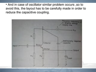
NIELIT, Gorakhpur
Major Factors in Designing Analog Circuit PCB
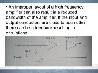
• 1 Component Placing
• 2 Signal Conductors
• 3 Supply and Ground Conductors
1. Component Placing
• Components which need access from the front plate
have to be exactly according to the instructions of the
equipment designer.
• Components for internal adjustment such as,
potentiometer , trimmer, switches etc have to be
arranged near the board edge and oriented in the proper
direction.
• Component with metal case should not be placed very
near to the access path that is needed for adjustment of
screw driver other wise short circuit may occur.
• Heat producing components are regularly distributed
over the entire board area, as far as it is feasible. This is
to avoid a locally overheated board.
• Hot components have to be separated from the board
surface by suitable surfacers.
• The locating of heat sensitive components must avoid a
close proximity to hot components as well as a place in a
flow of already warmed up air.
2. Signal Conductors
• Signal Conductors in analog circuit PCBs have to fulfill a
variety of different tasks, e.g. input, reference level,
feedback, output, etc.
• The length of any signal conductor should be made as
short as possible.This is because the magnitude of the
undesired inductive and capacitive coupling effects
increases more or less proportionally to the length of the
particular conductor.
• Apart from making of a good PCB, there are also other
techniques such as shielding or guarding with metallic
enclosures which have to be employed for a satisfactory
operation of equipment.
The signal conductor layout has to be done
particularly carefully for the following type of
circuits:
2.1 High Frequency Amplifiers/oscillators:
• At higher frequencies and with a long voltage supply line,
the circuit may oscillate because the voltage gain in an
emitter follower can be high i.e.,
Gain= Zcollector/Zemitter
• For precaution a capacitor is placed between the collector
and ground.
• And in case of oscillator similar problem occurs ,so to
avoid this, the layout has to be carefully made in order to
reduce the capacitive coupling.
• An improper layout of a high frequency
amplifier can also result in a reduced
bandwidth of the amplifier. If the input and
output conductors are close to each other ,
there can be a feedback resulting in
oscillations.
2.2 Multistage Amplifier with high power
output stage:
• If the ground and voltage conductors are long , a large
current I drawn by the high-power stage will flow through
the conductors with their own resistivity R.
• This additional resistance can modulate the Vcc and
GND of the input stage resulting in low frequency
oscillations which is called motorboating effect.
• To overcome this effect decoupling of the power supply
conductors with sufficiently large capacitor must be
done.
• Also separate Vcc and GND conductors can be provided
for two different stages.
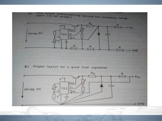
2.3 Feedback Amplifiers
• In designing high-wattage power supplies considerable
care in PCB layout design as well as in planning of the
remote sensing line to the front panel is necessary to
meet the regulation factor.
• A star grounding technique is used for the feedback
amplifier PCBs. The rectifier/capacitor circuit must be
connected to the star point for good cicuit performance.
2.4 High Gain DC Amplifiers(Thermal
Effects):
• When a device(transistor, DC amplifier) is soldered onto
the PCB, a thermocouple junction is formed between
copper( i.e. PCB conductor) and the kovar lead of the
transistor.
• If a temperature gradient exists, then different junctions
will create different voltages, thus effecting a noisy signal
to the amplifier.
2.5 Amplifier handling low level signals
a) Low level, high impedance:
Due to high impedance the capacitive coupling occurs . For
reducing the coupling , it is necessary to provide
sufficient distance between the high impedance
conductors and other interfering signal lines.
b) Low level, low Impedance:
If the impedance is low one has to be careful about induced
voltage due to magnetic fields or inductive coupling.
3. Supply and Ground Conductors
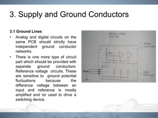
3.1 Ground Lines
• Analog and digital circuits on the
same PCB should strictly have
independent ground conductor
networks.
• There is one more type of circuit
part which should be provided with
separate ground conductors:
Reference voltage circuits. These
are sensitive to ground potential
fluctuations because the
difference voltage between an
input and reference is mostly
amplified and or used to drive a
switching device.
3.2 Supply Lines
• Supply lines have to be provided with sufficient width to
keep resistance and inductivity low.
• Supply lines are connceted to the circuit end with the
highest signal power level.
• Reference voltage circuits should tap with the supply
lines directly at the input to the PCB.
Discussion? Questions?

More Related Content

What's hot (20)

nota K pcb
nota K pcbnota K pcb
nota K pcb
 
Introduction to electronic circuit design..model
Introduction to electronic circuit design..modelIntroduction to electronic circuit design..model
Introduction to electronic circuit design..model
 
Diodes basics
Diodes   basicsDiodes   basics
Diodes basics
 
Diode
DiodeDiode
Diode
 
Introduction to Electronic Product Design
Introduction to Electronic Product DesignIntroduction to Electronic Product Design
Introduction to Electronic Product Design
 
MOSFET as a switch
MOSFET as a switchMOSFET as a switch
MOSFET as a switch
 
AVR_Course_Day1 basic electronics
AVR_Course_Day1 basic electronicsAVR_Course_Day1 basic electronics
AVR_Course_Day1 basic electronics
 
PCB Layout Fundamentals
PCB Layout FundamentalsPCB Layout Fundamentals
PCB Layout Fundamentals
 
Op-amp.pptx
Op-amp.pptxOp-amp.pptx
Op-amp.pptx
 
Basic MOSFET structure
Basic MOSFET structureBasic MOSFET structure
Basic MOSFET structure
 
Mosfet
MosfetMosfet
Mosfet
 
Function generator
Function generatorFunction generator
Function generator
 
Power electronics Introduction
Power electronics   IntroductionPower electronics   Introduction
Power electronics Introduction
 
pcb
pcbpcb
pcb
 
Chapter 5: Diode
Chapter 5: DiodeChapter 5: Diode
Chapter 5: Diode
 
Analog Layout and Process Concern
Analog Layout and Process ConcernAnalog Layout and Process Concern
Analog Layout and Process Concern
 
Rec101 unit iii operational amplifier
Rec101 unit iii operational amplifierRec101 unit iii operational amplifier
Rec101 unit iii operational amplifier
 
P1121110526
P1121110526P1121110526
P1121110526
 
Introduction to scr thyristers
Introduction to scr thyristersIntroduction to scr thyristers
Introduction to scr thyristers
 
Edc(electronics devices and circuits)
Edc(electronics devices and circuits)Edc(electronics devices and circuits)
Edc(electronics devices and circuits)
 

Viewers also liked

Printed Circuit Board Basics
Printed Circuit Board BasicsPrinted Circuit Board Basics
Printed Circuit Board BasicsSierra Assembly
 
Pcbdesign 140510145153-phpapp01
Pcbdesign 140510145153-phpapp01Pcbdesign 140510145153-phpapp01
Pcbdesign 140510145153-phpapp01ssantosh1234
 
Me88 art1 Product Design for Manufactrure and Assembly
Me88 art1 Product Design for Manufactrure and AssemblyMe88 art1 Product Design for Manufactrure and Assembly
Me88 art1 Product Design for Manufactrure and AssemblyDave Davidson
 
Design formanufacturingandassembly
Design formanufacturingandassemblyDesign formanufacturingandassembly
Design formanufacturingandassemblySathees Kumar
 
Value Engineering Introduction - K K B
Value Engineering Introduction - K K BValue Engineering Introduction - K K B
Value Engineering Introduction - K K BKumar Bhatt
 
Bare bone pcb,smt prototype stencil,pcb order ,production pcb supplier,rapid ...
Bare bone pcb,smt prototype stencil,pcb order ,production pcb supplier,rapid ...Bare bone pcb,smt prototype stencil,pcb order ,production pcb supplier,rapid ...
Bare bone pcb,smt prototype stencil,pcb order ,production pcb supplier,rapid ...raymingpcb
 
I450 laser marking machine presentation
I450 laser marking machine presentation I450 laser marking machine presentation
I450 laser marking machine presentation Guo Angela
 
SMT Equipment for PCB Assembly
SMT Equipment for PCB AssemblySMT Equipment for PCB Assembly
SMT Equipment for PCB AssemblyGuo Angela
 
pcb layers in layout
pcb layers in layoutpcb layers in layout
pcb layers in layoutAnum Mairaj
 
Smt Equipments (Pick And Place, Solder Paste Screen
Smt Equipments (Pick And Place, Solder Paste ScreenSmt Equipments (Pick And Place, Solder Paste Screen
Smt Equipments (Pick And Place, Solder Paste ScreenNaresh Sharma
 
Introduction to PCB Designing
Introduction to PCB DesigningIntroduction to PCB Designing
Introduction to PCB DesigningSharan kumar
 
SURFACE MOUNT TECHNOLOGY
SURFACE MOUNT TECHNOLOGYSURFACE MOUNT TECHNOLOGY
SURFACE MOUNT TECHNOLOGYSubhendra Singh
 
PCBA Assembly Process Flow / PCB Assembly Manufacturing
PCBA Assembly Process Flow / PCB Assembly ManufacturingPCBA Assembly Process Flow / PCB Assembly Manufacturing
PCBA Assembly Process Flow / PCB Assembly ManufacturingAgile Circuit Co., Ltd
 

Viewers also liked (20)

Printed Circuit Board Basics
Printed Circuit Board BasicsPrinted Circuit Board Basics
Printed Circuit Board Basics
 
Pcb designing
Pcb designingPcb designing
Pcb designing
 
Pcbdesign 140510145153-phpapp01
Pcbdesign 140510145153-phpapp01Pcbdesign 140510145153-phpapp01
Pcbdesign 140510145153-phpapp01
 
Me88 art1 Product Design for Manufactrure and Assembly
Me88 art1 Product Design for Manufactrure and AssemblyMe88 art1 Product Design for Manufactrure and Assembly
Me88 art1 Product Design for Manufactrure and Assembly
 
WelcomePCB
WelcomePCBWelcomePCB
WelcomePCB
 
Design formanufacturingandassembly
Design formanufacturingandassemblyDesign formanufacturingandassembly
Design formanufacturingandassembly
 
Value Engineering Introduction - K K B
Value Engineering Introduction - K K BValue Engineering Introduction - K K B
Value Engineering Introduction - K K B
 
Bare bone pcb,smt prototype stencil,pcb order ,production pcb supplier,rapid ...
Bare bone pcb,smt prototype stencil,pcb order ,production pcb supplier,rapid ...Bare bone pcb,smt prototype stencil,pcb order ,production pcb supplier,rapid ...
Bare bone pcb,smt prototype stencil,pcb order ,production pcb supplier,rapid ...
 
I450 laser marking machine presentation
I450 laser marking machine presentation I450 laser marking machine presentation
I450 laser marking machine presentation
 
SMT Equipment for PCB Assembly
SMT Equipment for PCB AssemblySMT Equipment for PCB Assembly
SMT Equipment for PCB Assembly
 
Smt tht pcb design and manufacture
Smt tht pcb design and manufactureSmt tht pcb design and manufacture
Smt tht pcb design and manufacture
 
Pcb layout
Pcb layoutPcb layout
Pcb layout
 
Wave soldering 101
Wave soldering 101Wave soldering 101
Wave soldering 101
 
Surface Mount Technology
 Surface Mount Technology Surface Mount Technology
Surface Mount Technology
 
pcb layers in layout
pcb layers in layoutpcb layers in layout
pcb layers in layout
 
Smt Equipments (Pick And Place, Solder Paste Screen
Smt Equipments (Pick And Place, Solder Paste ScreenSmt Equipments (Pick And Place, Solder Paste Screen
Smt Equipments (Pick And Place, Solder Paste Screen
 
Introduction to PCB Designing
Introduction to PCB DesigningIntroduction to PCB Designing
Introduction to PCB Designing
 
SURFACE MOUNT TECHNOLOGY
SURFACE MOUNT TECHNOLOGYSURFACE MOUNT TECHNOLOGY
SURFACE MOUNT TECHNOLOGY
 
PCBA Assembly Process Flow / PCB Assembly Manufacturing
PCBA Assembly Process Flow / PCB Assembly ManufacturingPCBA Assembly Process Flow / PCB Assembly Manufacturing
PCBA Assembly Process Flow / PCB Assembly Manufacturing
 
SMT
SMTSMT
SMT
 

Similar to Analog Design Considerations in PCB.

Electronic Components
Electronic ComponentsElectronic Components
Electronic ComponentsArnab Bhaumik
 
ESL 130- ELECTRICAL & ELECTRONICS WORKSHOP.pdf
ESL 130- ELECTRICAL & ELECTRONICS WORKSHOP.pdfESL 130- ELECTRICAL & ELECTRONICS WORKSHOP.pdf
ESL 130- ELECTRICAL & ELECTRONICS WORKSHOP.pdfagnelmiriam
 
33/11 KV TRANSMISSION LINE
33/11 KV TRANSMISSION LINE 33/11 KV TRANSMISSION LINE
33/11 KV TRANSMISSION LINE Lalit Kumar
 
Applications and functions of ferrites
Applications and functions of ferritesApplications and functions of ferrites
Applications and functions of ferritesShivam Padmani
 
Section 5b&c capacitors pn junction
Section 5b&c capacitors  pn junctionSection 5b&c capacitors  pn junction
Section 5b&c capacitors pn junctionCDI Aljeer
 
Meas of current.pptx
Meas of current.pptxMeas of current.pptx
Meas of current.pptxAnkitKachhap4
 
Analog Electronics - Basics - Part-1
Analog Electronics - Basics - Part-1Analog Electronics - Basics - Part-1
Analog Electronics - Basics - Part-1MEENAKSHISUNDARAVELS
 
Switchyard final
Switchyard finalSwitchyard final
Switchyard finalHAIDER ALI
 
Presentation 12v dc to 230v ac 100 wat invertor
Presentation 12v dc to 230v ac 100 wat invertorPresentation 12v dc to 230v ac 100 wat invertor
Presentation 12v dc to 230v ac 100 wat invertormirzaahmadali
 
PCB Layout guidelines.pdf
PCB Layout guidelines.pdfPCB Layout guidelines.pdf
PCB Layout guidelines.pdfssuserf36d4d1
 
Omg! The Best 278 Pcb Layout Design Specifications Ever!
Omg! The Best 278 Pcb Layout Design Specifications Ever!Omg! The Best 278 Pcb Layout Design Specifications Ever!
Omg! The Best 278 Pcb Layout Design Specifications Ever!PaddyWang4
 
Wireless driven led semiconductor lightning system
Wireless driven led  semiconductor lightning systemWireless driven led  semiconductor lightning system
Wireless driven led semiconductor lightning systemAnand Parakkat Parambil
 
2. Transmitter and Reciver microwave optical communication
2. Transmitter and Reciver microwave optical communication2. Transmitter and Reciver microwave optical communication
2. Transmitter and Reciver microwave optical communicationbfrfelix714
 
Ceramic Capacitor final
Ceramic Capacitor finalCeramic Capacitor final
Ceramic Capacitor finalNeelam Chopade
 
Mosquito repellent circuit
Mosquito  repellent circuitMosquito  repellent circuit
Mosquito repellent circuitSagnik Dasgupta
 

Similar to Analog Design Considerations in PCB. (20)

Electronic Components
Electronic ComponentsElectronic Components
Electronic Components
 
UNIT_5 PPT-MBM.pptx
UNIT_5 PPT-MBM.pptxUNIT_5 PPT-MBM.pptx
UNIT_5 PPT-MBM.pptx
 
ESL 130- ELECTRICAL & ELECTRONICS WORKSHOP.pdf
ESL 130- ELECTRICAL & ELECTRONICS WORKSHOP.pdfESL 130- ELECTRICAL & ELECTRONICS WORKSHOP.pdf
ESL 130- ELECTRICAL & ELECTRONICS WORKSHOP.pdf
 
33/11 KV TRANSMISSION LINE
33/11 KV TRANSMISSION LINE 33/11 KV TRANSMISSION LINE
33/11 KV TRANSMISSION LINE
 
Applications and functions of ferrites
Applications and functions of ferritesApplications and functions of ferrites
Applications and functions of ferrites
 
Section 5b&c capacitors pn junction
Section 5b&c capacitors  pn junctionSection 5b&c capacitors  pn junction
Section 5b&c capacitors pn junction
 
Meas of current.pptx
Meas of current.pptxMeas of current.pptx
Meas of current.pptx
 
Analog Electronics - Basics - Part-1
Analog Electronics - Basics - Part-1Analog Electronics - Basics - Part-1
Analog Electronics - Basics - Part-1
 
Switchyard final
Switchyard finalSwitchyard final
Switchyard final
 
Presentation 12v dc to 230v ac 100 wat invertor
Presentation 12v dc to 230v ac 100 wat invertorPresentation 12v dc to 230v ac 100 wat invertor
Presentation 12v dc to 230v ac 100 wat invertor
 
PCB Layout guidelines.pdf
PCB Layout guidelines.pdfPCB Layout guidelines.pdf
PCB Layout guidelines.pdf
 
Omg! The Best 278 Pcb Layout Design Specifications Ever!
Omg! The Best 278 Pcb Layout Design Specifications Ever!Omg! The Best 278 Pcb Layout Design Specifications Ever!
Omg! The Best 278 Pcb Layout Design Specifications Ever!
 
Ecm pre amplifier
Ecm pre amplifierEcm pre amplifier
Ecm pre amplifier
 
PCB
PCBPCB
PCB
 
Wireless driven led semiconductor lightning system
Wireless driven led  semiconductor lightning systemWireless driven led  semiconductor lightning system
Wireless driven led semiconductor lightning system
 
2. Transmitter and Reciver microwave optical communication
2. Transmitter and Reciver microwave optical communication2. Transmitter and Reciver microwave optical communication
2. Transmitter and Reciver microwave optical communication
 
Special diodes.ppt
Special diodes.pptSpecial diodes.ppt
Special diodes.ppt
 
Ceramic Capacitor final
Ceramic Capacitor finalCeramic Capacitor final
Ceramic Capacitor final
 
Mosquito repellent circuit
Mosquito  repellent circuitMosquito  repellent circuit
Mosquito repellent circuit
 
Power Electronics
Power ElectronicsPower Electronics
Power Electronics
 

Recently uploaded

Hostel management system project report..pdf
Hostel management system project report..pdfHostel management system project report..pdf
Hostel management system project report..pdfKamal Acharya
 
Call Girls In Bangalore ☎ 7737669865 🥵 Book Your One night Stand
Call Girls In Bangalore ☎ 7737669865 🥵 Book Your One night StandCall Girls In Bangalore ☎ 7737669865 🥵 Book Your One night Stand
Call Girls In Bangalore ☎ 7737669865 🥵 Book Your One night Standamitlee9823
 
VIP Call Girls Palanpur 7001035870 Whatsapp Number, 24/07 Booking
VIP Call Girls Palanpur 7001035870 Whatsapp Number, 24/07 BookingVIP Call Girls Palanpur 7001035870 Whatsapp Number, 24/07 Booking
VIP Call Girls Palanpur 7001035870 Whatsapp Number, 24/07 Bookingdharasingh5698
 
XXXXXXXXXXXXXXXXXXXXXXXXXXXXXXXXXXXXXXXXXXXXXXXXXXXX
XXXXXXXXXXXXXXXXXXXXXXXXXXXXXXXXXXXXXXXXXXXXXXXXXXXXXXXXXXXXXXXXXXXXXXXXXXXXXXXXXXXXXXXXXXXXXXXXXXXXXXXX
XXXXXXXXXXXXXXXXXXXXXXXXXXXXXXXXXXXXXXXXXXXXXXXXXXXXssuser89054b
 
Thermal Engineering Unit - I & II . ppt
Thermal Engineering  Unit - I & II . pptThermal Engineering  Unit - I & II . ppt
Thermal Engineering Unit - I & II . pptDineshKumar4165
 
data_management_and _data_science_cheat_sheet.pdf
data_management_and _data_science_cheat_sheet.pdfdata_management_and _data_science_cheat_sheet.pdf
data_management_and _data_science_cheat_sheet.pdfJiananWang21
 
Bhosari ( Call Girls ) Pune 6297143586 Hot Model With Sexy Bhabi Ready For ...
Bhosari ( Call Girls ) Pune  6297143586  Hot Model With Sexy Bhabi Ready For ...Bhosari ( Call Girls ) Pune  6297143586  Hot Model With Sexy Bhabi Ready For ...
Bhosari ( Call Girls ) Pune 6297143586 Hot Model With Sexy Bhabi Ready For ...tanu pandey
 
Introduction to Serverless with AWS Lambda
Introduction to Serverless with AWS LambdaIntroduction to Serverless with AWS Lambda
Introduction to Serverless with AWS LambdaOmar Fathy
 
Work-Permit-Receiver-in-Saudi-Aramco.pptx
Work-Permit-Receiver-in-Saudi-Aramco.pptxWork-Permit-Receiver-in-Saudi-Aramco.pptx
Work-Permit-Receiver-in-Saudi-Aramco.pptxJuliansyahHarahap1
 
Design For Accessibility: Getting it right from the start
Design For Accessibility: Getting it right from the startDesign For Accessibility: Getting it right from the start
Design For Accessibility: Getting it right from the startQuintin Balsdon
 
Call Girls Wakad Call Me 7737669865 Budget Friendly No Advance Booking
Call Girls Wakad Call Me 7737669865 Budget Friendly No Advance BookingCall Girls Wakad Call Me 7737669865 Budget Friendly No Advance Booking
Call Girls Wakad Call Me 7737669865 Budget Friendly No Advance Bookingroncy bisnoi
 
Double Revolving field theory-how the rotor develops torque
Double Revolving field theory-how the rotor develops torqueDouble Revolving field theory-how the rotor develops torque
Double Revolving field theory-how the rotor develops torqueBhangaleSonal
 
Navigating Complexity: The Role of Trusted Partners and VIAS3D in Dassault Sy...
Navigating Complexity: The Role of Trusted Partners and VIAS3D in Dassault Sy...Navigating Complexity: The Role of Trusted Partners and VIAS3D in Dassault Sy...
Navigating Complexity: The Role of Trusted Partners and VIAS3D in Dassault Sy...Arindam Chakraborty, Ph.D., P.E. (CA, TX)
 
Hazard Identification (HAZID) vs. Hazard and Operability (HAZOP): A Comparati...
Hazard Identification (HAZID) vs. Hazard and Operability (HAZOP): A Comparati...Hazard Identification (HAZID) vs. Hazard and Operability (HAZOP): A Comparati...
Hazard Identification (HAZID) vs. Hazard and Operability (HAZOP): A Comparati...soginsider
 
Thermal Engineering -unit - III & IV.ppt
Thermal Engineering -unit - III & IV.pptThermal Engineering -unit - III & IV.ppt
Thermal Engineering -unit - III & IV.pptDineshKumar4165
 
FULL ENJOY Call Girls In Mahipalpur Delhi Contact Us 8377877756
FULL ENJOY Call Girls In Mahipalpur Delhi Contact Us 8377877756FULL ENJOY Call Girls In Mahipalpur Delhi Contact Us 8377877756
FULL ENJOY Call Girls In Mahipalpur Delhi Contact Us 8377877756dollysharma2066
 

Recently uploaded (20)

Hostel management system project report..pdf
Hostel management system project report..pdfHostel management system project report..pdf
Hostel management system project report..pdf
 
Call Girls In Bangalore ☎ 7737669865 🥵 Book Your One night Stand
Call Girls In Bangalore ☎ 7737669865 🥵 Book Your One night StandCall Girls In Bangalore ☎ 7737669865 🥵 Book Your One night Stand
Call Girls In Bangalore ☎ 7737669865 🥵 Book Your One night Stand
 
VIP Call Girls Palanpur 7001035870 Whatsapp Number, 24/07 Booking
VIP Call Girls Palanpur 7001035870 Whatsapp Number, 24/07 BookingVIP Call Girls Palanpur 7001035870 Whatsapp Number, 24/07 Booking
VIP Call Girls Palanpur 7001035870 Whatsapp Number, 24/07 Booking
 
XXXXXXXXXXXXXXXXXXXXXXXXXXXXXXXXXXXXXXXXXXXXXXXXXXXX
XXXXXXXXXXXXXXXXXXXXXXXXXXXXXXXXXXXXXXXXXXXXXXXXXXXXXXXXXXXXXXXXXXXXXXXXXXXXXXXXXXXXXXXXXXXXXXXXXXXXXXXX
XXXXXXXXXXXXXXXXXXXXXXXXXXXXXXXXXXXXXXXXXXXXXXXXXXXX
 
Thermal Engineering Unit - I & II . ppt
Thermal Engineering  Unit - I & II . pptThermal Engineering  Unit - I & II . ppt
Thermal Engineering Unit - I & II . ppt
 
Cara Menggugurkan Sperma Yang Masuk Rahim Biyar Tidak Hamil
Cara Menggugurkan Sperma Yang Masuk Rahim Biyar Tidak HamilCara Menggugurkan Sperma Yang Masuk Rahim Biyar Tidak Hamil
Cara Menggugurkan Sperma Yang Masuk Rahim Biyar Tidak Hamil
 
data_management_and _data_science_cheat_sheet.pdf
data_management_and _data_science_cheat_sheet.pdfdata_management_and _data_science_cheat_sheet.pdf
data_management_and _data_science_cheat_sheet.pdf
 
Bhosari ( Call Girls ) Pune 6297143586 Hot Model With Sexy Bhabi Ready For ...
Bhosari ( Call Girls ) Pune  6297143586  Hot Model With Sexy Bhabi Ready For ...Bhosari ( Call Girls ) Pune  6297143586  Hot Model With Sexy Bhabi Ready For ...
Bhosari ( Call Girls ) Pune 6297143586 Hot Model With Sexy Bhabi Ready For ...
 
Introduction to Serverless with AWS Lambda
Introduction to Serverless with AWS LambdaIntroduction to Serverless with AWS Lambda
Introduction to Serverless with AWS Lambda
 
Integrated Test Rig For HTFE-25 - Neometrix
Integrated Test Rig For HTFE-25 - NeometrixIntegrated Test Rig For HTFE-25 - Neometrix
Integrated Test Rig For HTFE-25 - Neometrix
 
Work-Permit-Receiver-in-Saudi-Aramco.pptx
Work-Permit-Receiver-in-Saudi-Aramco.pptxWork-Permit-Receiver-in-Saudi-Aramco.pptx
Work-Permit-Receiver-in-Saudi-Aramco.pptx
 
Design For Accessibility: Getting it right from the start
Design For Accessibility: Getting it right from the startDesign For Accessibility: Getting it right from the start
Design For Accessibility: Getting it right from the start
 
Call Girls Wakad Call Me 7737669865 Budget Friendly No Advance Booking
Call Girls Wakad Call Me 7737669865 Budget Friendly No Advance BookingCall Girls Wakad Call Me 7737669865 Budget Friendly No Advance Booking
Call Girls Wakad Call Me 7737669865 Budget Friendly No Advance Booking
 
Double Revolving field theory-how the rotor develops torque
Double Revolving field theory-how the rotor develops torqueDouble Revolving field theory-how the rotor develops torque
Double Revolving field theory-how the rotor develops torque
 
Water Industry Process Automation & Control Monthly - April 2024
Water Industry Process Automation & Control Monthly - April 2024Water Industry Process Automation & Control Monthly - April 2024
Water Industry Process Automation & Control Monthly - April 2024
 
Navigating Complexity: The Role of Trusted Partners and VIAS3D in Dassault Sy...
Navigating Complexity: The Role of Trusted Partners and VIAS3D in Dassault Sy...Navigating Complexity: The Role of Trusted Partners and VIAS3D in Dassault Sy...
Navigating Complexity: The Role of Trusted Partners and VIAS3D in Dassault Sy...
 
Call Girls in Ramesh Nagar Delhi 💯 Call Us 🔝9953056974 🔝 Escort Service
Call Girls in Ramesh Nagar Delhi 💯 Call Us 🔝9953056974 🔝 Escort ServiceCall Girls in Ramesh Nagar Delhi 💯 Call Us 🔝9953056974 🔝 Escort Service
Call Girls in Ramesh Nagar Delhi 💯 Call Us 🔝9953056974 🔝 Escort Service
 
Hazard Identification (HAZID) vs. Hazard and Operability (HAZOP): A Comparati...
Hazard Identification (HAZID) vs. Hazard and Operability (HAZOP): A Comparati...Hazard Identification (HAZID) vs. Hazard and Operability (HAZOP): A Comparati...
Hazard Identification (HAZID) vs. Hazard and Operability (HAZOP): A Comparati...
 
Thermal Engineering -unit - III & IV.ppt
Thermal Engineering -unit - III & IV.pptThermal Engineering -unit - III & IV.ppt
Thermal Engineering -unit - III & IV.ppt
 
FULL ENJOY Call Girls In Mahipalpur Delhi Contact Us 8377877756
FULL ENJOY Call Girls In Mahipalpur Delhi Contact Us 8377877756FULL ENJOY Call Girls In Mahipalpur Delhi Contact Us 8377877756
FULL ENJOY Call Girls In Mahipalpur Delhi Contact Us 8377877756
 

Analog Design Considerations in PCB.

  • 1. Design Rules For Analog Circuit PCB Presented By:- Shovana Khan Yusufzai M.Tech in E.D&T NIELIT, Gorakhpur
  • 2. Major Factors in Designing Analog Circuit PCB • 1 Component Placing • 2 Signal Conductors • 3 Supply and Ground Conductors
  • 3. 1. Component Placing • Components which need access from the front plate have to be exactly according to the instructions of the equipment designer. • Components for internal adjustment such as, potentiometer , trimmer, switches etc have to be arranged near the board edge and oriented in the proper direction. • Component with metal case should not be placed very near to the access path that is needed for adjustment of screw driver other wise short circuit may occur.
  • 4. • Heat producing components are regularly distributed over the entire board area, as far as it is feasible. This is to avoid a locally overheated board. • Hot components have to be separated from the board surface by suitable surfacers. • The locating of heat sensitive components must avoid a close proximity to hot components as well as a place in a flow of already warmed up air.
  • 5. 2. Signal Conductors • Signal Conductors in analog circuit PCBs have to fulfill a variety of different tasks, e.g. input, reference level, feedback, output, etc. • The length of any signal conductor should be made as short as possible.This is because the magnitude of the undesired inductive and capacitive coupling effects increases more or less proportionally to the length of the particular conductor. • Apart from making of a good PCB, there are also other techniques such as shielding or guarding with metallic enclosures which have to be employed for a satisfactory operation of equipment.
  • 6. The signal conductor layout has to be done particularly carefully for the following type of circuits: 2.1 High Frequency Amplifiers/oscillators: • At higher frequencies and with a long voltage supply line, the circuit may oscillate because the voltage gain in an emitter follower can be high i.e., Gain= Zcollector/Zemitter • For precaution a capacitor is placed between the collector and ground.
  • 7. • And in case of oscillator similar problem occurs ,so to avoid this, the layout has to be carefully made in order to reduce the capacitive coupling.
  • 8. • An improper layout of a high frequency amplifier can also result in a reduced bandwidth of the amplifier. If the input and output conductors are close to each other , there can be a feedback resulting in oscillations.
  • 9. 2.2 Multistage Amplifier with high power output stage:
  • 10. • If the ground and voltage conductors are long , a large current I drawn by the high-power stage will flow through the conductors with their own resistivity R. • This additional resistance can modulate the Vcc and GND of the input stage resulting in low frequency oscillations which is called motorboating effect. • To overcome this effect decoupling of the power supply conductors with sufficiently large capacitor must be done. • Also separate Vcc and GND conductors can be provided for two different stages.
  • 11. 2.3 Feedback Amplifiers • In designing high-wattage power supplies considerable care in PCB layout design as well as in planning of the remote sensing line to the front panel is necessary to meet the regulation factor. • A star grounding technique is used for the feedback amplifier PCBs. The rectifier/capacitor circuit must be connected to the star point for good cicuit performance.
  • 12.
  • 13. 2.4 High Gain DC Amplifiers(Thermal Effects): • When a device(transistor, DC amplifier) is soldered onto the PCB, a thermocouple junction is formed between copper( i.e. PCB conductor) and the kovar lead of the transistor. • If a temperature gradient exists, then different junctions will create different voltages, thus effecting a noisy signal to the amplifier.
  • 14. 2.5 Amplifier handling low level signals a) Low level, high impedance: Due to high impedance the capacitive coupling occurs . For reducing the coupling , it is necessary to provide sufficient distance between the high impedance conductors and other interfering signal lines. b) Low level, low Impedance: If the impedance is low one has to be careful about induced voltage due to magnetic fields or inductive coupling.
  • 15. 3. Supply and Ground Conductors 3.1 Ground Lines • Analog and digital circuits on the same PCB should strictly have independent ground conductor networks. • There is one more type of circuit part which should be provided with separate ground conductors: Reference voltage circuits. These are sensitive to ground potential fluctuations because the difference voltage between an input and reference is mostly amplified and or used to drive a switching device.
  • 16. 3.2 Supply Lines • Supply lines have to be provided with sufficient width to keep resistance and inductivity low. • Supply lines are connceted to the circuit end with the highest signal power level. • Reference voltage circuits should tap with the supply lines directly at the input to the PCB.