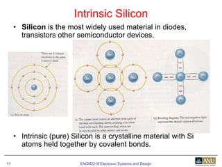
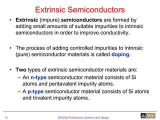
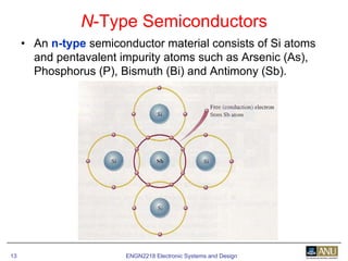
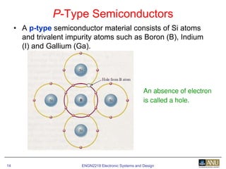
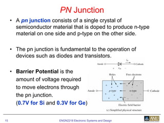
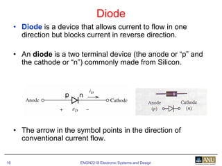
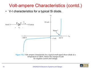
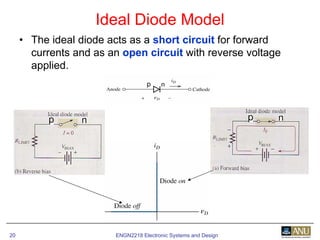
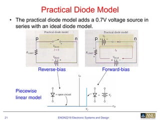
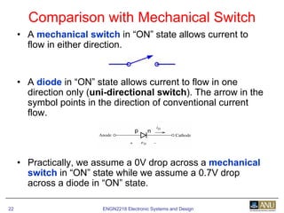
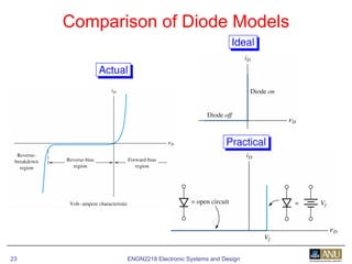
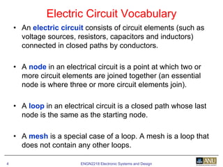
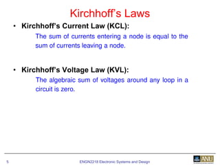
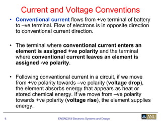
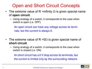
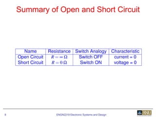
This document provides an overview of diodes and semiconductor physics. It defines key concepts like intrinsic and extrinsic semiconductors, n-type and p-type materials, and pn junctions. It describes how a diode allows current to flow in one direction due to the structure of the pn junction. The diode is modeled as an ideal diode in parallel with a 0.7V voltage source to account for its forward voltage drop. Diodes act as uni-directional switches compared to mechanical switches which conduct current bidirectionally.

![ENGN2218 Electronic Systems and Design10
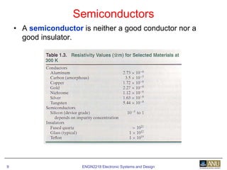
• Electronic devices such as diodes and transistors are
made of a semiconductor material.
• A basic knowledge of semiconductor physics helps us to
understand diode and bipolar junction transistor
behaviour.
• Common semiconductor materials are
– Silicon (Si) [single-element semiconductor]
– Germanium (Ge) [single-element semiconductor]
– Carbon (C) [single-element semiconductor]
– Gallium Arsenide (GaAs) [compound semiconductor]
Basic Semiconductor Concepts](https://image.slidesharecdn.com/week01dioderevisionrevision-150705232129-lva1-app6891/85/Week01-diode-revision-revision-10-320.jpg)