More Related Content Similar to Lect2 up090 (100324) Similar to Lect2 up090 (100324) (20) 1. Lecture 090 – Large Signal MOSFET Model (3/24/10) Page 090-1
LECTURE 090 – LARGE SIGNAL MOSFET MODEL
LECTURE ORGANIZATION
Outline
• Introduction to modeling
• Operation of the MOS transistor
• Simple large signal model (SAH model)
• Subthreshold model
• Short channel, strong inversion model
• Summary
CMOS Analog Circuit Design, 2nd Edition Reference
Pages 73-78 and 97-99
CMOS Analog Circuit Design © P.E. Allen - 2010
Lecture 090 – Large Signal MOSFET Model (3/24/10) Page 090-2
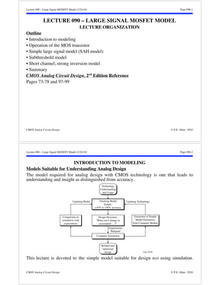
INTRODUCTION TO MODELING
Models Suitable for Understanding Analog Design
The model required for analog design with CMOS technology is one that leads to
understanding and insight as distinguished from accuracy.
Technology
Understanding
and Usage
Thinking Model
Updating Model Updating Technology
Simple,
±10% to ±50% accuracy
Design Decisions-
"What can I change to
accomplish ....?"
Expectations
"Ballpark"
Computer Simulation
Extraction of Simple
Model Parameters
from Computer Models
Comparison of
simulation with
expectations
Refined and
optimized
design
Fig.3.0-02
This lecture is devoted to the simple model suitable for design not using simulation.
CMOS Analog Circuit Design © P.E. Allen - 2010
2. Lecture 090 – Large Signal MOSFET Model (3/24/10) Page 090-3
Categorization of Electrical Models
Time Dependence
Time Independent Time Dependent
Linearity
Linear Small-signal, midband
Rin, Av, Rout
(.TF)
Small-signal frequency
response-poles and zeros
(.AC)
Nonlinear DC operating point
iD = f(vD,vG,vS,vB)
(.OP)
Large-signal transient
response - Slew rate
(.TRAN)
Based on the simulation capabilities of SPICE.
CMOS Analog Circuit Design © P.E. Allen - 2010
Lecture 090 – Large Signal MOSFET Model (3/24/10) Page 090-4
OPERATION OF THE MOS TRANSISTOR
Formation of the Channel for an Enhancement MOS Transistor
Subthreshold (VG<VT)
VB = 0 VS = 0 VG < VT VD = 0
Polysilicon
n+
n+
Depletion Region
Polysilicon
p+
p- substrate
Threshold (VG=VT)
VB = 0 VS = 0 VG =VT VD = 0
p+
n+ n+
p- substrate
n+ n+
Fig.3.1-02
Inverted Region
Strong Threshold (VGVT)
VB = 0 VS = 0 VG VT VD = 0
Polysilicon
p+
p- substrate
Inverted Region
CMOS Analog Circuit Design © P.E. Allen - 2010
3. Lecture 090 – Large Signal MOSFET Model (3/24/10) Page 090-5
Transconductance Characteristics of an Enhancement NMOSFET when VDS = 0.1V
VB = 0 VS = 0 vG =VT VD = 0.1V
Polysilicon
n+ n+
Depletion Region
Polysilicon
p+
p- substrate
iD
VB = 0 VS = 0 VG = 2VT VD = 0.1V
p+
VGS=2VT:
n+ n+
p- substrate
vGS
vGS
vGS
Fig.3.1-03
iD
Inverted Region
VB = 0 VS = 0 VG = 3VT VD = 0.1V
Polysilicon
p+
VGS=3VT:
n+ n+
p- substrate
VGS≤VT:
Inverted Region
iD
0 VT 2VT 3VT
0
iD
0 VT 2VT 3VT
0
iD
0 VT 2VT 3VT
0
CMOS Analog Circuit Design © P.E. Allen - 2010
Lecture 090 – Large Signal MOSFET Model (3/24/10) Page 090-6
Output Characteristics of the Enhancement NMOS Transistor for VGS = 2VT
VGS = 2VT
vDS
VGS = 2VT
vDS
VGS = 2VT
vDS
Fig.3.1-04
vG =2VT VD = 0V
VB = 0 VS = 0
n+ n+
p- substrate
VDS=0.5VT:
Polysilicon
p+
Inverted Region
iD
Polysilicon
VB = 0 VS = 0 VG = 2VT VD = 0.5VT
p+
n+ n+
p- substrate Channel current
iD
VB = 0 VS = 0 VD =VT
VDS=0:
iD
0 0.5VT VT
0
VDS=VT:
VG = 2VT
iD
0 0.5VT VT
0
iD
0 0.5VT VT
0
Polysilicon
p+
n+
p- substrate
A depletion region
iD
n+
forms between the drain and channel
CMOS Analog Circuit Design © P.E. Allen - 2010
4. Lecture 090 – Large Signal MOSFET Model (3/24/10) Page 090-7
Output Characteristics of the Enhanced NMOS when vDS = 2VT
vDS
vDS
vDS
VGS =VT
VGS =2VT
VGS =3VT
Fig.3.1-05
vG =VT
VD = 2VT
Polysilicon
VB = 0 VS = 0
p+
n+ n+
p- substrate
iD
Polysilicon
VB = 0 VS = 0 VG = 2VT VD = 2VT
p+
n+ n+
p- substrate
VB = 0 VS = 0
VGS=VT:
iD
0 VT 2VT
0
VGS=2VT:
VGS=3VT:
VG = 3VT
Polysilicon
iD
VD = 2VT
p+
n+n+
p- substrate
iD
iD
0
0
iD
0
0
3VT
VT 2VT 3VT
VT 2VT 3VT
Further increase in
VG will cause the FET to become active
CMOS Analog Circuit Design © P.E. Allen - 2010
Lecture 090 – Large Signal MOSFET Model (3/24/10) Page 090-8
Output Characteristics of an Enhancement NMOS Transistor
SPICE Input File:
2000
1500
1000
500
iD(μA)
Output Characteristics for NMOS
M1 6 1 0 0 MOS1 w=5u l=1.0u
VGS1 1 0 1.0
M2 6 2 0 0 MOS1 w=5u l=1.0u
VGS2 2 0 1.5
M3 6 3 0 0 MOS1 w=5u l=1.0u
VGS3 3 0 2.0
M4 6 4 0 0 MOS1 w=5u l=1.0u
VGS4 4 0 2.5
VGS = 3.0
VGS = 2.5
VGS = 2.0
VGS = 1.5
VGS = 1.0
0 1 2 3 4 5
vDS (Volts)
Fig. 3.1-6
M5 6 5 0 0 MOS1 w=5u l=1.0u
VGS5 5 0 3.0
VDS 6 0 5
.model mos1 nmos (vto=0.7 kp=110u
+gamma=0.4 +lambda=.04 phi=.7)
.dc vds 0 5 .2
.print dc ID(M1), ID(M2), ID(M3), ID(M4),
ID(M5)
.end
0
CMOS Analog Circuit Design © P.E. Allen - 2010
5. Lecture 090 – Large Signal MOSFET Model (3/24/10) Page 090-9
Transconductance Characteristics of an Enhancement NMOS Transistor
SPICE Input File:
6000
5000
4000
3000
2000
1000
0
VDS = 5V
VDS = 4V
VDS = 2V
VDS = 1V
VDS = 3V
0 1 2 3 4 5
iD(μA)
Transconductance Characteristics for NMOS
M1 1 6 0 0 MOS1 w=5u l=1.0u
VDS1 1 0 1.0
M2 2 6 0 0 MOS1 w=5u l=1.0u
VDS2 2 0 2.0
M3 3 6 0 0 MOS1 w=5u l=1.0u
VDS3 3 0 3.0
M4 4 6 0 0 MOS1 w=5u l=1.0u
VDS4 4 0 4.0
vGS (Volts)
Fig. 3.1-7
M5 5 6 0 0 MOS1 w=5u l=1.0u
VDS5 5 0 5.0
VGS 6 0 5
.model mos1 nmos (vto=0.7 kp=110u
+gamma=0.4 lambda=.04 phi=.7)
.dc vgs 0 5 .2
.print dc ID(M1), ID(M2), ID(M3), ID(M4),
ID(M5)
.probe
.end
CMOS Analog Circuit Design © P.E. Allen - 2010
Lecture 090 – Large Signal MOSFET Model (3/24/10) Page 090-10
SIMPLE LARGE SIGNAL MODEL (SAH MODEL)
Large Signal Model Derivation
1.) Let the charge per unit area in the channel
inversion layer be
QI(y) = -Cox[vGS-v(y)-VT] (coul./cm2)
+
-
vGS +
iD vD
n+ n+
2.) Define sheet conductivity of the inversion
layer per square as
S = μoQI(y)
cm2
v·s
7. amps
volt =
Source Drain
0 y y+dy L p-
1
/sq.
3.) Ohm's Law for current in a sheet is
JS =
iD
W = -SEy = -S
dv
dy dv =
-iD
SW dy =
y
v(y)
dy
-
Fig.110-03
-iDdy
μoQI(y)W iD dy = -WμoQI(y)dv
4.) Integrating along the channel for 0 to L gives
vDS
WμoQI(y)dv =
L
iDdy = -
0
0
vDS
WμoCox[vGS-v(y)-VT]dv
0
5.) Evaluating the limits gives
iD =
WμoCox
L
v2(y)
2
(vGS-VT)v(y)-
vDS
0
WμoCox
iD=
L
vDS2
2
(vGS-VT)vDS-
CMOS Analog Circuit Design © P.E. Allen - 2010
8. Lecture 090 – Large Signal MOSFET Model (3/24/10) Page 090-11
Saturation Voltage - VDS(sat)
Interpretation of the large
signal model:
vDS = vGS-VT
Active Region Saturation Region
iD
The saturation voltage for
MOSFETs is the value of drain-source voltage at
the peak of the inverted parabolas.
diD
dvDS =
μoCoxW
L [(vGS-VT) - vDS] = 0
vDS(sat)=vGS-VT
Useful definitions:
μoCoxW
L =
K’W
L =
Increasing
values of
vDS
vGS
Fig. 110-04
vDS
vGS
Cutoff Saturation Active
0
0 Fig. 3.2-4
VT
vDS = vGS - VT
CMOS Analog Circuit Design © P.E. Allen - 2010
Lecture 090 – Large Signal MOSFET Model (3/24/10) Page 090-12
The Simple Large Signal MOSFET Model
Regions of Operation of the MOS Transistor:
1.) Cutoff Region:
vGS - VT 0
iD = 0
(Ignores subthreshold currents)
2.) Active Region
0 vDS vGS - VT
iD =
μoCoxW
2L
2(vGS-VT)-vDS vDS
3.) Saturation Region
0 vGS - VT vDS
μoCoxW
iD =
2L
vGS-VT
2
Output Characteristics of the MOSFET:
iD/ID0
1.0
0.75
0.5
0.25
vDS = vGS-VT
Active
Region Saturation Region
Channel modulation effects
Cutoff Region
0
0 0.5 1.0 1.5 2.0 2.5
vGS-VT
VGS0-VT
vGS-VT
VGS0-VT
vGS-VT
VGS0-VT
vGS-VT
VGS0-VT
= 1.0
= 0.86
= 0.70
= 0.5
= 0
vGS-VT
VGS0-VT
vDS
VGS0-VT
Fig. 110-05
CMOS Analog Circuit Design © P.E. Allen - 2010
9. Lecture 090 – Large Signal MOSFET Model (3/24/10) Page 090-13
Illustration of the Need to Account for the Influence of vDS on the Simple Sah Model
Compare the Simple Sah model to SPICE level 2:
K' = 44.8μA/V
k=0.5, v (sat)
= 1.0V
SPICE Level 2
K' = 29.6μA/V
k = 0, v (sat)
= 1.0V
K' = 44.8μA/V
k = 0, v (sat)
= 1.0V
2
DS
DS
2
DS
2
0 0.2 0.4 0.6 0.8 1
25μA
20μA
15μA
10μA
5μA
0μA
vDS (volts)
iD
VGS = 2.0V, W/L = 100μm/100μm, and no mobility effects.
CMOS Analog Circuit Design © P.E. Allen - 2010
Lecture 090 – Large Signal MOSFET Model (3/24/10) Page 090-14
Modification of the Previous Model to Include the Effects of vDS on VT
From the previous derivation:
vDS
WμoQI(y)dv =
L
iDdy = -
0
0
vDS
WμoCox[vGS-v(y)-VT]dv
0
Assume that the threshold voltage varies across the channel in the following way:
VT(y) = VT + kv(y)
where VT is the value of VT the at the source end of the channel and k is a constant.
Integrating the above gives,
iD =
WμoCox
L
v2(y)
2
(vGS-VT)v(y)-(1+k)
vDS
0
or
iD =
WμoCox
L
v2DS
2
(vGS-VT)vDS-(1+k)
To find vDS(sat), set the diD/dvDS equal to zero and solve for vDS = vDS(sat),
vDS(sat) =
vGS-VT
1+k
Therefore, in the saturation region, the drain current is
iD =
WμoCox
2(1+k)L (vGS - VT)2
For k = 0.5 and K’ = 44.8μA/V2, excellent correlation is achieved with SPICE 2
CMOS Analog Circuit Design © P.E. Allen - 2010
10. Lecture 090 – Large Signal MOSFET Model (3/24/10) Page 090-15
Influence of vDS on the Output Characteristics
Channel modulation effect:
As the value of vDS increases, the
effective L decreases causing the
current to increase.
Illustration:
Note that Leff = L - Xd
Therefore the model in saturation
becomes,
iD =
K’W
2Leff (vGS-VT)2
Depletion
Region
B S
n+n+
p- substrate
diD
dvDS = -
VG VT VD VDS(sat)
Polysilicon
p+
K’W
2Leff2 (vGS - VT)2
Leff
dLeff
dvDS =
Xd
iD
Leff
Fig110-06
dXd
dvDS iD
Therefore, a good approximation to the influence of vDS on iD is
iD iD( = 0) +
diD
dvDS vDS = iD( = 0)(1 + vDS) =
K’W
2L (vGS-VT)2(1+vDS)
CMOS Analog Circuit Design © P.E. Allen - 2010
Lecture 090 – Large Signal MOSFET Model (3/24/10) Page 090-16
Channel Length Modulation Parameter,
Assume the MOS is transistor is saturated-
iD =
μCoxW
2L (vGS - VT)2(1 + vDS)
Define iD(0) = iD when vDS = 0V.
iD(0) =
μCoxW
2L (vGS- VT)2
Now,
iD = iD(0)[1 + vDS] = iD(0) + iD(0) vDS
Matching with y = mx + b gives the value of
iD3(0 VGS3
VGS2
VGS1
vDS
iD
-1
)
iD2(0)
iD1(0)
CMOS Analog Circuit Design © P.E. Allen - 2010
11. Lecture 090 – Large Signal MOSFET Model (3/24/10) Page 090-17
Influence of Channel Length on
Note that the value of varies with channel length, L. The data below is from a 0.25μm
CMOS technology.
0.6
0.5
0.4
0.3
0.2
0.1
0
PMOS
NMOS
0 0.5 1 1.5 2 2.5
Channel Length Modulation (V-1)
Channel Length (microns)
Fig.130-6
Most analog designers stay away from minimum channel length to get better gains and
matching at the sacrifice of speed.
CMOS Analog Circuit Design © P.E. Allen - 2010
Lecture 090 – Large Signal MOSFET Model (3/24/10) Page 090-18
Influence of the Bulk Voltage on the Large Signal MOSFET Model
The components of the threshold voltage
are:
VT = Gate-bulk work function (MS)
+ voltage to change the surface
potential (-2F)
+ voltage to offset the channel-bulk
depletion charge (-Qb/Cox)
+ voltage to compensate the
undesired interface charge
(-Qss/Cox)
We know that
Qb = |2F|+|vBS|
Therefore, as the bulk becomes more
reverse biased with respect to the
source, the threshold voltage must
increase to offset the increased channel-bulk
depletion charge.
VD 0
VBS0 = 0V VGS
n+ n+
VD 0
iD
iD
VBS1 0V VGS
Polysilicon
n+ n+
VD 0
iD = 0
VSB2 VSB1: VGS
n+ n+
060613-02
VSB0 = 0:
VSB1 0:
p- substrate
p- substrate
VSB2 VSB1:
Polysilicon
Polysilicon
p+
p+
p+
p- substrate
CMOS Analog Circuit Design © P.E. Allen - 2010
12. Lecture 090 – Large Signal MOSFET Model (3/24/10) Page 090-19
Influence of the Bulk Voltage on the Large Signal MOSFET Model - Continued
Bulk-Source (vBS) influence on the transconductance characteristics-
Decreasing values
of bulk-source voltage
vGS
060612-02
VBS = 0
iD
vDS vGS-VT
VT0 VT1 VT2 VT3
ID
VGS
In general, the simple model incorporates the bulk effect into VT by the previously
developed relationship:
VT(vBS) = VT0 + 2|f|+|vBS| - 2|f|
CMOS Analog Circuit Design © P.E. Allen - 2010
Lecture 090 – Large Signal MOSFET Model (3/24/10) Page 090-20
Summary of the Simple Large Signal MOSFET Model
N-channel reference convention:
Non-saturation-iD
=
WμoCox
L
vDS2
2 (1 + vDS)
(vGS-VT)vDS-
Saturation-iD
=
WμoCox
L
vDS(sat)2
(vGS-VT)vDS(sat)-
2 (1+vDS)=
G
iD
+
vGS
WμoCox
D
B
+
+
vBS
-
S
vDS
-
Fig. 110-10
2L (vGS-VT)2(1+vDS)
where:
μo = zero field mobility (cm2/volt·sec)
Cox = gate oxide capacitance per unit area (F/cm2)
= channel-length modulation parameter (volts-1)
VT = VT0 + 13. 2|f|+|vBS|- 2|f|
VT0 = zero bias threshold voltage
= bulk threshold parameter (volts-0.5)
2|f| = strong inversion surface potential (volts)
For p-channel MOSFETs, use n-channel equations with p-channel parameters and invert
the current.
CMOS Analog Circuit Design © P.E. Allen - 2010
14. Lecture 090 – Large Signal MOSFET Model (3/24/10) Page 090-21
Silicon Constants
Constant
Symbol
Constant Description Value Units
VG
k
ni
o
si
ox
Silicon bandgap (27°C)
Boltzmann’s constant
Intrinsic carrier concentration (27°C)
Permittivity of free space
Permittivity of silicon
Permittivity of SiO2
1.205
1.381x10⁻²³
1.45x10¹⁰
8.854x10⁻¹⁴
11.7 o
3.9 o
V
J/K
cm-3
F/cm
F/cm
F/cm
CMOS Analog Circuit Design © P.E. Allen - 2010
Lecture 090 – Large Signal MOSFET Model (3/24/10) Page 090-22
MOSFET Parameters
Model Parameters for a Typical CMOS Bulk Process (0.25μm CMOS n-well):
Parameter Parameter Description
Typical Parameter Value
Symbol
N-Channel P-Channel
Units
VT0 Threshold Voltage
(VBS = 0)
0.5± 0.15 -0.5 ± 0.15 V
K' Transconductance Para-meter
(in saturation)
120.0 ± 10% 25.0 ± 10% μA/V2
Bulk threshold
parameter
0.4 0.6 (V)1/2
Channel length
modulation parameter
0.32 (L=Lmin)
0.06 (L 2Lmin)
0.56 (L=Lmin)
0.08 (L 2Lmin)
(V)-1
2|F| Surface potential at
strong inversion
0.7 0.8 V
CMOS Analog Circuit Design © P.E. Allen - 2010
15. Lecture 090 – Large Signal MOSFET Model (3/24/10) Page 090-23
SUBTHRESHOLD MODEL
Large-Signal Model for Weak Inversion
The electrons in the substrate at the source side can be expressed as,
s
Vt
np(0) = npoexp
16. The electrons in the substrate at the drain side can be expressed as,
s-vDS
Vt
np(L) = npoexp
20. vDS
Vt
-
where X is the thickness of the region in which iD flows.
In weak inversion, the changes in the surface potential, s are controlled by changes in
the gate-source voltage, vGS, through a voltage divider consisting of Cox and Cjs, the
depletion region capacitance.
ds
dvGS =
Cox
Cox+Cjs =
1n
s =
vGS
n + k1 =
vGS-VT
n + k2
where
Cox
Cjs φs
060405-04
Poly
Oxide
Channel
Dep.
Substrate
vGS
k2 = k1 +
VT
n
CMOS Analog Circuit Design © P.E. Allen - 2010
Lecture 090 – Large Signal MOSFET Model (3/24/10) Page 090-24
Large-Signal Model for Weak Inversion – Continued
Substituting the above relationships back into the expression for iD gives,
iD =
WL
qXDnnpo exp
k2
Vt exp
26. vDS
Vt
-
Define It as
It = qXDnnpo exp
k2
Vt
32. vDS
Vt
-
where n 1.5 – 3
If vDS 0, then
iD = It
WL exp
vGS-VT
nVt
35. vDS
VA
1+
The boundary between nonsaturated
and saturated is found as,
Vov = VDS(sat) = VON = VGS -VT = 2nVt
VGS=VT
VGSVT
iD
1μA
0 0 vDS 1V
Fig. 140-03
CMOS Analog Circuit Design © P.E. Allen - 2010
36. Lecture 090 – Large Signal MOSFET Model (3/24/10) Page 090-25
SHORT CHANNEL, STRONG INVERSION MODEL
What is Velocity Saturation?
The most important short-channel
effect in MOSFETs is the velocity
saturation of carriers in the channel.
A plot of electron drift velocity
versus electric field is shown below.
An expression for the electron drift
velocity as a function of the electric
field is,
vd
μnE
1+E/Ec
where
105
5x10⁴
2x10⁴
104
5x10³
105 106 107
Electric Field (V/m)
Electron Drift Velocity (m/s)
vd = electron drift velocity (m/s)
μn = low-field mobility ( 0.07m2/V·s)
Ec = critical electrical field at which velocity saturation occurs
Fig130-1
CMOS Analog Circuit Design © P.E. Allen - 2010
Lecture 090 – Large Signal MOSFET Model (3/24/10) Page 090-26
Short-Channel Model Derivation
As before,
JD = JS =
iD
W = QI(y)vd(y) iD = WQI(y)vd(y) =
WQI(y)μnE
1+E/Ec iD
E
Ec = WQI(y)μnE
1+
Replacing E by dv/dy gives,
iD
dv
dy = WQI(y)μn
1
Ec
1+
dv
dy
Integrating along the channel gives,
L
iD
0
vDS
WQI(y)μndv
dv
dy dy =
1
Ec
1+
0
The result of this integration is,
μnCox
iD =
2
vDS
L
1
Ec
1+
WL
[2(vGS-VT)vDS-vDS2] =
μnCox
2
1+vDS
WL
[2(vGS-VT)vDS-vDS2]
where = 1/(EcL) with dimensions of V-1.
CMOS Analog Circuit Design © P.E. Allen - 2010
37. Lecture 090 – Large Signal MOSFET Model (3/24/10) Page 090-27
Saturation Voltage
Differentiating iD with respect to vDS and setting equal to zero gives,
V’DS(sat) =
1
1+2(VGS-VT-1 (VGS-VT)
(VGS-VT)
1-
2 +···
if
(VGS-VT)
2 1
Therefore,
V’DS(sat) VDS(sat)
(VGS-VT)
1-
2 +···
Note that the transistor will enter the saturation region for vDS vGS - VT in the
presence of velocity saturation.
CMOS Analog Circuit Design © P.E. Allen - 2010
Lecture 090 – Large Signal MOSFET Model (3/24/10) Page 090-28
Large Signal Model for the Saturation Region
Assuming that
(VGS-VT)
2 1
gives
V’DS(sat) (VGS-VT)
Therefore the large signal model in the saturation region becomes,
iD =
K’
2[1+(vGS-VT)]
WL
[ vGS - VT]2, vDS (VGS-VT)
(VGS-VT)
1-
2 +···
CMOS Analog Circuit Design © P.E. Allen - 2010
38. Lecture 090 – Large Signal MOSFET Model (3/24/10) Page 090-29
The Influence of Velocity Saturation on the Transconductance Characteristics
The following plot was made for K’ = 110μA/V2 and W/L = 1:
1000
800
600
400
200
0
θ = 0
θ = 0.2
θ = 0.4
θ = 0.6
θ = 0.8
θ = 1.0
0.5 1 1.5 2 2.5 3
iD/W (μA/μm)
vGS (V)
Fig130-2
Note as the velocity saturation effect becomes stronger, that the drain current-gate
voltage relationship becomes linear.
CMOS Analog Circuit Design © P.E. Allen - 2010
Lecture 090 – Large Signal MOSFET Model (3/24/10) Page 090-30
Circuit Model for Velocity Saturation
A simple circuit model to include the influence of velocity saturation is
is shown:
We know that
iD =
K’W
2L (vGS’ -VT)2 and vGS = vGS’ + iD RSX
or
vGS’ = vGS - iDRXS
Substituting vGS’ into the current relationship gives,
iD =
K’W
2L (vGS - iDRSX -VT)2
Solving for iD results in,
iD =
K’
2
WL
1+K’
RSX(vGS-VT)
WL
(vGS - VT)2
Comparing with the previous result, we see that
= K’
WL
RSX RSX =
L
K’W =
1
EcK’W
Therefore for K’ = 110μA/V2, W = 1μm and Ec = 1.5x10⁶V/m, we get RSX = 6.06k.
CMOS Analog Circuit Design © P.E. Allen - 2010
39. Lecture 090 – Large Signal MOSFET Model (3/24/10) Page 090-31
SUMMARY
• The modeling of this lecture is devoted to understanding how the circuit works
• The two primary current-voltage characteristics of the MOSFET are the
transconductance characteristic and the output characteristic
• The simple Sah large signal model is good enough for most applications and technology
• The Sah model can be improved in the region of the knee and for the weak dependence
of drain current on drain-source voltage in the saturation region
• Most designers do not work at minimum channel length because of the channel length
modulation effect and because worse matching occurs for small areas
• The threshold voltage is increased as the bulk-source is reverse biased
• The subthreshold model accounts for very small currents that flow in the channel when
the gate-source voltage is smaller than the threshold voltage
• The subthreshold current is exponentially related to the gate-source voltage
• Velocity saturation occurs at minimum channel length and can be modeled by including
a source degeneration resistor with the simple large signal model
CMOS Analog Circuit Design © P.E. Allen - 2010