More Related Content Similar to Lect2 up320 (100328) Similar to Lect2 up320 (100328) (20) 1. Lecture 320 – Improved Open-Loop Comparators and Latches (3/28/10) Page 320-1
LECTURE 320 – IMPROVED OPEN-LOOP COMPARATORS
AND LATCHES
LECTURE ORGANIZATION
Outline
• Autozeroing
• Hysteresis
• Simple Latches
• Summary
CMOS Analog Circuit Design, 2nd Edition Reference
Pages 464-483
CMOS Analog Circuit Design © P.E. Allen - 2010
Lecture 320 – Improved Open-Loop Comparators and Latches (3/28/10) Page 320-2
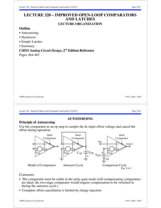
AUTOZEROING
Principle of Autozeroing
Use the comparator as an op amp to sample the dc input offset voltage and cancel the
offset during operation.
Comparator
+ -
-
Ideal
Comparator
+ -
Ideal
VOS VOS
vIN vOUT
CAZ VOS
+
VOS
+
-
Comparator
+ -
VOS
Ideal
CAZ
Model of Comparator. Autozero Cycle Comparison Cycle
Fig. 8.4-1
Comments:
• The comparator must be stable in the unity-gain mode (self-compensating comparators
are ideal, the two-stage comparator would require compensation to be switched in
during the autozero cycle.)
• Complete offset cancellation is limited by charge injection
CMOS Analog Circuit Design © P.E. Allen - 2010
2. Lecture 320 – Improved Open-Loop Comparators and Latches (3/28/10) Page 320-3
Differential Implementation of Autozeroed Comparators
+
-
VOS
Ideal
φ1
Comparator
φ2 + -
+ -
VOS
CAZ
vIN-vOUT
φ1
φ1
VOS
vOUT = VOS
Comparator during φ1 phase
+ - + -
VOS
VOS
vOUT
φ2
vIN-Lecture
vIN+
Differential Autozeroed Comparator Comparator during φ2 phase
Fig. 8.4-2
vIN+
CMOS Analog Circuit Design © P.E. Allen - 2010
320 – Improved Open-Loop Comparators and Latches (3/28/10) Page 320-4
Single-Ended Autozeroed Comparators
Noninverting:
vOUT vIN
+ -
φ2
φ2
φ1 CAZ
φ1
φ1
Fig. 8.4-3
Inverting:
vIN vOUT
+ -
φ2
CAZ
φ1
φ1
Fig. 8.4-4
Comment on autozeroing:
Need to be careful about noise that gets sampled onto the autozeroing capacitor and
is present on the comparison phase of the process.
CMOS Analog Circuit Design © P.E. Allen - 2010
3. Lecture 320 – Improved Open-Loop Comparators and Latches (3/28/10) Page 320-5
HYSTERESIS
Influence of Input Noise on the Comparator
Comparator without hysteresis:
vin
vout
Comparator
threshold
VOH
VOL
t
t
Fig. 8.4-6A
Comparator with hysteresis:
vin
vout
VTRP+
VTRP-Fig.
VOH
VOL
t
t
8.4-6B
CMOS Analog Circuit Design © P.E. Allen - 2010
Lecture 320 – Improved Open-Loop Comparators and Latches (3/28/10) Page 320-6
Use of Hysteresis for Comparators in a Noisy Environment
Transfer curve of a comparator with hysteresis:
vOUT
VTRP+
vIN
VTRP-VOH
VOL
(VOH-VOL) VTRP+
vIN
Fig. 8.4-5
vOUT
VOH
VOL
0
0
R1
R2
VTRP-Counterclockwise
Bistable Clockwise Bistable
Hysteresis is achieved by the use of positive feedback
• Externally
• Internally
CMOS Analog Circuit Design © P.E. Allen - 2010
4. Lecture 320 – Improved Open-Loop Comparators and Latches (3/28/10) Page 320-7
Noninverting Comparator using External Positive Feedback
Circuit:
Upper Trip Point:
Assume that vOUT =
R2
+-
vIN R1
Fig. 8.4-7
VOL, the upper trip point occurs when,
0 =
R1
R1+R2
VOL +
R2
R1+R2
VTRP
vOUT
R1VOH
R2
-
+ VTRP
R1
R2
+ = -
vOUT
(VOH-VOL) -
0
R1
R2
VOH
VOL
0
VOL
Lower Trip Point:
Assume that vOUT = VOH, the lower trip point occurs when,
0 =
R1
R1+R2
VOH +
R2
R1+R2
VTRP
- VTRP
- = -
R1
R2
VOH
Width of the bistable characteristic:
Vin = VTRP+-VTRP- =
R1
R2
VOH-VOL
R1VOL
R2
vIN
CMOS Analog Circuit Design © P.E. Allen - 2010
Lecture 320 – Improved Open-Loop Comparators and Latches (3/28/10) Page 320-8
Inverting Comparator using External Positive Feedback
Circuit:
+ -
vOUT
vIN
R1
R2
vOUT
vIN
VOH
(VOH-VOL)
0
0
R1
R1+R2
R1VOL R1VOH
R1+R2 R1+R2
VOL
Fig. 8.4-8
Upper Trip Point:
vIN = VTRP
+ =
R1
R1+R2
VOH
Lower Trip Point:
vIN = VTRP
- =
R1
R1+R2
VOL
Width of the bistable characteristic:
Vin = VTRP+-VTRP- =
R1
R1+R2
VOH-VOL
CMOS Analog Circuit Design © P.E. Allen - 2010
5. Lecture 320 – Improved Open-Loop Comparators and Latches (3/28/10) Page 320-9
Horizontal Shifting of the CCW Bistable Characteristic
Circuit:
Upper Trip Point:
VREF =
R1
R1+R2
vIN R1
VREF
Fig. 8.4-9
VOL +
R2
R1+R2
R2
+-
VTRP
vOUT
VOH
VOL
vOUT
0
0
+ VTRP
R1
R2
(VOH-VOL)
R1+R2
R2
VREF
R1VOH
R2
+ =
R1|VOL|
R2
R1+R2
R2
VREF -
vIN
R1
R2
VOL
Lower Trip Point:
VREF =
R1
R1+R2
VOH +
R2
R1+R2
VTRP
- VTRP
- =
R1+R2
R2
VREF -
R1
R2
VOH
Shifting Factor:
±
R2
R1+R2
VREF
CMOS Analog Circuit Design © P.E. Allen - 2010
Lecture 320 – Improved Open-Loop Comparators and Latches (3/28/10) Page 320-10
Horizontal Shifting of the CW Bistable Characteristic
Circuit:
+ -
vOUT
vIN
R1 R2
vIN
R1 (VOH-VOL)
Fig. 8.4-10
VREF
vOUT
VOH
0
VOL
R1+R2
R2 VREF
R1+R2
R1|VOL|
0
R1VOH
R1+R2
R1+R2
Upper Trip Point:
vIN = VTRP
+ =
R1
R1+R2
VOH +
R2
R1+R2
VREF
Lower Trip Point:
vIN = VTRP
- =
R1
R1+R2
VOL +
R2
R1+R2
VREF
Shifting Factor:
±
R2
R1+R2
VREF
CMOS Analog Circuit Design © P.E. Allen - 2010
6. Lecture 320 – Improved Open-Loop Comparators and Latches (3/28/10) Page 320-11
Example 320-1 Design of an Inverting Comparator with Hysteresis
Use the inverting bistable to design a high-gain, open-loop comparator having an
upper trip point of 1V and a lower trip point of 0V if VOH = 2V and VOL = -2V.
Solution
Putting the values of this example into the above relationships gives
1 =
R1
R1+R2
2 +
R2
R1+R2
VREF
and
0 =
R1
R1+R2
(-2) +
R2
R1+R2
VREF
Solving these two equations gives 3R1 = R2 and VREF = (2/3)V.
CMOS Analog Circuit Design © P.E. Allen - 2010
Lecture 320 – Improved Open-Loop Comparators and Latches (3/28/10) Page 320-12
Hysteresis using Internal Positive Feedback
Simple comparator with internal positive feedback:
VDD
M3 M6 M7 M4
vo1 vo2
vi1 M1 M2 vi2
M8 M5
VSS
IBias
Fig. 8.4-11
CMOS Analog Circuit Design © P.E. Allen - 2010
7. Lecture 320 – Improved Open-Loop Comparators and Latches (3/28/10) Page 320-13
Internal Positive Feedback - Upper Trip Point
Assume that the gate of M1 is on ground and the
input to M2 is much smaller than zero. The
resulting circuit is:
M1 on, M2 off M3 on, M6 on (active), M4 and
M7 off.
vo2 is high.
M6 wants to source the current i6 =
W6/L6
W3/L3
i1
As vin begins to increase towards the trip point, the
current flow through M2 increases. When i2 = i6,
the upper trip point will occur.
i5 = i1+i2 = i3+i6 = i3+ 9. W6/L6
W3/L3
i3 = i3
W6/L6
W3/L3
1+
VDD
M3 M6 M7 M4
vo1 vo2
M1 M2
i1 = i3
i1 = i3 =
i2 = i6
i5
M5
VSS
vin
Fig. 8.4-12A
I5
1+[(W6/L6)/(W3/L3)]
Also, i2 = i5 - i1 = i5 - i3
Knowing i1 and i2 allows the calculation of vGS1 and vGS2 which gives
VTRP+ = vGS2 - vGS1 =
2i2
2
+ VT2 -
2i1
1
- VT1
CMOS Analog Circuit Design © P.E. Allen - 2010
Lecture 320 – Improved Open-Loop Comparators and Latches (3/28/10) Page 320-14
Internal Positive Feedback - Lower Trip Point
Assume that the gate of M1 is on ground and the input
to M2 is much greater than zero. The resulting circuit
is:
M2 on, M1 off M4 and M7 on, M3 and M6 off.
vo1 is high.
M7 wants to source the current i7 =
W7/L7
W4/L4
i2
As vin begins to decrease towards the trip point, the
current flow through M1 increases. When i1 = i7, the
lower trip point will occur.
i5 = i1+i2 = i7+i4 = 11. W7/L7
W4/L4
i4 +i4 = i4
W7/L7
W4/L4
1+
VDD
M3 M6 M7 M4
vo1 vo2
vi1
M1 M2
i2 = i4 =
i1 = i7
M5
I5
i2 = i4
vi1
V Fig. 8.4-12B SS
i5
vi
1+[(W7/L7)/(W4/L4)]
Also, i1 = i5 - i2 = i5 - i4
Knowing i1 and i2 allows the calculation of vGS1 and vGS2 which gives
VTRP- = vGS2 - vGS1 =
2i2
2 + VT2 -
2i1
1 - VT1
CMOS Analog Circuit Design © P.E. Allen - 2010
12. Lecture 320 – Improved Open-Loop Comparators and Latches (3/28/10) Page 320-15
Example 320-2 - Calculation of Trip Voltages for a Comparator with Hysteresis
Consider the circuit shown. If KN’ = 110μA/V2,
KP’ = 50μA/V2, and VTN = |VTP| = 0.7V,
calculate the positive and negative threshold
points if the device lengths are all 1 μm and the
widths are given as: W1 = W2 = W6 = W7 = 10 μm
and W3 = W4 = 2 μm. The gate of M1 is tied to
ground and the input is the gate of M2. The
current, i5 = 20 μA
Solution
To calculate the positive trip point, assume
that the input has been negative and is heading
positive.
i6 =
(W/L)6
(W/L)3 i3 = (5/1)(i3) i3 =
i5
IBias
VDD
M3 M6 M7 M4
vo1 vo2
vi1 M1 M2 vi2
M8 M5
1+[(W/L)6/(W/L)3] = i1 =
VSS
Fig. 8.4-11
20μA
1+5 = 3.33 μA
i2 = i5 i1 = 20 3.33 = 16.67 μA vGS1 =
2i1
1
1/2
+VT1 =
2·3.33
(5)110
1/2
+0.7 = 0.81V
vGS2 =
2i2
2
1/2
+ VT2 =
2·16.67
(5)110
1/2
+ 0.7 = 0.946V
VTRP+ vGS2vGS1 = 0.9460.810 = 0.136V
CMOS Analog Circuit Design © P.E. Allen - 2010
Lecture 320 – Improved Open-Loop Comparators and Latches (3/28/10) Page 320-16
Example 320-2 - Continued
Determining the negative trip point, similar analysis yields
i4 = 3.33 μA
i1 = 16.67 μA
vGS2 = 0.81V
vGS1 = 0.946V
VTRP- vGS2 vGS1 = 0.81 0.946 = 0.136V
PSPICE simulation results of this circuit are shown below.
2.6
2.4
2.2
2
1.8
1.6
1.4
1.2
1
-0.5 -0.4 -0.3 -0.2 -0.1 0.0 0.1 0.2 0.3 0.4 0.5
vo2
(volts)
vin (volts) Fig. 8.4-13
CMOS Analog Circuit Design © P.E. Allen - 2010
13. Lecture 320 – Improved Open-Loop Comparators and Latches (3/28/10) Page 320-17
Complete Comparator with Internal Hysteresis
VDD
M3 M6 M7 M4
M9 M8
vi1 vi2
M1 M2
M10 M11
M8 M5
VSS
IBias
vout
Fig. 8.4-14
CMOS Analog Circuit Design © P.E. Allen - 2010
Lecture 320 – Improved Open-Loop Comparators and Latches (3/28/10) Page 320-18
Schmitt Trigger
The Schmitt trigger is a circuit that has better defined switching points.
Consider the following circuit:
How does this circuit work?
Assume the input voltage, vin, is low and the output
voltage, vout , is high.
M3, M4 and M5 are on and M1, M2 and M6 are off.
When vin is increased from zero, M2 starts to turn on causing
M3 to start turning off. Positive feedback causes M2 to turn
on further and eventually both M1 and M2 are on and the
output is at zero.
The upper switching point, VTRP+ is found as follows:
When vin is low, the voltage at the source of M2 (M3) is
vS2 = VDD-VTN3
VTRP+ = vin when M2 turns on given as VTRP+ = VTN2 + vS2
vin
VDD
M3
M5
M4
M2
M1
M6
vout
Fig. 8.4-15
VTRP+ occurs when the input voltage causes the currents in M3 and M1 to be equal.
CMOS Analog Circuit Design © P.E. Allen - 2010
14. Lecture 320 – Improved Open-Loop Comparators and Latches (3/28/10) Page 320-19
Schmitt Trigger – Continued
Thus, iD1 = 1( VTRP+ - VTN1)2 = 3( VDD - vS2- VTN3) 2 = iD3
which can be written as, assuming that VTN2 = VTN3,
1( VTRP+ - VTN1) 2 = 3( VDD – VTRP+)2 VTRP+ =
VTN1+ 3/1VDD
1+ 3/1
The switching point, VTRP- is found in a similar manner and is:
5( VDD - VTRP- - VTP5)2 = 6( VTRP-)2 VTRP- =
5/6(VDD-VTP5)
1+ 5/6
The bistable characteristic is,
vin
vout
VDD
VDD
0 0 VTRP- VTRP+
Fig. 8.4-16
CMOS Analog Circuit Design © P.E. Allen - 2010
Lecture 320 – Improved Open-Loop Comparators and Latches (3/28/10) Page 320-20
SIMPLE LATCHES
Regenerative Comparators
Regenerative comparators use positive feedback to accomplish the comparison of two
signals. Latches can have a faster switching speed than the previous comparators.
NMOS and PMOS latch:
VDD
I1 I2
vo1 vo2
M1 M2
VDD
M1 M2
vo1 vo2
I1 I2
Fig. 8.5-3
NMOS latch PMOS latch
CMOS Analog Circuit Design © P.E. Allen - 2010
15. Lecture 320 – Improved Open-Loop Comparators and Latches (3/28/10) Page 320-21
Operating Modes of the Latch
The latch has two modes of operation – enable or latch and Enable (enable_bar) or Latch
(latch_bar).
1.) During the Enable_bar, the latch is turned off (currents are removed) and the
unknown inputs are applied to it. The parasitic capacitance at the latch nodes hold the
unknown voltage.
2.) During Enable, the latch is turned on, and the positive feedback acts on the applied
inputs and causes one side of the latch to go high and the other side to go low.
Enable_bar:
Enable Enable
Vo2ʼ
060808-09
VDD
I1 I2
Enable Enable
M1 M2
Vo1ʼ
VDD
M1 M2
I1 I2
Vo2ʼ Vo1ʼ
NMOS latch PMOS latch
The inputs are initially applied to the outputs of the latch.
Vo1’ = initial input applied to vo1
CMOS Analog Circuit Design © P.E. Allen - 2010
Lecture 320 – Improved Open-Loop Comparators and Latches (3/28/10) Page 320-22
Step Response of a Latch (Enable)
Circuit:
Ri and Ci are the
resistance and capacitance
seen to ground from the
i-th transistor.
Nodal equations:
gm1Vo2+G1Vo1+sC1
VDD VDD
I1 I2
vo2
M1 M2
vo1
+
+
Vo2 Vo1
gm1Vo2 R1
C1
Vo1'
s
-
-
gm2Vo1 R2
Vo1’
s = gm1Vo2+G1Vo1+sC1V o1-C1Vo1’ = 0
Vo1-
gm2Vo1+G2Vo2+sC2
Vo2’
s = gm2Vo1+G2Vo2+sC2V o2-C2Vo2’ = 0
Vo2-
Solving for Vo1 and Vo2 gives,
Vo1 =
R1C1
sR1C1+1 Vo1’ -
gm1R1
sR1C1+1 Vo2 =
1
s1+1 Vo1’ -
gm1R1
s1+1 Vo2
Vo2 =
R2C2
sR2C2+1 Vo2’ -
gm2R2
sR2C2+1 Vo1 =
2
s2+1 Vo2’ -
gm2R2
s2+1 Vo1
Defining the output, Vo, and input, Vi, as
Vo = Vo2-Vo1 and Vi = Vo2’-Vo1’
C2
Vo2'
s
+
Vo2
-
Fig. 8.5-4
CMOS Analog Circuit Design © P.E. Allen - 2010
16. Lecture 320 – Improved Open-Loop Comparators and Latches (3/28/10) Page 320-23
Step Response of the Latch - Continued
Solving for Vo gives,
Vo = Vo2-Vo1 =
s+1 Vi +
gmR
s+1 Vo
or
Vo =
Vi
s+(1-gmR) =
Vi
1-gmR
s
1-gmR+1
=
’Vi
s’+1
where
’ =
1-gmR
Taking the inverse Laplace transform gives
vo(t) = Vi e-t/’ = Vi e-t(1-gmR) / egmRt/Vi, if gmR 1.
Define the latch time constant as
L = |’|
gmR =
C
gm
=
0.67WLCox
2K’(W/L)I = 0.67Cox
WL3
2K’I
if C Cgs.
Vout(t) = et/L Vi
CMOS Analog Circuit Design © P.E. Allen - 2010
Lecture 320 – Improved Open-Loop Comparators and Latches (3/28/10) Page 320-24
Step Response of a Latch - Continued
Normalize the output voltage by (VOH-VOL) to get
Vout(t)
VOH-VOL
= et/L
Vi
VOH-VOL
which is plotted as,
The propagation delay time is
tp = L ln
VOH-VOL
2Vi
Note that the larger the Vi, the
faster the response.
1
0.8
0.6
0.5
0.4 0.3
0.2
0.1
0.05
ΔVi
VOH-VOL
0.03
ΔVout
VOH-VOL 0.01
0.4
0.2
0
0.005
0 1 2 t 3 4 5
τL
Fig. 8.5-5
CMOS Analog Circuit Design © P.E. Allen - 2010
17. Lecture 320 – Improved Open-Loop Comparators and Latches (3/28/10) Page 320-25
Example 320-3 - Time Domain Characteristics of a Latch.
Find the propagation time delay for the NMOS if the W/L of the latch transistors is
5μm/0.5μm and the latch dc current is 10μA when Vi = 0.1(VOH-VOL) and Vi =
0.01(VOH-VOL).
Solution
The transconductance of the latch transistors is
gm = 2·120·10·10 = 155μS
The output conductance is 0.6μS which gives gmR of 93V/V. Since gmR is greater than
1, we can use the above results. Therefore the latch time constant is found as
L = 0.67Cox
WL3
2K’I = 0.67(60.6x10⁻⁴)
(5·0.5)x10-24
2·120x10-6·10x10-6 = 0.131ns
Since the propagation time delay is the time when the output is 0.5(VOH-VOL), then
using the above results or Fig. 8.5-5 we find for Vi = 0.01(VOH-VOL) that tp = 3.91L =
0.512ns and for Vi = 0.1(VOH-VOL) that tp = 1.61L = 0.211ns.
CMOS Analog Circuit Design © P.E. Allen - 2010
Lecture 320 – Improved Open-Loop Comparators and Latches (3/28/10) Page 320-26
Comparator using a Latch with a Built-In Reference†
How does it operate?
1.) Devices in shaded region operate in the
triode region.
2.) When the latch/reset goes high, the upper
cross-coupled inverter-latch regenerates. The
drain currents of M5 and M6 are steered to
obtain a final state determined by the mismatch
between the R1 and R2 resistances.
1
R1 = KN
W1
L (vin+-VT)+
W2
L (VREF--VT)
and
1
R2 = KN
W1
L (vin--VT)+
W2
L (VREF+-VT)
φ1 φ1
Latch
/Reset
Latch
/Rese
φ1 φ1
vout-
M9
M3
R1 R2
M1
M7
M5
M8
M2 M2
M1
M10
M4
M6
vin+ vin-vout+
VREF- VREF+
3.) The input voltage which causes R1 = R2 is vin(threshold) = (W2/W1)VREF
W2/W1 = 1/4 generates a threshold of ±0.25VREF.
VDD
Fig. 8.5-6
Performance 20Ms/s 200μW
† T.B. Cho and P.R. Gray, “A 10b, 20Msamples/s, 35mW pipeline A/D Converter,” IEEE J. Solid-State Circuits, vol. 30, no. 3, pp. 166-172, March
1995.
CMOS Analog Circuit Design © P.E. Allen - 2010
18. Lecture 320 – Improved Open-Loop Comparators and Latches (3/28/10) Page 320-27
Simple, Low Power Latched Comparator†
VDD
φ1 φ1
φ1 φ1
vout-
M9
M3
M7
M5
M10
M4
M8
M6
vin+ vin-vout+
M1
M2
Fig. 8.5-7
Dissipated 50μW when clocked at 2MHz.
Self-referenced
† A. Coban, “1.5V, 1mW, 98-dB Delta-Sigma ADC”, Ph.D. dissertation, School of ECE, Georgia Tech, Atlanta, GA 30332-0250.
CMOS Analog Circuit Design © P.E. Allen - 2010
Lecture 320 – Improved Open-Loop Comparators and Latches (3/28/10) Page 320-28
Tail-Referenced Latch
The previous two latches experience poor input offset
voltage characteristics because the input devices are
working in the linear region during the latch phase.
The latch below keeps the input devices in the sat-uration
region. The resulting larger gain of the input
devices reduces the input offset voltage as shown.
The input offset voltage of the tail referenced
latch is compared between two latches with the
referenced latch for 100 samples. The x-axis is the
deviation from the mean of the first latch and the y-axis
is the deviation of the mean of the second latch.
Latch
vout
-
+
vin
M1 M2
Latch
070511-01
VDD
Latch
vout
+
-
+ Vref
Vref -
vin
All transistors are
3.5μm/0.4μm excep
M1 and M2
CMOS Analog Circuit Design © P.E. Allen - 2010
19. Lecture 320 – Improved Open-Loop Comparators and Latches (3/28/10) Page 320-29
CMOS Latch
Circuit:
M6
M3 M4
M8
VREF
vin vout-
vout+
VDD
φLatch
M1 M2
M7
φLatch
M5
Fig. 8.5-8
Input offset voltage distribution:
20
10
L = 1.2μm
σ = 5.65 (0.6μm Process)
0 -15 -10 -5 0 5 10 15
Number
of Samples
Input offset voltage (mV)
Fig. 8.5-9
CMOS Analog Circuit Design © P.E. Allen - 2010
Lecture 320 – Improved Open-Loop Comparators and Latches (3/28/10) Page 320-30
CMOS Latch with Different Inputs and Outputs
Latch
Outputs
M5 M6
M1 M2
M7
M3 M4
060808-10
VDD
Latch_bar
Latch
Inputs
When Latch_bar is high, M5, M6 and M7 are off and the latch is disabled and the outputs
are shorted together.
When Latch_bar is low, the input voltages stored at the sources of M1 and M2 will cause
one of the latch outputs to be high and the other to be low.
The source of M1 and M2 that is higher will have a larger source-gate voltage
resulting in a larger transconductance and more gain than the other transistor.
CMOS Analog Circuit Design © P.E. Allen - 2010
20. Lecture 320 – Improved Open-Loop Comparators and Latches (3/28/10) Page 320-31
Metastability
Metastability is the condition where the latch cannot make a decision in the time
allocated. Normally due to the fact that the input is small (within the input resolution
range).
Metastability can be improved (reduced) by increasing the gain of the comparator by
preceding it with an amplifier to keep the signal input to the latch as large as possible
under all conditions. The preamplifier also reduced the input offset voltage.
Latch
Outputs
060808-11
VDD
Latch_bar
VNB1
Preamplifier
Comparator
Inputs
Latch
Latch
Inputs
CMOS Analog Circuit Design © P.E. Allen - 2010
Lecture 320 – Improved Open-Loop Comparators and Latches (3/28/10) Page 320-32
SUMMARY
• Discrete-time comparators must work with clocks
• Switched capacitor comparators use op amps to transfer charge and autozero
• Regenerative comparators (latches) use positive feedback
• The propagation delay of the regenerative comparator is slow at the beginning and
speeds up rapidly as time increases
• The highest speed comparators will use a combination of open-loop comparators and
latches
CMOS Analog Circuit Design © P.E. Allen - 2010