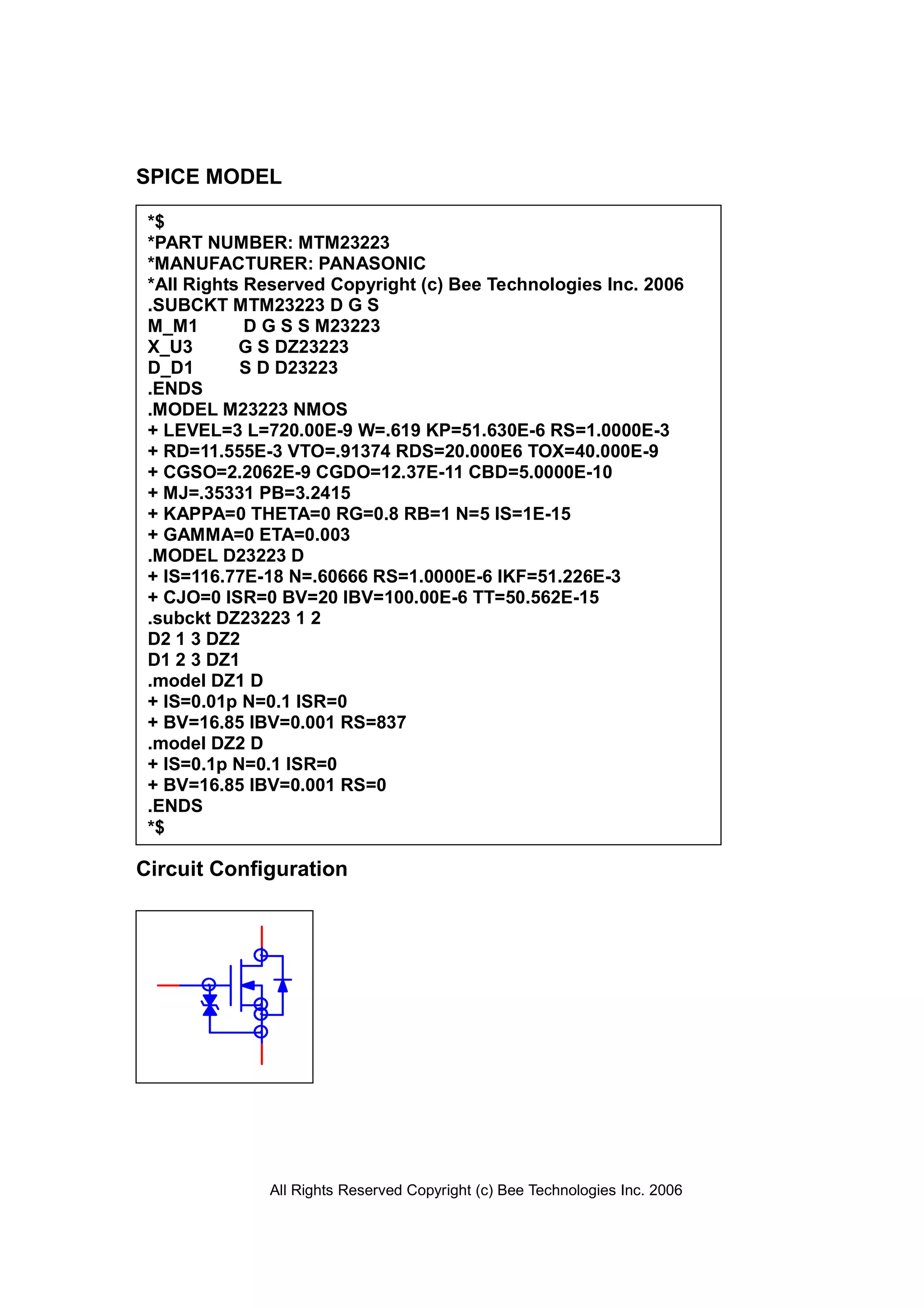
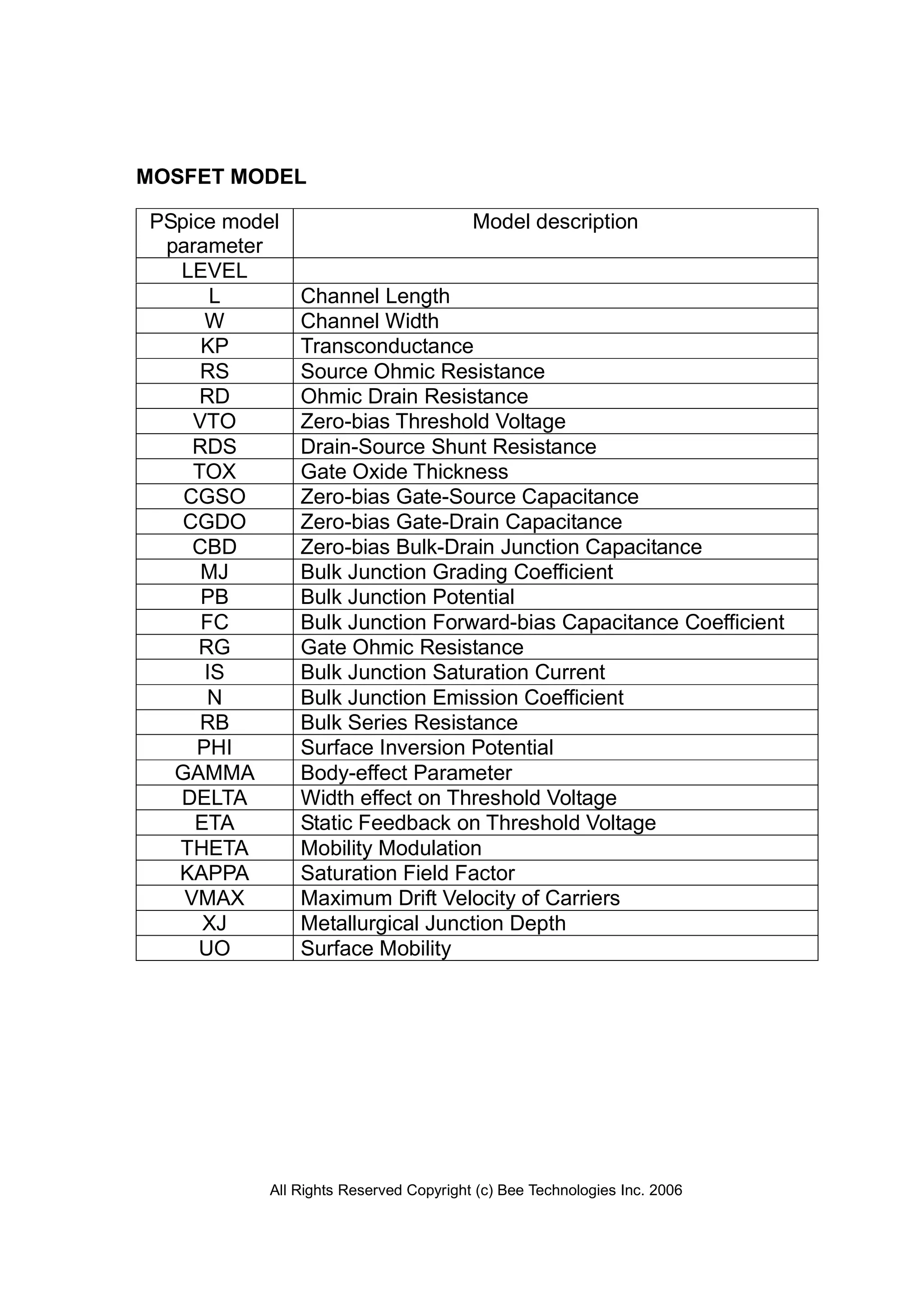
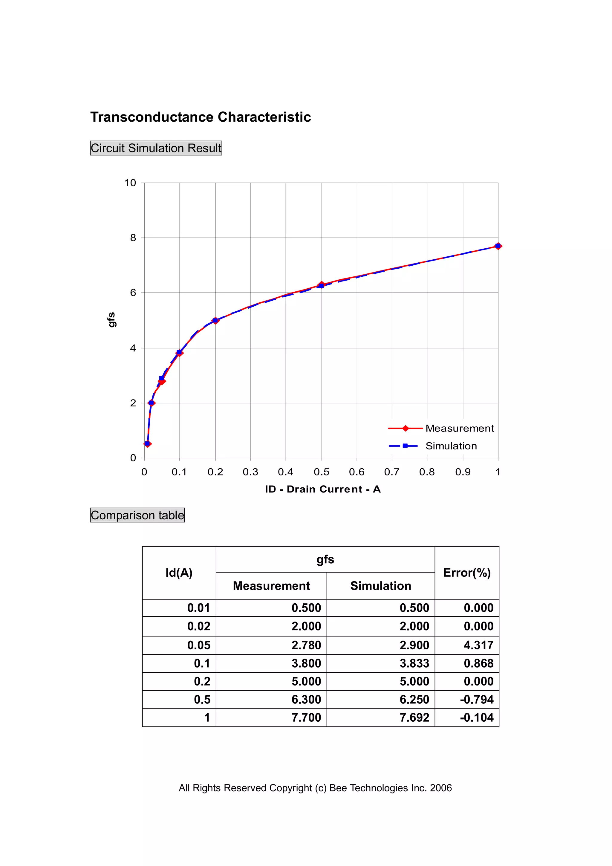
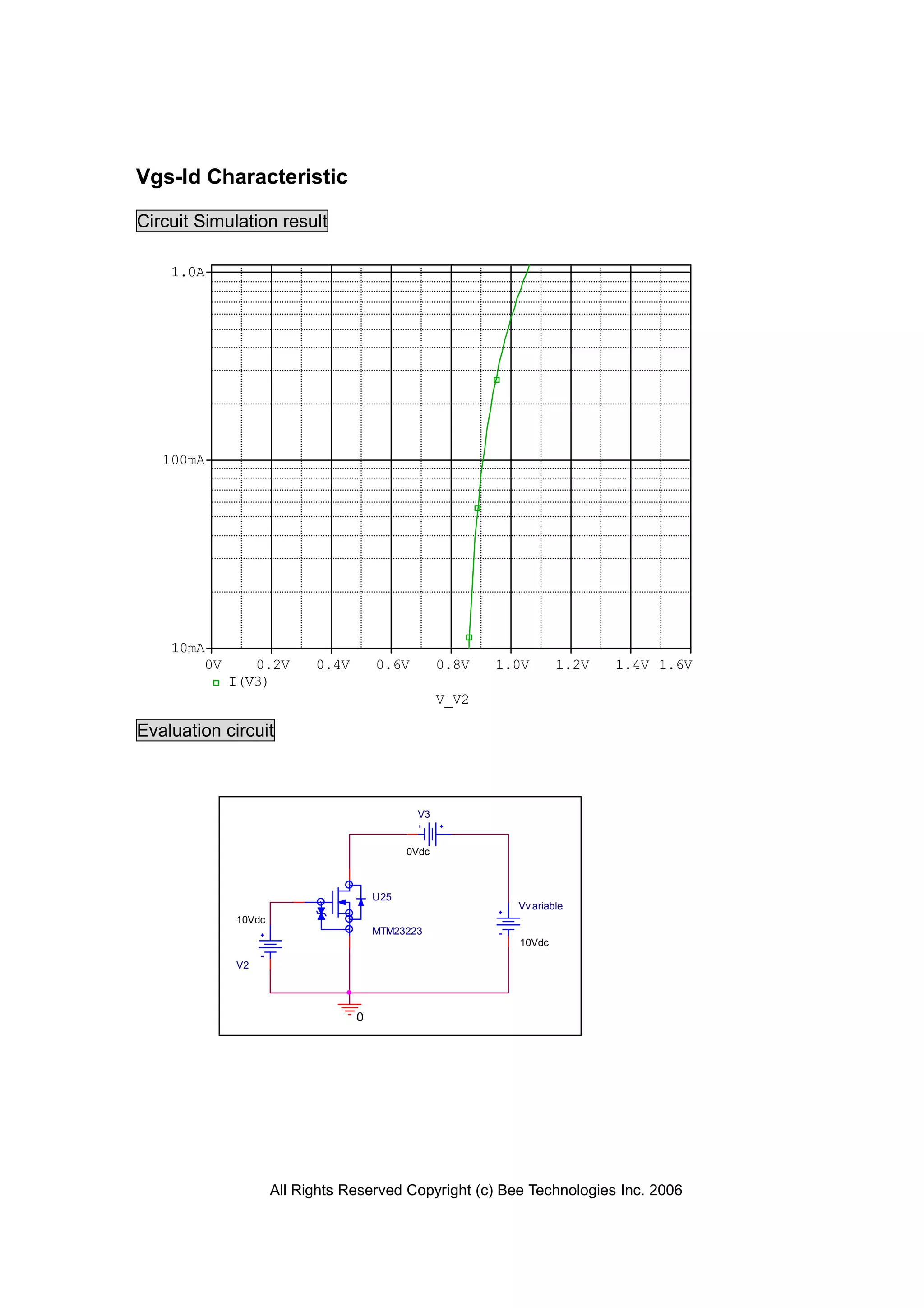
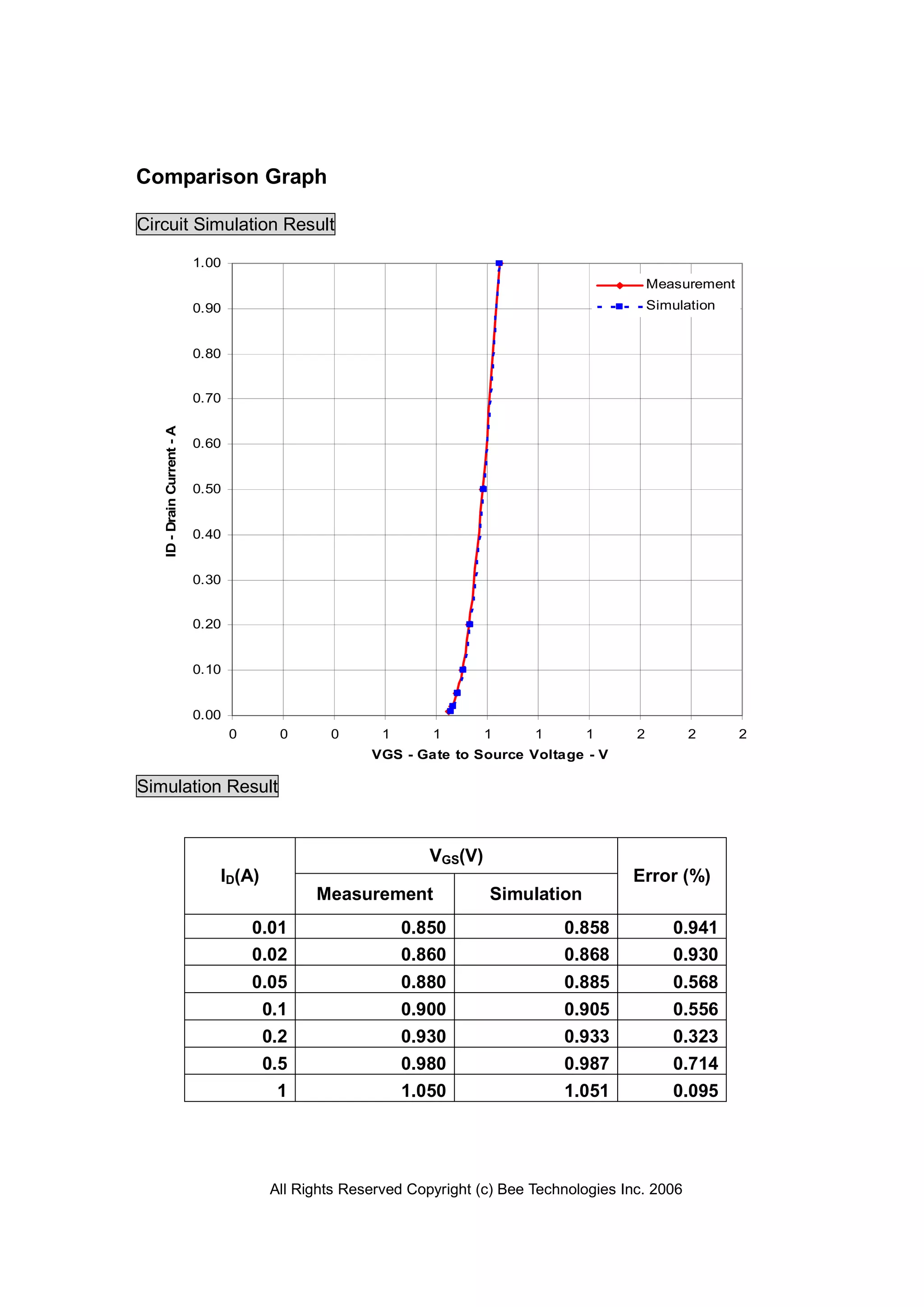
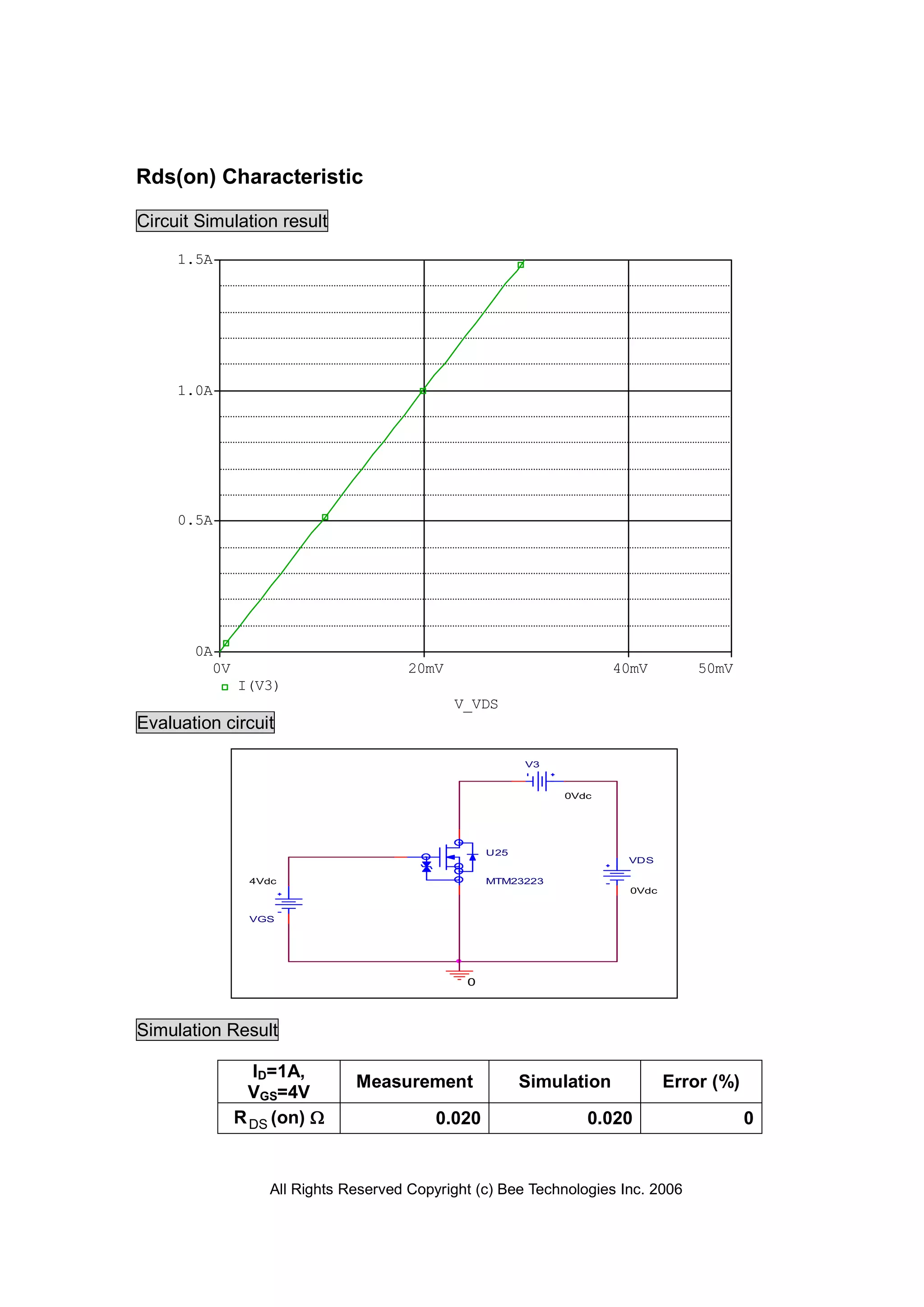
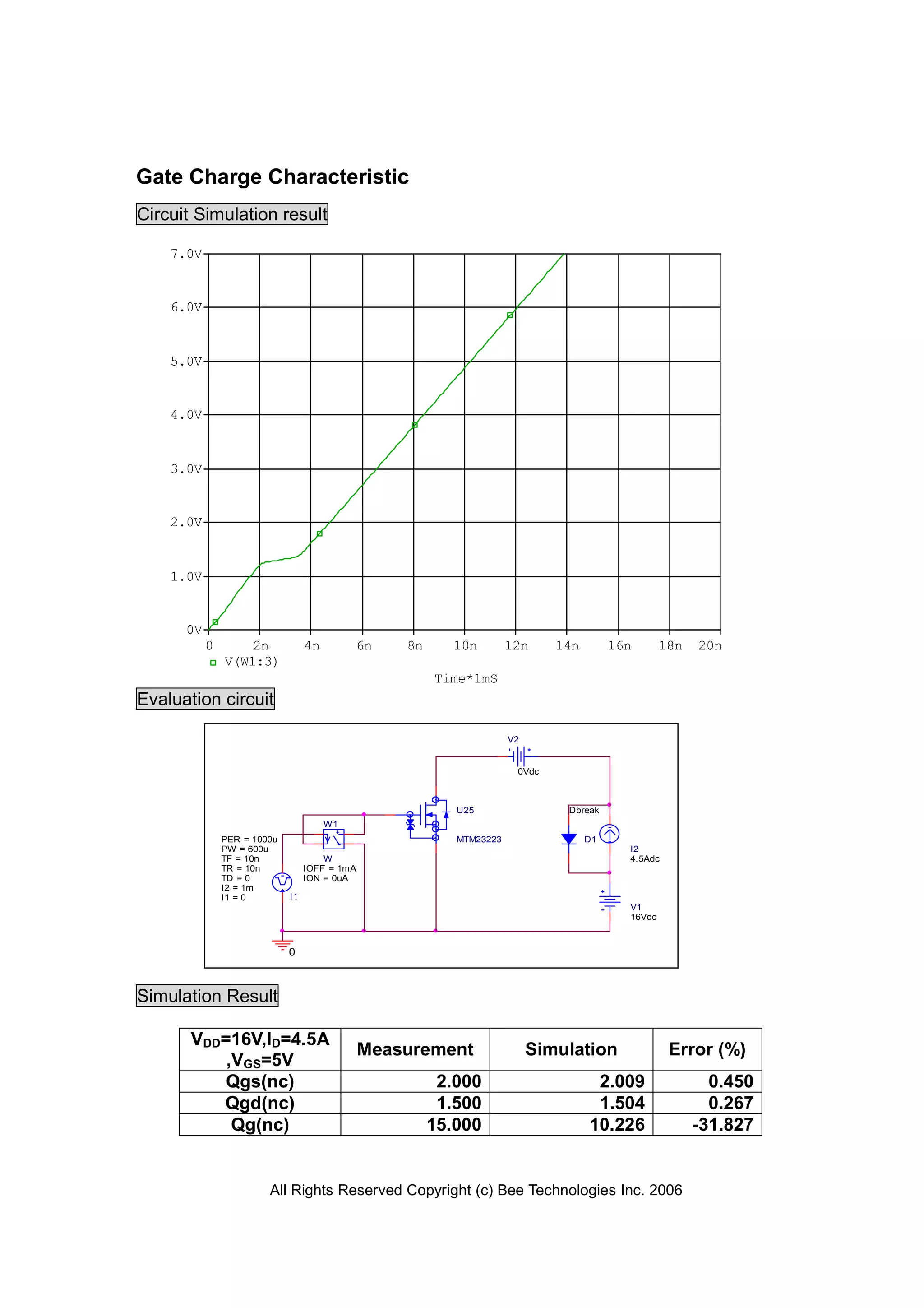
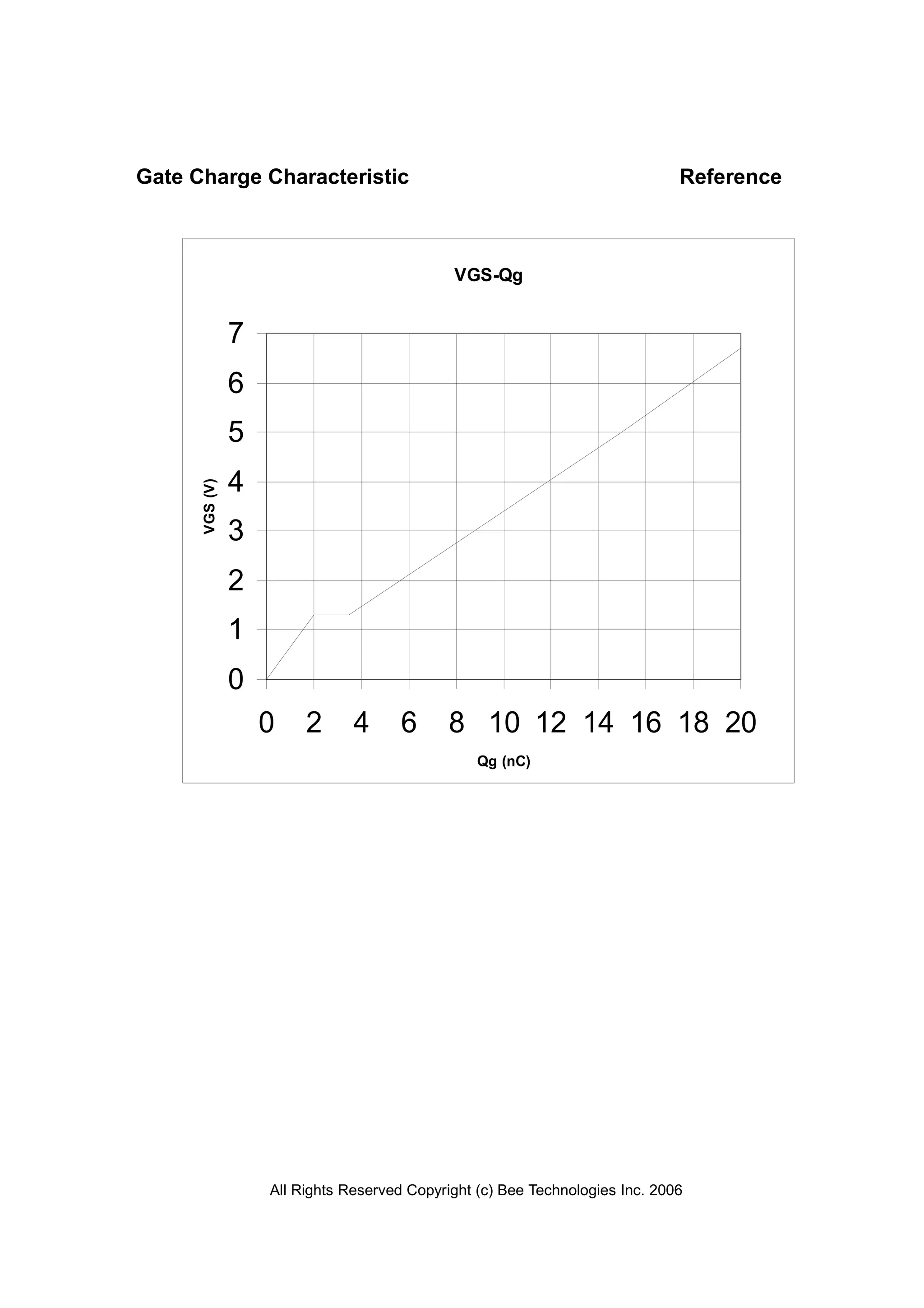
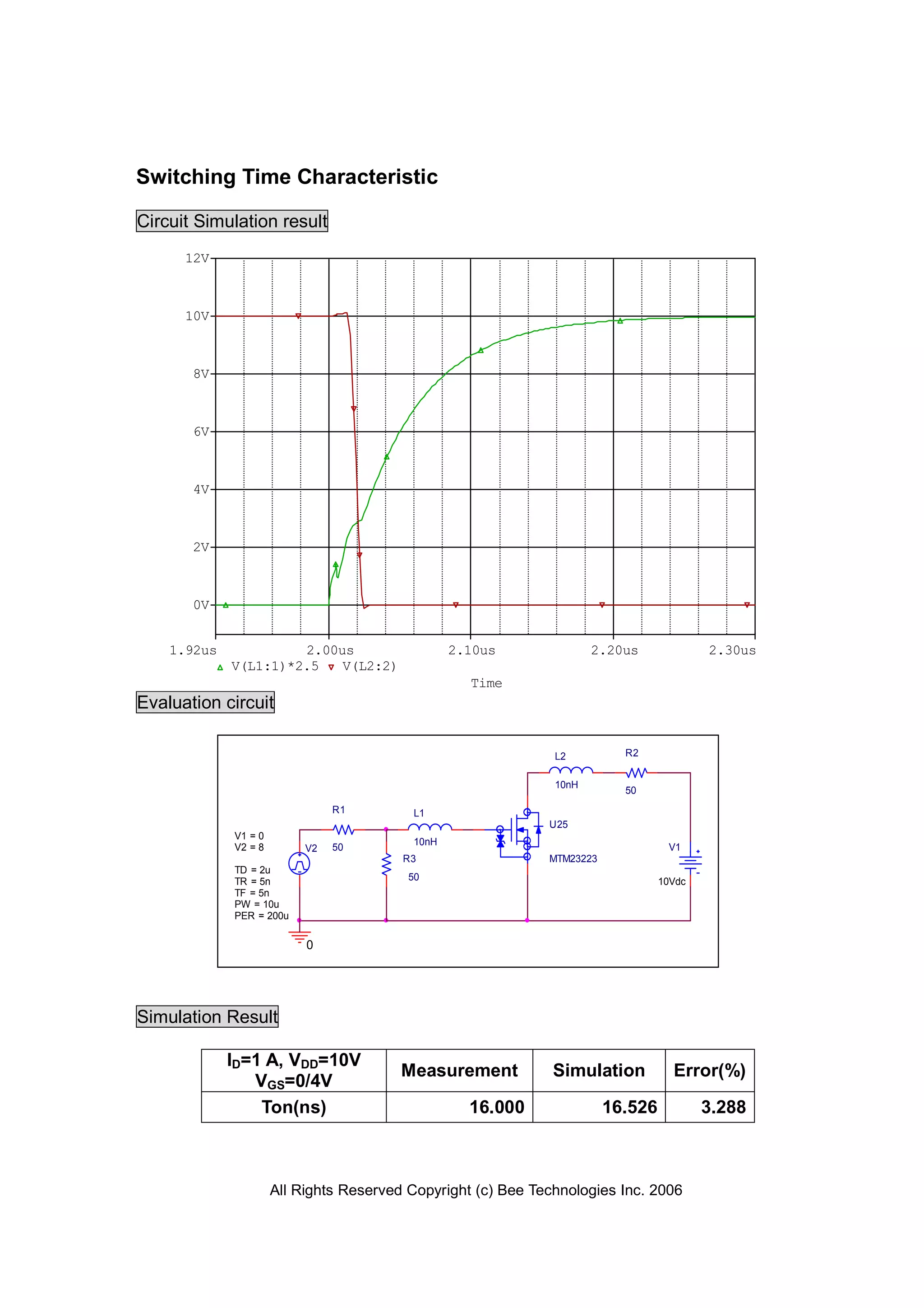
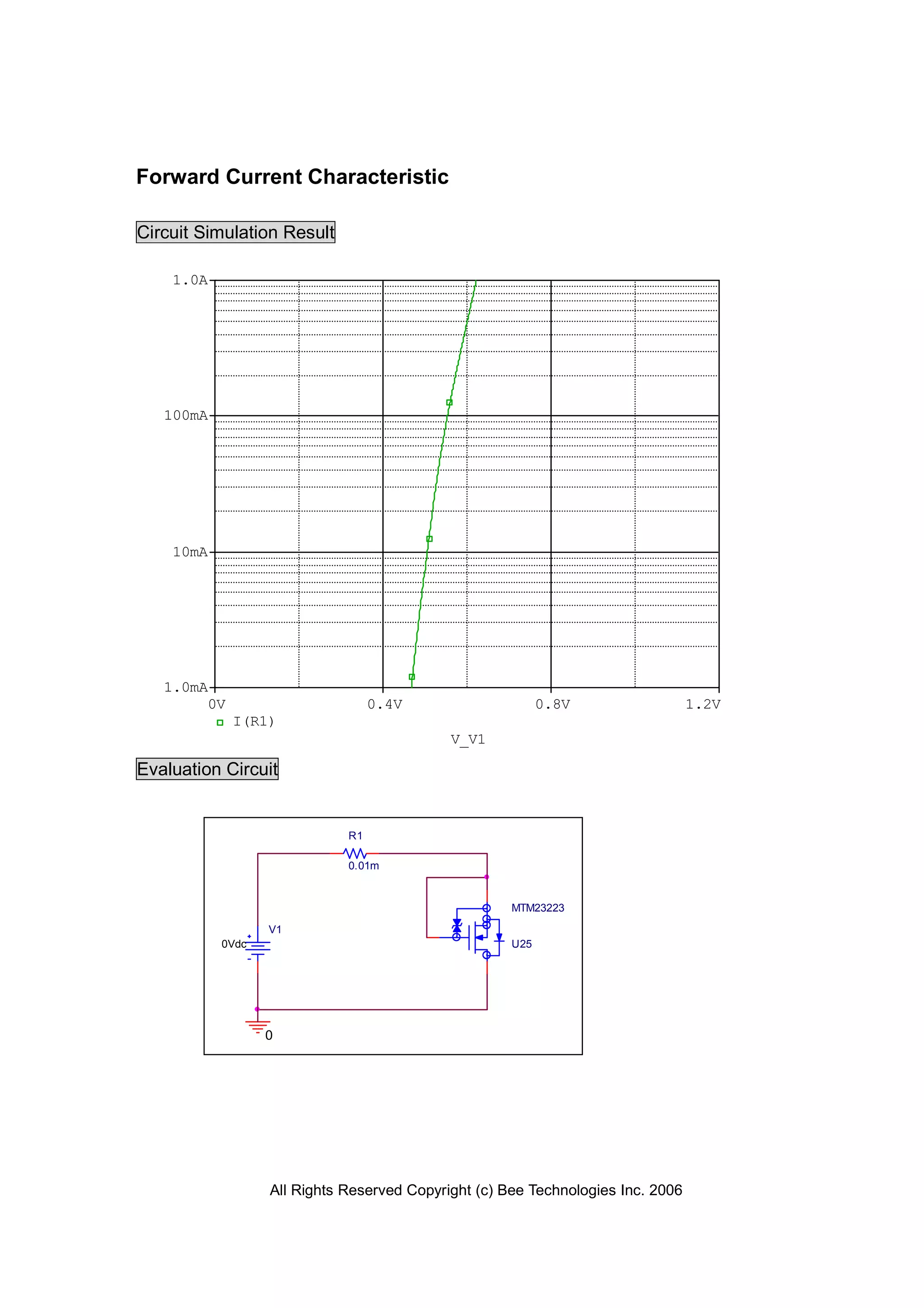
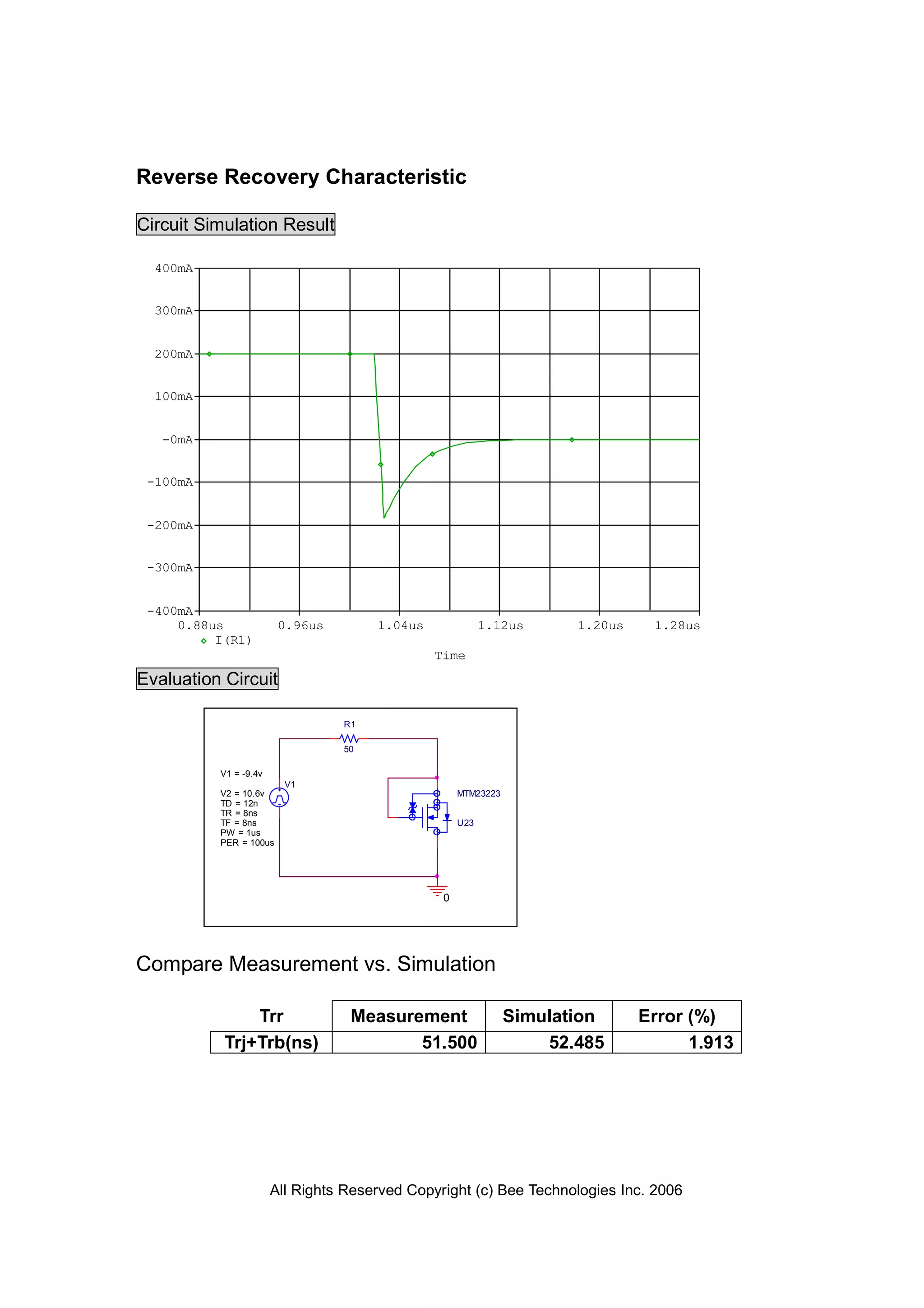
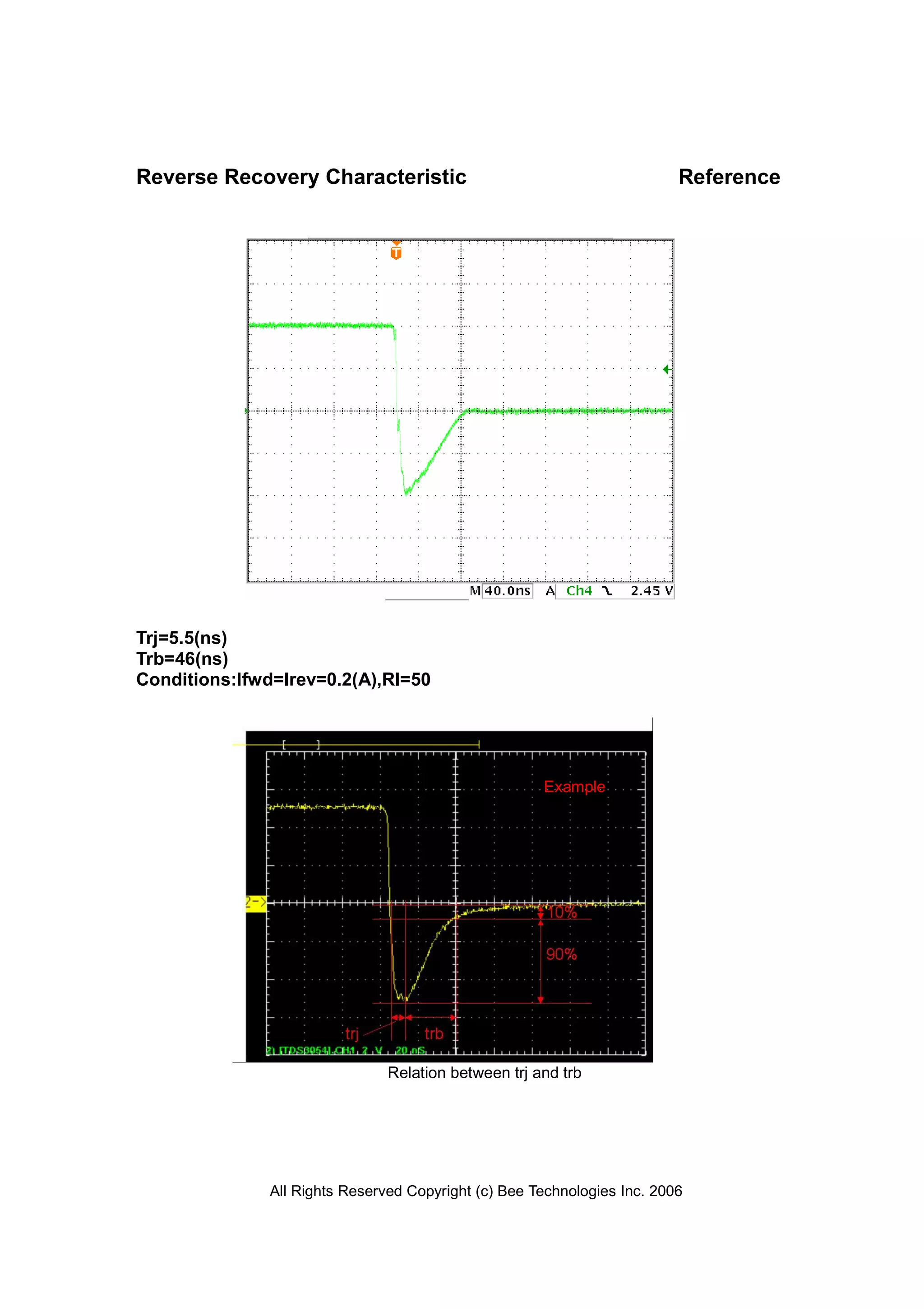
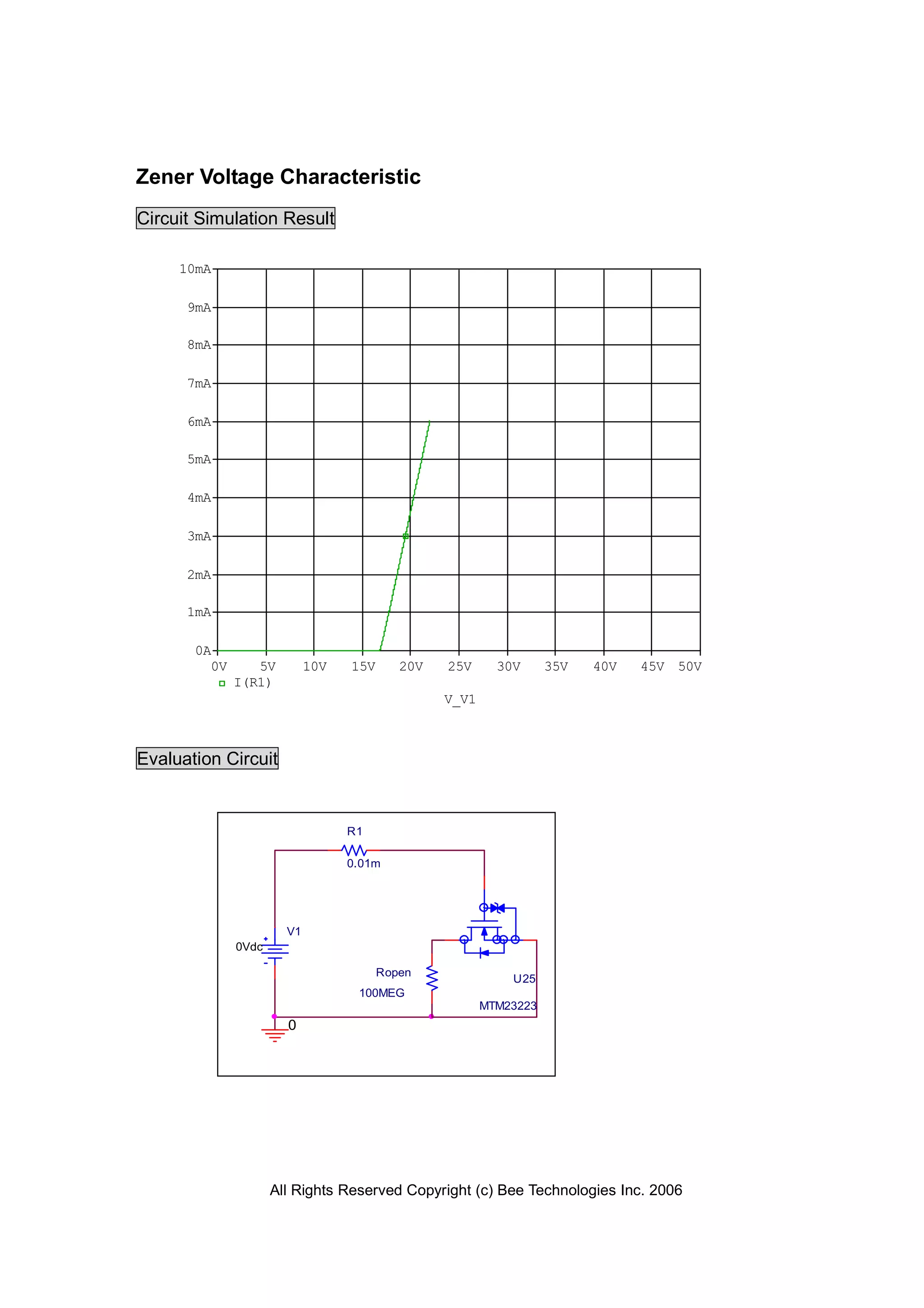
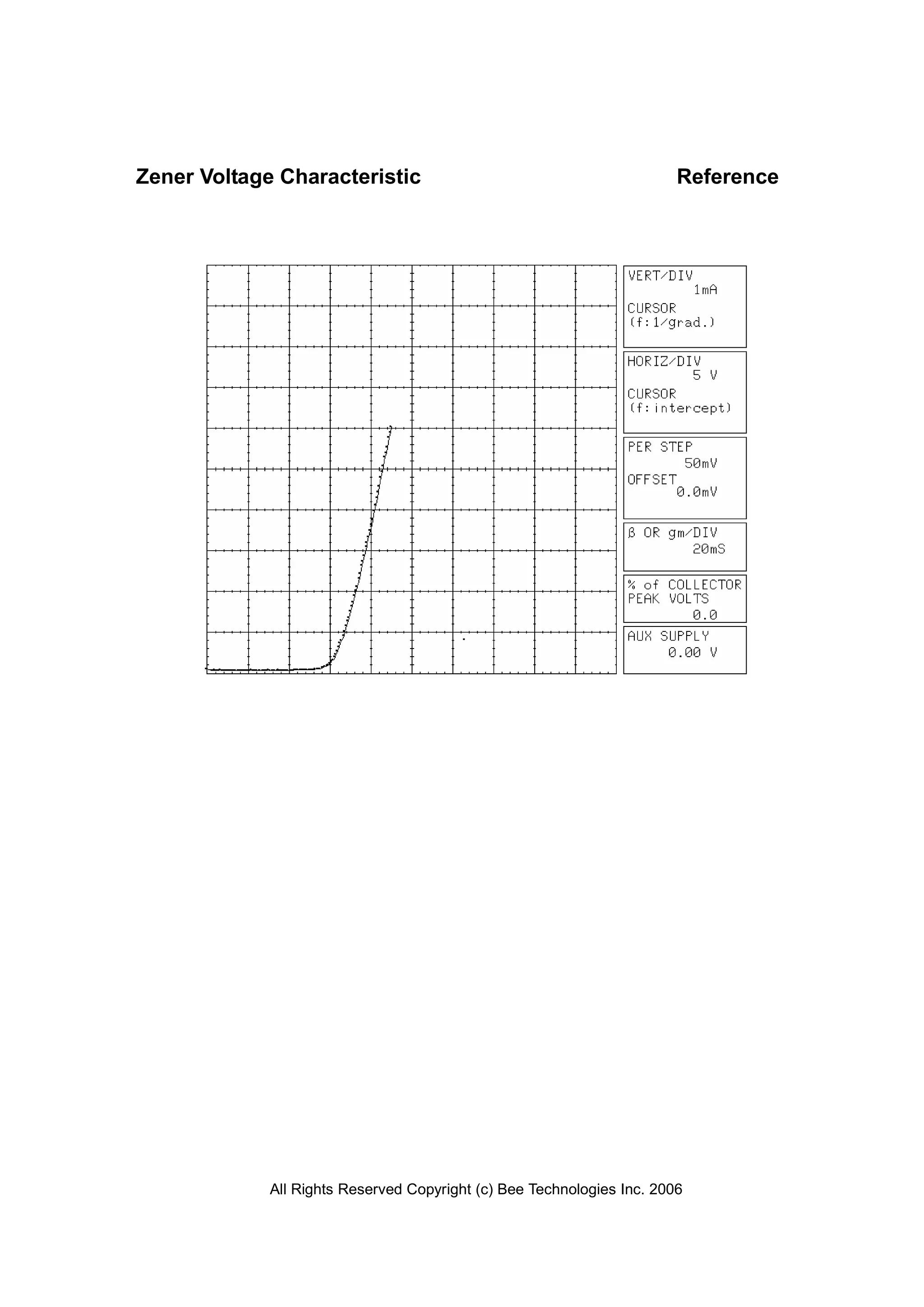
This document provides a summary of simulation results for a MOSFET device model. It includes:
1) A SPICE model for the MTM23223 power MOSFET including parameters for the MOSFET, body diode, and ESD protection diodes.
2) Simulation results graphs for transconductance, Vgs-Id characteristics, Rds(on), gate charge, capacitance characteristics, switching time, output characteristics, and reverse recovery that compare measurements to simulations.
3) Evaluation circuits used in the simulations and tables comparing measurement and simulation results.
Beyond Boundaries: Leveraging No-Code Solutions for Industry Innovation
Bee Technologies MOSFET and Diode Modeling Report
1. All Rights Reserved Copyright (c) Bee Technologies Inc. 2006
Device Modeling Report
Bee Technologies Inc.
COMPONENTS: Power MOSFET (Model Parameters)
PART NUMBER: MTM23223
MANUFACTURER: PANASONIC
Body Diode (Model Parameters) / ESD Protection Diode
2. All Rights Reserved Copyright (c) Bee Technologies Inc. 2006
*$
*PART NUMBER: MTM23223
*MANUFACTURER: PANASONIC
*All Rights Reserved Copyright (c) Bee Technologies Inc. 2006
.SUBCKT MTM23223 D G S
M_M1 D G S S M23223
X_U3 G S DZ23223
D_D1 S D D23223
.ENDS
.MODEL M23223 NMOS
+ LEVEL=3 L=720.00E-9 W=.619 KP=51.630E-6 RS=1.0000E-3
+ RD=11.555E-3 VTO=.91374 RDS=20.000E6 TOX=40.000E-9
+ CGSO=2.2062E-9 CGDO=12.37E-11 CBD=5.0000E-10
+ MJ=.35331 PB=3.2415
+ KAPPA=0 THETA=0 RG=0.8 RB=1 N=5 IS=1E-15
+ GAMMA=0 ETA=0.003
.MODEL D23223 D
+ IS=116.77E-18 N=.60666 RS=1.0000E-6 IKF=51.226E-3
+ CJO=0 ISR=0 BV=20 IBV=100.00E-6 TT=50.562E-15
.subckt DZ23223 1 2
D2 1 3 DZ2
D1 2 3 DZ1
.model DZ1 D
+ IS=0.01p N=0.1 ISR=0
+ BV=16.85 IBV=0.001 RS=837
.model DZ2 D
+ IS=0.1p N=0.1 ISR=0
+ BV=16.85 IBV=0.001 RS=0
.ENDS
*$
SPICE MODEL
Circuit Configuration
3. All Rights Reserved Copyright (c) Bee Technologies Inc. 2006
MOSFET MODEL
PSpice model
parameter
Model description
LEVEL
L Channel Length
W Channel Width
KP Transconductance
RS Source Ohmic Resistance
RD Ohmic Drain Resistance
VTO Zero-bias Threshold Voltage
RDS Drain-Source Shunt Resistance
TOX Gate Oxide Thickness
CGSO Zero-bias Gate-Source Capacitance
CGDO Zero-bias Gate-Drain Capacitance
CBD Zero-bias Bulk-Drain Junction Capacitance
MJ Bulk Junction Grading Coefficient
PB Bulk Junction Potential
FC Bulk Junction Forward-bias Capacitance Coefficient
RG Gate Ohmic Resistance
IS Bulk Junction Saturation Current
N Bulk Junction Emission Coefficient
RB Bulk Series Resistance
PHI Surface Inversion Potential
GAMMA Body-effect Parameter
DELTA Width effect on Threshold Voltage
ETA Static Feedback on Threshold Voltage
THETA Mobility Modulation
KAPPA Saturation Field Factor
VMAX Maximum Drift Velocity of Carriers
XJ Metallurgical Junction Depth
UO Surface Mobility
16. All Rights Reserved Copyright (c) Bee Technologies Inc. 2006
Reverse Recovery Characteristic Reference
Trj=5.5(ns)
Trb=46(ns)
Conditions:Ifwd=lrev=0.2(A),Rl=50
Relation between trj and trb
Example