
Recommended
Recommended
More Related Content
What's hot
What's hot (20)
Similar to Original Power N-Channel MOSFET FR13N15D FR13N15 13N15 150V 14A TO-252 New International Rectifier
Similar to Original Power N-Channel MOSFET FR13N15D FR13N15 13N15 150V 14A TO-252 New International Rectifier (17)
More from AUTHELECTRONIC
More from AUTHELECTRONIC (20)
Recently uploaded
Recently uploaded (20)
Original Power N-Channel MOSFET FR13N15D FR13N15 13N15 150V 14A TO-252 New International Rectifier
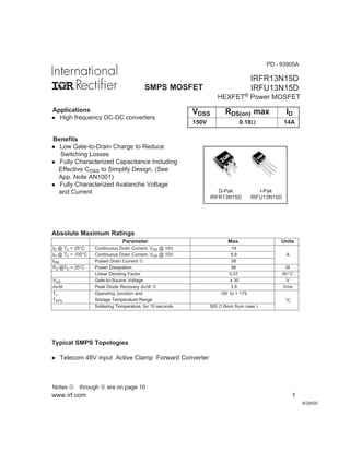
- 1. www.irf.com 1 6/29/00 IRFR13N15D IRFU13N15DSMPS MOSFET HEXFET® Power MOSFET VDSS RDS(on) max ID 150V 0.18Ω 14A Parameter Max. Units ID @ TC = 25°C Continuous Drain Current, VGS @ 10V 14 ID @ TC = 100°C Continuous Drain Current, VGS @ 10V 9.8 A IDM Pulsed Drain Current 56 PD @TC = 25°C Power Dissipation 86 W Linear Derating Factor 0.57 W/°C VGS Gate-to-Source Voltage ± 30 V dv/dt Peak Diode Recovery dv/dt ƒ 3.8 V/ns TJ Operating Junction and -55 to + 175 TSTG Storage Temperature Range Soldering Temperature, for 10 seconds 300 (1.6mm from case ) °C Absolute Maximum Ratings Notes through … are on page 10 D-Pak IRFR13N15D I-Pak IRFU13N15D PD - 93905A l High frequency DC-DC converters Benefits Applications l Low Gate-to-Drain Charge to Reduce Switching Losses l Fully Characterized Capacitance Including Effective COSS to Simplify Design, (See App. Note AN1001) l Fully Characterized Avalanche Voltage and Current Typical SMPS Topologies l Telecom 48V input Active Clamp Forward Converter
- 2. 2 www.irf.com IRFR13N15D/IRFU13N15D Parameter Min. Typ. Max. Units Conditions gfs Forward Transconductance 5.0 ––– ––– S VDS = 50V, ID = 8.3A Qg Total Gate Charge ––– 19 29 ID = 8.3A Qgs Gate-to-Source Charge ––– 5.5 8.2 nC VDS = 120V Qgd Gate-to-Drain ("Miller") Charge ––– 9.4 14 VGS = 10V, „ td(on) Turn-On Delay Time ––– 8.0 ––– VDD = 75V tr Rise Time ––– 26 ––– ID = 8.3A td(off) Turn-Off Delay Time ––– 12 ––– RG = 11Ω tf Fall Time ––– 11 ––– VGS = 10V „ Ciss Input Capacitance ––– 620 ––– VGS = 0V Coss Output Capacitance ––– 130 ––– VDS = 25V Crss Reverse Transfer Capacitance ––– 38 ––– pF ƒ = 1.0MHz Coss Output Capacitance ––– 780 ––– VGS = 0V, VDS = 1.0V, ƒ = 1.0MHz Coss Output Capacitance ––– 62 ––– VGS = 0V, VDS = 120V, ƒ = 1.0MHz Coss eff. Effective Output Capacitance ––– 110 ––– VGS = 0V, VDS = 0V to 120V … Dynamic @ TJ = 25°C (unless otherwise specified) ns Parameter Typ. Max. Units EAS Single Pulse Avalanche Energy‚ ––– 130 mJ IAR Avalanche Current ––– 8.3 A EAR Repetitive Avalanche Energy ––– 8.6 mJ Avalanche Characteristics S D G Parameter Min. Typ. Max. Units Conditions IS Continuous Source Current MOSFET symbol (Body Diode) ––– ––– showing the ISM Pulsed Source Current integral reverse (Body Diode) ––– ––– p-n junction diode. VSD Diode Forward Voltage ––– ––– 1.3 V TJ = 25°C, IS = 8.3A, VGS = 0V „ trr Reverse Recovery Time ––– 110 ––– ns TJ = 25°C, IF = 8.3A Qrr Reverse RecoveryCharge ––– 520 ––– nC di/dt = 100A/µs „ ton Forward Turn-On Time Intrinsic turn-on time is negligible (turn-on is dominated by LS+LD) Diode Characteristics 14 56 A Static @ TJ = 25°C (unless otherwise specified) Parameter Min. Typ. Max. Units Conditions V(BR)DSS Drain-to-Source Breakdown Voltage 150 ––– ––– V VGS = 0V, ID = 250µA ∆V(BR)DSS/∆TJ Breakdown Voltage Temp. Coefficient ––– 0.17 ––– V/°C Reference to 25°C, ID = 1mA † RDS(on) Static Drain-to-Source On-Resistance ––– ––– 0.18 Ω VGS = 10V, ID = 8.3A „ VGS(th) Gate Threshold Voltage 3.0 ––– 5.5 V VDS = VGS, ID = 250µA ––– ––– 25 µA VDS = 150V, VGS = 0V ––– ––– 250 VDS = 120V, VGS = 0V, TJ = 150°C Gate-to-Source Forward Leakage ––– ––– 100 VGS = 30V Gate-to-Source Reverse Leakage ––– ––– -100 nA VGS = -30V IGSS IDSS Drain-to-Source Leakage Current Parameter Typ. Max. Units RθJC Junction-to-Case ––– 1.75 RθJA Junction-to-Ambient (PCB mount)* ––– 50 °C/W RθJA Junction-to-Ambient ––– 110 Thermal Resistance
- 3. www.irf.com 3 IRFR13N15D/IRFU13N15D Fig 4. Normalized On-Resistance Vs. Temperature Fig 2. Typical Output CharacteristicsFig 1. Typical Output Characteristics Fig 3. Typical Transfer Characteristics 0.1 1 10 100 5 6 7 8 9 10 11 V = 50V 20µs PULSE WIDTH DS V , Gate-to-Source Voltage (V) I,Drain-to-SourceCurrent(A) GS D T = 25 CJ ° T = 175 CJ ° -60 -40 -20 0 20 40 60 80 100 120 140 160 180 0.0 0.5 1.0 1.5 2.0 2.5 3.0 T , Junction Temperature ( C) R,Drain-to-SourceOnResistance (Normalized) J DS(on) ° V = I = GS D 10V 14A 0.01 0.1 1 10 100 0.1 1 10 100 20µs PULSE WIDTH T = 25 CJ ° TOP BOTTOM VGS 15V 12V 10V 8.0V 7.0V 6.0V 5.5V 5.0V V , Drain-to-Source Voltage (V) I,Drain-to-SourceCurrent(A) DS D 5.0V 0.1 1 10 100 0.1 1 10 100 20µs PULSE WIDTH T = 175 CJ ° TOP BOTTOM VGS 15V 12V 10V 8.0V 7.0V 6.0V 5.5V 5.0V V , Drain-to-Source Voltage (V) I,Drain-to-SourceCurrent(A) DS D 5.0V
- 4. 4 www.irf.com IRFR13N15D/IRFU13N15D Fig 8. Maximum Safe Operating Area Fig 6. Typical Gate Charge Vs. Gate-to-Source Voltage Fig 5. Typical Capacitance Vs. Drain-to-Source Voltage Fig 7. Typical Source-Drain Diode Forward Voltage 0 5 10 15 20 25 30 0 4 8 12 16 20 Q , Total Gate Charge (nC) V,Gate-to-SourceVoltage(V) G GS FOR TEST CIRCUIT SEE FIGURE I =D 13 8.3A V = 30VDS V = 75VDS V = 120VDS 0.1 1 10 100 0.2 0.4 0.6 0.8 1.0 1.2 1.4 V ,Source-to-Drain Voltage (V) I,ReverseDrainCurrent(A) SD SD V = 0 VGS T = 25 CJ ° T = 175 CJ ° 0.1 1 10 100 1000 1 10 100 1000 OPERATION IN THIS AREA LIMITED BY RDS(on) Single Pulse T T = 175 C = 25 C° °J C V , Drain-to-Source Voltage (V) I,DrainCurrent(A)I,DrainCurrent(A) DS D 10us 100us 1ms 10ms 1 10 100 1000 VDS, Drain-to-Source Voltage (V) 10 100 1000 10000 C,Capacitance(pF) Coss Crss Ciss VGS = 0V, f = 1 MHZ Ciss = Cgs + Cgd, Cds SHORTED Crss = Cgd Coss = Cds + Cgd
- 5. www.irf.com 5 IRFR13N15D/IRFU13N15D Fig 10a. Switching Time Test Circuit VDS 90% 10% VGS td(on) tr td(off) tf Fig 10b. Switching Time Waveforms VDS Pulse Width ≤ 1 µs Duty Factor ≤ 0.1 % RD VGS RG D.U.T. VGS + -VDD Fig 11. Maximum Effective Transient Thermal Impedance, Junction-to-Case Fig 9. Maximum Drain Current Vs. Case Temperature 0.01 0.1 1 10 0.00001 0.0001 0.001 0.01 0.1 Notes: 1. Duty factor D = t / t 2. Peak T = P x Z + T 1 2 J DM thJC C P t t DM 1 2 t , Rectangular Pulse Duration (sec) ThermalResponse(Z) 1 thJC 0.01 0.02 0.05 0.10 0.20 D = 0.50 SINGLE PULSE (THERMAL RESPONSE) 25 50 75 100 125 150 175 0 2 4 6 8 10 12 14 T , Case Temperature ( C) I,DrainCurrent(A) °C D
- 6. 6 www.irf.com IRFR13N15D/IRFU13N15D QG QGS QGD VG Charge D.U.T. VDS IDIG 3mA VGS .3µF 50KΩ .2µF12V Current Regulator Same Type as D.U.T. Current Sampling Resistors + - Fig 13b. Gate Charge Test CircuitFig 13a. Basic Gate Charge Waveform Fig 12c. Maximum Avalanche Energy Vs. Drain Current Fig 12b. Unclamped Inductive Waveforms Fig 12a. Unclamped Inductive Test Circuit tp V(BR)DSS IAS R G IAS 0.01Ωtp D.U.T LVDS + - VD D DRIVER A 15V 20V 25 50 75 100 125 150 175 0 40 80 120 160 200 240 Starting T , Junction Temperature ( C) E,SinglePulseAvalancheEnergy(mJ) J AS ° ID TOP BOTTOM 3.4A 5.9A 8.3A
- 7. www.irf.com 7 IRFR13N15D/IRFU13N15D P.W. Period di/dt Diode Recovery dv/dt Ripple ≤ 5% Body Diode Forward Drop Re-Applied Voltage Reverse Recovery Current Body Diode Forward Current VGS=10V VDD ISD Driver Gate Drive D.U.T. ISD Waveform D.U.T. VDS Waveform Inductor Curent D = P.W. Period + - + + +- - - Fig 14. For N-Channel HEXFET® Power MOSFETs * VGS = 5V for Logic Level Devices Peak Diode Recovery dv/dt Test Circuit ƒ „ ‚ RG VDD • dv/dt controlled by RG • Driver same type as D.U.T. • ISD controlled by Duty Factor "D" • D.U.T. - Device Under Test D.U.T Circuit Layout Considerations • Low Stray Inductance • Ground Plane • Low Leakage Inductance Current Transformer *
- 8. 8 www.irf.com IRFR13N15D/IRFU13N15D D-Pak (TO-252AA) Package Outline Dimensions are shown in millimeters (inches) D-Pak (TO-252AA) Part Marking Information 6.73 (.265) 6.35 (.250) - A - 4 1 2 3 6.22 (.245) 5.97 (.235) - B - 3X 0.89 (.035) 0.64 (.025) 0.25 (.010) M A M B 4.57 (.180) 2.28 (.090) 2X 1.14 (.045) 0.76 (.030) 1.52 (.060) 1.15 (.045) 1.02 (.040) 1.64 (.025) 5.46 (.215) 5.21 (.205) 1.27 (.050) 0.88 (.035) 2.38 (.094) 2.19 (.086) 1.14 (.045) 0.89 (.035) 0.58 (.023) 0.46 (.018) 6.45 (.245) 5.68 (.224) 0.51 (.020) M IN. 0.58 (.023) 0.46 (.018) LE AD A SS IG N M E NTS 1 - GA TE 2 - D R A IN 3 - S OU R CE 4 - D R A IN 10.42 (.410) 9.40 (.370) N OTE S : 1 D IME N S ION IN G & TOLE R A N C IN G P E R A N S I Y 14.5M, 1982. 2 C ON TR OLLING D IM EN SION : IN C H . 3 C ON FO R MS TO JE D E C OU TLIN E TO-252AA . 4 D IME N S ION S SH OW N A R E B EF OR E S OLD ER D IP , S OLD ER D IP M A X. +0.16 (.006).
- 9. www.irf.com 9 IRFR13N15D/IRFU13N15D I-Pak (TO-251AA) Package Outline Dimensions are shown in millimeters (inches) I-Pak (TO-251AA) Part Marking Information 6.73 (.265) 6.35 (.250) - A - 6.22 (.245) 5.97 (.235) - B - 3X 0.89 (.035) 0.64 (.025) 0.25 (.010) M A M B2.28 (.090) 1.14 (.045) 0.76 (.030) 5.46 (.215) 5.21 (.205) 1.27 (.050) 0.88 (.035) 2.38 (.094) 2.19 (.086) 1.14 (.045) 0.89 (.035) 0.58 (.023) 0.46 (.018) LEAD A SSIGN MEN TS 1 - GATE 2 - D RA IN 3 - SOU R C E 4 - D RA IN N OTE S: 1 D IM EN SION IN G & TOLER AN C IN G P ER AN SI Y14.5M , 1982. 2 C ONTR OLLIN G D IM EN SION : IN C H . 3 C ONF OR MS TO JEDE C OUTLINE TO-252AA. 4 D IM EN SION S S HOW N A R E BE FORE SOLDE R D IP, SOLDE R DIP MAX. +0.16 (.006). 9.65 (.380) 8.89 (.350) 2X 3X 2.28 (.090) 1.91 (.075) 1.52 (.060) 1.15 (.045) 4 1 2 3 6.45 (.245) 5.68 (.224) 0.58 (.023) 0.46 (.018)
- 10. 10 www.irf.com IRFR13N15D/IRFU13N15D D-Pak (TO-252AA) Tape & Reel Information Dimensions are shown in millimeters (inches) TR 16.3 ( .641 ) 15.7 ( .619 ) 8.1 ( .318 ) 7.9 ( .312 ) 12.1 ( .476 ) 11.9 ( .469 ) FEED DIRECTION FEED DIRECTION 16.3 ( .641 ) 15.7 ( .619 ) TRR TRL NOTES : 1. CONTROLLING DIMENSION : MILLIMETER. 2. ALL DIMENSIONS ARE SHOW N IN MILLIMETERS ( INCHES ). 3. OUTLINE CONFO RMS TO EIA-481 & EIA-541. NO TES : 1. OUTLINE CONFORMS TO EIA-481. 16 mm 13 INCH IR WORLD HEADQUARTERS: 233 Kansas St., El Segundo, California 90245, USA Tel: (310) 252-7105 IR EUROPEAN REGIONAL CENTRE: 439/445 Godstone Rd, Whyteleafe, Surrey CR3 OBL, UK Tel: ++ 44 (0)20 8645 8000 IR CANADA: 15 Lincoln Court, Brampton, Ontario L6T3Z2, Tel: (905) 453 2200 IR GERMANY: Saalburgstrasse 157, 61350 Bad Homburg Tel: ++ 49 (0) 6172 96590 IR ITALY: Via Liguria 49, 10071 Borgaro, Torino Tel: ++ 39 011 451 0111 IR JAPAN: K&H Bldg., 2F, 30-4 Nishi-Ikebukuro 3-Chome, Toshima-Ku, Tokyo 171 Tel: 81 (0)3 3983 0086 IR SOUTHEAST ASIA: 1 Kim Seng Promenade, Great World City West Tower, 13-11, Singapore 237994 Tel: ++ 65 (0)838 4630 IR TAIWAN:16 Fl. Suite D. 207, Sec. 2, Tun Haw South Road, Taipei, 10673 Tel: 886-(0)2 2377 9936 Data and specifications subject to change without notice. 6/00 Repetitive rating; pulse width limited by max. junction temperature. ƒ ISD ≤ 8.3A, di/dt ≤ 280A/µs, VDD ≤ V(BR)DSS, TJ ≤ 175°C Notes: ‚ Starting TJ = 25°C, L = 3.8mH RG = 25Ω, IAS = 8.3A. „ Pulse width ≤ 300µs; duty cycle ≤ 2%. … Coss eff. is a fixed capacitance that gives the same charging time as Coss while VDS is rising from 0 to 80% VDSS * When mounted on 1" square PCB (FR-4 or G-10 Material). For recommended footprint and soldering techniques refer to application note #AN-994.