SlideShare a Scribd company logo
1 of 54
+
-
VB
+
-
VC
+
-
VA
IC
IB
IA
ID
= - ( IA
+ IB
+ IC
)
1
2
3
4
Use terminal 1 as a reference to define
terminal voltages and currents
In general:
 
C
B
A
A
A v
,
v
,
v
f
i 
 
C
B
A
B
B v
,
v
,
v
f
i 
 
C
B
A
C
C v
,
v
,
v
f
i   Large signal nonlinear device (system)
equations may be dependent on range
of voltages and currents.
GENERALIZATION OF SMALL SIGNALAPPOXIMATION TO MULTITERMINAL DEVICES
       
     
   












































B
A
Q
B
A
A
C
Q
C
A
B
Q
B
A
A
Q
A
A
C
Q
C
A
B
Q
B
A
A
Q
A
A
C
B
A
A
A
V
v
V
v
v
v
f
V
v
v
f
V
v
v
f
V
v
v
f
V
v
v
f
V
v
v
f
V
v
v
f
V
,
V
,
V
f
i
B
A
2
C
2
2
2
B
2
2
2
A
2
2
C
B
A
2
1
Taylor series expansion of iA w.r.t. Q point: VA, VB, VC
if |va|, |vb|, |vC| are small enough



 



 

)
t
(
i
c
ac
b
ab
a
aa
A
A
a
v
g
v
g
v
g
I
i 



where
Q
A
A
aa
aa
v
f
r
ˆ
g




1
Q
B
A
ab
v
i
ˆ
g



Q
C
A
ac
v
i
ˆ
g



c
ac
b
ab
a
a
a v
g
v
g
v
g
i 


c
bc
b
b
a
ba
b v
g
v
g
v
g
i 


c
c
b
cb
a
ca
c v
g
v
g
v
g
i 


Small signal analysis for a 4 terminal device
aa
g
a
r 1
 b
abv
g c
acv
g
ia1
ia2
ia3
va
+
-
ia
b
abv
g c
acv
g
ra
va
+
-
ia
vb
+
-
ib
vc
+
-
ic
c
bcv
g rb
a
bav
g b
cbv
g rc
a
cav
g
1
2
3 4
MOST GENERAL SMALL SIGNAL EQUIVALENT CIRCUIT FOR A 4 TERMINAL DEVICE
Remarks:
- All small signal parameters are Q-point dependent.
- Capacitances between terminals have to be considered for high frequency
analysis.
- BJT and MOS are four terminal devices, only a few parameters have non
negligible values.
- Voltage controlled sources indicate how what happens at one port affects
another port (coupling between ports).
E B
VSS
C S
p+
p-substrate
n+
n-
p
n+
n+
b
abv
g c
acv
g
ra
va
+
-
ia
vb
+
-
ib
vc
+
-
ic
c
bcv
g rb
a
bav
g b
cbv
g rc
a
cav
g
1
2
3 4
c
c
cc s
base
gate
emitter
source
collector
drain
substrate
substrate
BJT MODELLING
c ro

v
gm
e
b
S
r
rb
cc s
c
r
rc
c
b´
v
+
-
e´
c´
BJT MODELLING: HYBRID  MODEL
Models leakage current
Substrate
Always connected to “signal”
ground (DC voltage).









 
A
CE
3
V
V
1
T
V
BE
V
e
I
i
i S
c


C
E
C
B
i
i
or
i
i
i 


1
 
C
B
E i
i
i 


 Large signal equations
forward active mode.
C: Forward biased base emitter junction:
 
33
0
VT
f
e
0
1
.
I
where c
V
je
e
oe
EB
c
c 








C: Reversed biased base collector junction:
 
5
0
C
0
1
.
where
C
oc
BC
V
c
c 

 




CCS: Reversed biased collector substrate junction:
 
5
0
1
0
.
where S
V
CS
CS S
oS
CS
c
c 

 


Large area
low doping
r: base emitter resistance:
























 K
.
I
V
Q
C
T
Q
BE
C
Q
BE
B
v
i
v
i
r 5
2
-1
-1



ro: output resistance:













 K
I
V
Q
C
A
Q
CE
C
o
v
i
r 00
1
-1
gm: transconductance:
V
mA
T
BE
C
m
V
I Q
C
v
i
g 0
4





cj0, j0, , F are different for each junction, must be known.
r = 5  r0  100 M can be usually neglected.
re  5  strongly geometry dependent
rb  200  strongly geometry dependent
rc  200 
 Ic dependent
EXAMPLE:
Emitter area 500 m2, High voltage NPN device
VEB0 = 7 V
Cje0 = 1 pF
joe = 0.7 V
e = 0.33
VCB0 = 50 V
C0 = 0.3 pF
joc = 0.7 V
c = 0.5
VCS0 = 70 V
CCS0 = 3 pF
joS = 0.52 V
S = 0.5
SMALL SIGNALANALYSIS
- Set all signal sources to zero.
1.- Perform DC Analysis - Determine all DC voltages and currents if possible
using DC equivalent circuits.
Check for |VCE| > 0.2 V I BJT´s.

- Small signal device parameters can only be
determined if DC(Q ) operating point is known.
3.- Replace devices by small - For small frequency analysis do not include parasitic
signal equivalent circuits device capacitances.
-Small signal equivalent circuits do not depend on the
type of transistor (NPN, PNP).
- Voltage sources short circuits
2.- Passivate DC Sources
- Current sources open circuits


vS
vout
15 K
Q3
Q1
Q2
IBIAS1
1mA
IBIAS2
5mA
3 K
+ 15 V
- 15 V
- 15 V
IB1
vout
15 K
0.7 V
3 K
+ 15 V
- 15 V
- 15 V
0.7 V
0.7 V
IB3
IB2
 IB1
 IB2
 IB1  IB3
ro
EXAMPLE
Since We have the same VBE for Q1 and Q2:
DC
V
V
V
.
V
V
V
.
V
V
.
V
V
m
I
I
where
m
.
I
I
I
C
C
E
C
E
E
BIAS
C
BIAS
C
C
0
mA
5
k
3
15
.2
8
7
0
5
7
mA
0.5
k
15
-
5
1
7
0
-
A
5
1
A
5
0
2
3
2
3
2
2
1
3
2
1
2
1
























All transistors are in active mode.
V
V
V
-
V
V
-
V
EC
CE
CE
.2
8
0
.2
8
.9
8
)
0.7
-
(
8.2
7
15.
)
0.7
-
(
5
1
3
2
1







Calculation of small signal parameters:  = 200, VA= 100 V



















K
I
V
r
K
I
V
r
r
K
I
V
r
r
V
I
g
V
I
g
g
Q
C
A
o
Q
C
A
o
o
Q
C
T
m
T
Q
C
m
m
T
Q
C
m
m
20
mA
5
V
100
0
0
2
mA
0.5
V
100
10
mA
0.5
mV
26
200
200
20
3
2
,
1
2
,
1
3
3
2
1
2
1
V
A
3
V
A
2
1




ro


v
g
i
m
b
e
b
r
c
v
+
-
re
ro
e
i

e
b
c
SIMPLIFIED SMALL SIGNAL EQUIVALENT CIRCUITS FOR BJT´S
m
g
r

 
m
e
e
e
g
i
v
r



e
r
(β
r )
1



ro3
rc3
=3 k
ro1
1
1 
v
gm
b1
r v
+
-
e1
ro2 2
2 
v
gm
r
v
+
-
rc2
=15 K
c1
e2
c2
b2
3
3 
v
gm
r v
+
-
b3
c3
e3
vS
rS 1
2
3
4
5
g1+ Gs
- g1
- g1
g1+ g1+ go1+ g02
- g02
GC2+ go1+ g3
- g02 - g3
- g3 go3
+ g3
- go3
go3
+ GC3
- go3
0
0
0
0
0
0
0
0
0
0
0
0
Gs VS
gm1v1+ gm2v2
- gm2v2
- gm2
v2
+ gm3
v3
- gm3
v3
1 2 3 4 5
1
2
3
4
5
SISTEMATIC PROCEDURE TO WRITE NODALADMITANCE MATRIX:
g1
+ Gs
- g1
- g1
g1+ g1+ go1+ g02
+ gm1
+ gm2
- g02
GC2+ go1+ g3
- g02
- gm2
- g3
- g3
-gm3
go3+ g3+
gm4
- go3
go3+ GC3
- go3
-gm4
0
0
0
0
0
0
0
0
0
0
0
gm3
Gs VS
gm1v1+ gm2v2
- gm2v2
- gm2v2+ gm3v3
- gm3v3
1 2 3 4 5
1
2
3
4
5
ro3
rc3
=3 k
ro1
1
1 
v
gm
b1 r
v
+
-
e1
ro2 2
2 
v
gm
r
v
+
-
rc2
=15 K
c1
e2
c2
b2
3
3 
v
gm
r
v
+
-
b3
c3
e3
vS
rS 1
2
3
4
5
c
c
c
c
c
c
cS3
cS2
g1+ Gs+
s c1 +
s c1
- g1
- g1-
s c1
g1+ g1+ go1+ g02
+ gm1
+ gm2
+s C2
- g02
GC2+ go1+ g3+
s CS
+ s c2
+s c 3
- g02
- gm2
- g3
- s c3
- g3 - gm3
- s c 3
go3+ g3+
gm4
+s c 3
- go3
go3+ GC3+
s c3
+s cS3
- go3
-gm4
0
0
0
- s c3
0
0
0
0
0
0
0
gm3 +
s c3
Gs VS
gm1v1+ gm2v2
- gm2v2
- gm2v2+ gm3v3
- gm3v3
1 2 3 4 5
1
2
3
4
5
B
Substrate
D
Drain
IS
ID
IB
IG
S
Source
Dependent Independent
B
G
S
D i
,
i
,
i
,
i
D
S i
i 

0

G
i
Large signal equations:
BS
DS
S
G v
,
v
,
v
0

B
i
 Only one equation needed
MOS TRANSISTOR (ENHANCEMENT)
Saturated Mode:  
1 BS
DS
GS
D v
,
v
,
v
f
i 
Cutoff Mode: 0

D
i
Nonsaturated Mode:
or triode
 
2 BS
DS
GS
D v
,
v
,
v
f
i 
Weak inversion:
or Subthreshold
 
3 BS
DS
GS
D v
,
v
,
v
f
i 
Strong inversion:
T
GS
DS
T
GD
T
GS
V
V
V
V
V
V
V





MOS TRANSISTOR: OPERATION REGIONS
p-
substrate
n+ n+ p+
G S
D
MOS TRANSISTOR:STRUCTURE.
MOS TRANSISTOR: LARGE SIGNAL EQUATIONS.
Saturated Mode:  
1 BS
DS
GS
D v
,
v
,
v
f
i 
kp transconductance parameter ~
T
GS
DS
T
GD
T
GS V
V
V
or
V
V
V
V 



 
-
)
(
1
1
2
2
L
W
T
GS
DS
T
GS
p
D V
V
v
V
v
k
i 





25 A/V2 n-channel
10 A/V2 p-channel
  V
V
1.6
-
0.8
~
2
2 BS
f e
arg
for l
V
V
V f
BS
to
t j
j
 



Body effect parameter:
1
5
0 
V
.
~

Fermi level: V
.
~ 3
0
f
j
Mobility degradation: m
for
V
.
~ 
 2
L
35
0 1


Channel length modulation: m
3
L
or
3
0 
 
f
.
~
For long dimensions ( L > 3 m ) and Low vGS ( | vGS| < 2 V
     
BS
DS
GS
t
GS
p
D v
,
v
,
v
f
v
V
v
k
i 1
2
DS
2



 
 
T
Q
GS
GS V
V
V 

 is not significant no degradation
   
GS
t
GS
p
D v
f
V
v
k
i
2
2



Used for quick hand calculations: simplified small equivalent circuits.
Used to derive general small equivalent circuits
Condition for small signal approximations
cg s
ro
gs
mv
g
s
cg d
g
vg s
+
-

v
gm
vd s
+
-
vb s
+
-
cd b
cb s
d b
   
Q
t
Q
GS
Q
D
L
W
p
Q
D
Q
t
Q
GS
p
Q
GS
D
m
V
V
I
I
V
L
W
k
V
k
v
i
g








2
2
Output resistance:
D
A
I
V
1
-1












 Q
n
Q
DS
D
o
I
v
i
r

Transconductance:
m
L
W
p
Q
D
Q
BS
D
mb g
I k
v
i
g
2





Body effect bulk transconductance gain
p- substrate
n+ n+ p+
-
-
-
-
-
B
D
G
S
VGS < Vt
VDS
-No current flows, electrons begin to accumulate under gate.
-Strictly speaking: small current flows (subthreshold or weak inversion
operation.
0
0 t
GS
DS V
V
V 


p- substrate
n+ n+ p+
B
D
G
S
VGS > Vt
VDS
- - - - -
-
-
- -
-Channel is induced for vGS ≥ Vt
-The width of the channel is uniform, and is controlled by vGS - Vt.
- For small vDS:
  DS
ox
n
DS
channel L
W
C
R
1
v
V
v
v
i t
GS
D 

 
p- substrate
n+ n+ p+
B
D
G
S
VGS > Vt
VDS
- - - - -
-
-
- -
-
-
- -
-
- vDS > 0 subject to:
vGS > Vt , vGD > Vt
vDS < vGS -Vt (small VDS!)
-Nonuniform channel width, narrower in drain side than in source side:
nonlinear resistive behavior.
 
 
  DS
t
DS
DS
ox
n
-
V
2
-
/2
L
2
W
L
W
C
v
v
v
v
V
v
v
i
DS
GS
p
t
GS
D
k




 
Equation for
triode mode
p- substrate
n+ n+ p+
B
D
G
S
VGS
VDS
- -
-
-
- - -
-
- -
-
- vDS > 0 subject to:
vGS > Vt , vGD < Vt
vDS > vGS -Vt (large VDS!)
-Channel pinch-off: channel width becomes zero on drain size.
- Further increases in vDS once channel pinch-off takes place do not affect.
 2
t
V
L
2
W

 GS
p
D v
i
k
-Large vDS ,
vDS > vGS -Vt
Saturation
mode
Drain terminal performs as high
impedance source depending only
on vDS
-Smal vDS ,
vDS < vGS -Vt
Triode mode Device acts as a voltage controlled
resistor
- Equations are valid for long channel devices !!!!!
REMARKS.
The behavior of short-channel transistors (sub-micron channel length) deviate
from that of the long-channel transistors.
A MOS transistor is called short channel device if its channel length is of the
same order of magnitude as the depletion region thickness of the source and
drain junctions.
Alternatively, a MOSFET transistor can be defined as a short-channel device if
the effective length
 
d
D
eff x
L
L 

 2
is approximately equal to the source and drain junction depth j
x
MOSFETs – Short channel effects
tox
n+ n+
Cross section
L
Gate oxide
xj
The short channel effects that arises in this case are attributed to two
physical phenomena:
(i) The limitation imposed on electron drift characteristics in
the channel, and
(ii) the modification of the threshold voltage due to shortening
channel length.
MOSFETs – Short channel effects
Fundamental scaling limits for conventional MOS devices
MOSFETs – Short channel effects
– Mobility Degradation
• Transistors with channel lengths < 1um
• High gate voltage
• Large electric fields, no longer one-dimensional
• Greater channel depth
• More electron collisions
• Carrier mobility n degraded
• Carrier velocity between source & drain saturates
• Channel’s effective sheet resistance goes up
• How can we model mobility degradation?
• Use finite series source resistance Rsx:
• Rsx = (1/Ec) (1/ nCox) (1/W)
• where Ec = critical electric field ~ 1.5X1E6 v/m
MOSFETs – Short channel effects
– Mobility Degradation
For 0.8m long transistor with nCox = 90 /V2,
Rsx = 6K/m width - much larger than physical source resistance
Id/Vgs square law no longer true - relationship somewhere between
linear and square law
MOSFETs – Short channel effects
Threshold Variations
VT
L
Long-channel threshold LowVDS threshold
Threshold as a function of
the length (for low
VDS)
Drain-induced barrier lowering
(for lowL)
VDS
VT
MOSFETs – Short channel effects
Velocity Saturation
– In long channel devices, the drift velocity of the carriers, vd, is
proportional to the electric field, independent of the value of the field,
Ex. Note that the lateral (horizontal) electric field, along the channel
increases, as the effective channel length decreases.
– For channel electric field of Ex ≥ 105 V/cm, the electron drift velocity in
the channel reaches a saturation value of vd = 105 V/sec. In this case, the
carriers fail to follow the linear model. The critical value of the electric
field at which the carrier velocity saturates, EC, depends on the doping
levels and the vertical electrical field applied (The vertical electric field
is due the voltage applied on the gate of the MOSFET).
eff
DS
d
L
v
v




E
vd



c
d
E
E
E
v
/
1





MOSFETs – Short channel effects
Velocity Saturation
The velocity saturation has very significant implications upon the current-voltage
characteristics of the short-channel MOSFET, especially the n-type
MOSFET. For short-channel, these implications include:
1. Due to carrier velocity saturation, the delivered saturation-mode
current is less than the current value predicted by the conventional
long-channel current equation. The current is no longer a quadratic
function of the gate-to-source voltage,, and it is virtually independent of
the channel length. The saturation current displays a linear
dependence with respect to.
2. The device enters saturation before reaches, i.e., .
3. The actual threshold voltage of the short-channel devices is less than
that of the long-channel devices.
4. In the surface region of the channel, i.e., the region under the gate
oxide, the surface mobility of the carriers is reduced with respect to the
bulk mobility.
MOSFETs – Short channel effects
Velocity Saturation
x (V/µm)
x
c
= 1.5
u
n
(m/s)
usat = 10
5
Constant mobility (slope = µ)
Constant velocity
MOSFETs – Short channel effects
Linear
Relationship
-4
VDS(V)
0 0.5 1 1.5 2 2.5
0
0.5
1
1.5
2
2.5
x 10
I
D
(A)
VGS= 2.5 V
VGS= 2.0 V
VGS= 1.5 V
VGS= 1.0 V
Early Saturation
MOSFETs – Short channel effects
ID
Long-channel device
Short-channel device
VDS
VDSAT VGS - V
T
VGS= V
DD
ID versus VGS
0 0.5 1 1.5 2 2.5
0
1
2
3
4
5
6
x 10
-4
V
GS(V)
I
D
(A)
0 0.5 1 1.5 2 2.5
0
0.5
1
1.5
2
2.5
x 10
-4
V
GS(V)
I
D
(A)
quadratic
quadratic
linear
Long Channel Short Channel
ID versus VDS
-4
V
DS(V)
0 0.5 1 1.5 2 2.5
0
0.5
1
1.5
2
2.5
x 10
I
D
(A)
VGS= 2.5 V
VGS= 2.0 V
VGS= 1.5 V
VGS= 1.0 V
0 0.5 1 1.5 2 2.5
0
1
2
3
4
5
6
x 10
-4
VDS(V)
I
D
(A)
VGS= 2.5 V
VGS= 2.0 V
VGS= 1.5 V
VGS= 1.0 V
Resistive Saturation
VDS = VGS - VT
Long Channel Short Channel
Hot Carrier Effects
• Hot Carrier effects - term used to describe mobility reduction and velocity
saturation (as temp increases, electron mobility decreases)
• Hot Carriers can tunnel through gate oxide and cause finite gate currents
• Can become trapped in gate oxide causing threshold voltage to gradually change
• Can cause impact ionization - avalanche breakdown
• Finite Drain to Ground impedance - current flows from drain to bulk
• Latch-up may occur due to substrate currents
• Lowered Output resistance
• Source-drain “punch-through” - high energy electrons shoot from S to D via
abnormal conduction mechanism not governed by drift equations; unlimited
current flow, transistor may breakdown
MOSFETs – Short channel effects
Reduced Output Impedance
• Widening depletion region at drain end affects drain current
more for short channel devices
• Id - Vds characteristic not as flat: output impedance reduced
• Phenomenon also known as “dibble” - DIBL or drain
induced barrier lowering: effective lowering of threshold
voltage as Vds is increased giving greater Id and less output
impedance as channel shortened
• Can be a problem! Use cascode configuration
• Which are more prone to hot carrier effects: N or P channel
MOSFETs ?
• Sub Threshold Operation/Region
– weak inversion - sub threshold region
– Cdep also depends on interface state density
)
/
( nkT
qV
DO
d
GS
e
L
W
I
I 
ox
dep
ox
C
C
C
n


MOSFETs – Short channel effects
0 0.5 1 1.5 2 2.5
10
-12
10
-10
10
-8
10
-6
10
-4
10
-2
V
GS(V)
I
D
(A)
VT
Linear
Exponential
Quadratic
Typical values for S:
60 .. 100 mV/decade
S is DVGS for ID2/ID1 =10
d
o
i
j
o x
n
qA
I

2

MOSFETs – Short channel effects
Sub-Threshold ID vs VDS
 
DS
kT
qV
nkT
qV
D V
e
e
I
I
DS
GS














1
1
0
VGS from 0 to 0.3V
MOSFETs – Short channel effects
Sub-Threshold ID vs VGS
VDS from 0 to 0.5V











kT
qV
nkT
qV
D
DS
GS
e
e
I
I 1
0
Leakage Currents
d
o
i
j
o x
n
qA
I

2

MOSFETs – Short channel effects
•Currents at reverse biased pn junctions
•Result in static dissipation
•Determine max hold time for sample and hold circuit or
dynamic memory cell
•Strong function of temperature - doubles for every 11 deg C
rise of temp
• SPICE Model Parameters
MOSFETs – Short channel effects
• Short Channel Effects - what happens as L is decreased ….
– Increased Channel Length Modulation
– DIBL (drain induced barrier lowering)
MOSFETs – Short channel effects
Future Perspectives
25 nm FINFET MOS transistor
MOSFETs – Short channel effects
• Short Channel Effects - what happens as L is decreased ….
– Mobility Degradation
– Velocity Saturation
E
vd



c
d
E
E
E
v
/
1





MOSFETs – Short channel effects
• Short Channel Effects - what happens as L is decreased ….
– Mobility Degradation
– Velocity Saturation
E
vd



c
d
E
E
E
v
/
1





Small signal Analysis.ppt

More Related Content

Similar to Small signal Analysis.ppt

nature of MOSFET ,operation, characteristics curve
nature of MOSFET ,operation, characteristics curvenature of MOSFET ,operation, characteristics curve
nature of MOSFET ,operation, characteristics curveGayathriPriya34
 
Field_Effect_Transistors_15659617028382_10698.ppt
Field_Effect_Transistors_15659617028382_10698.pptField_Effect_Transistors_15659617028382_10698.ppt
Field_Effect_Transistors_15659617028382_10698.pptVadivelMuniyappan2
 
Field_Effect_Transistors.pptx
Field_Effect_Transistors.pptxField_Effect_Transistors.pptx
Field_Effect_Transistors.pptxRamilDTolentino
 
Ac analysis of bjt and mosfet inverting amplifiers
Ac analysis of bjt and mosfet inverting amplifiersAc analysis of bjt and mosfet inverting amplifiers
Ac analysis of bjt and mosfet inverting amplifiersMahoneyKadir
 
Ac analysis of bjt and mosfet inverting amplifiers
Ac analysis of bjt and mosfet inverting amplifiersAc analysis of bjt and mosfet inverting amplifiers
Ac analysis of bjt and mosfet inverting amplifiersMahoneyKadir
 
Lect2 up060 (100324)
Lect2 up060 (100324)Lect2 up060 (100324)
Lect2 up060 (100324)aicdesign
 
Bjt amplifiers
Bjt amplifiersBjt amplifiers
Bjt amplifiersGastarot
 
Lect2 up090 (100324)
Lect2 up090 (100324)Lect2 up090 (100324)
Lect2 up090 (100324)aicdesign
 
Power Electronics fundamentals for the Engineerng
Power Electronics fundamentals for the EngineerngPower Electronics fundamentals for the Engineerng
Power Electronics fundamentals for the Engineerngbalakrishnakece
 
Mos transistor
Mos transistorMos transistor
Mos transistorMurali Rai
 
Lecture12.fm5
Lecture12.fm5Lecture12.fm5
Lecture12.fm5tuanbk1
 
Oscillators
OscillatorsOscillators
Oscillators12nitin
 
Analog circuits
Analog circuitsAnalog circuits
Analog circuitsMangi Lal
 

Similar to Small signal Analysis.ppt (20)

nature of MOSFET ,operation, characteristics curve
nature of MOSFET ,operation, characteristics curvenature of MOSFET ,operation, characteristics curve
nature of MOSFET ,operation, characteristics curve
 
Field_Effect_Transistors_15659617028382_10698.ppt
Field_Effect_Transistors_15659617028382_10698.pptField_Effect_Transistors_15659617028382_10698.ppt
Field_Effect_Transistors_15659617028382_10698.ppt
 
Field_Effect_Transistors.pptx
Field_Effect_Transistors.pptxField_Effect_Transistors.pptx
Field_Effect_Transistors.pptx
 
VLSI- Unit I
VLSI- Unit IVLSI- Unit I
VLSI- Unit I
 
Ac analysis of bjt and mosfet inverting amplifiers
Ac analysis of bjt and mosfet inverting amplifiersAc analysis of bjt and mosfet inverting amplifiers
Ac analysis of bjt and mosfet inverting amplifiers
 
Ac analysis of bjt and mosfet inverting amplifiers
Ac analysis of bjt and mosfet inverting amplifiersAc analysis of bjt and mosfet inverting amplifiers
Ac analysis of bjt and mosfet inverting amplifiers
 
Mosfet baising
Mosfet baisingMosfet baising
Mosfet baising
 
Lect2 up060 (100324)
Lect2 up060 (100324)Lect2 up060 (100324)
Lect2 up060 (100324)
 
Bjt amplifiers
Bjt amplifiersBjt amplifiers
Bjt amplifiers
 
Lect2 up090 (100324)
Lect2 up090 (100324)Lect2 up090 (100324)
Lect2 up090 (100324)
 
Power Electronics fundamentals for the Engineerng
Power Electronics fundamentals for the EngineerngPower Electronics fundamentals for the Engineerng
Power Electronics fundamentals for the Engineerng
 
Ch06
Ch06Ch06
Ch06
 
Tluenotes lehmann
Tluenotes lehmannTluenotes lehmann
Tluenotes lehmann
 
MOSFET Operation
MOSFET OperationMOSFET Operation
MOSFET Operation
 
Lec17 mosfet iv
Lec17 mosfet ivLec17 mosfet iv
Lec17 mosfet iv
 
Mos transistor
Mos transistorMos transistor
Mos transistor
 
Lecture12.fm5
Lecture12.fm5Lecture12.fm5
Lecture12.fm5
 
Oscillators
OscillatorsOscillators
Oscillators
 
Analog circuits
Analog circuitsAnalog circuits
Analog circuits
 
VLSI- Unit II
VLSI- Unit IIVLSI- Unit II
VLSI- Unit II
 

Recently uploaded

Worksharing and 3D Modeling with Revit.pptx
Worksharing and 3D Modeling with Revit.pptxWorksharing and 3D Modeling with Revit.pptx
Worksharing and 3D Modeling with Revit.pptxMustafa Ahmed
 
Employee leave management system project.
Employee leave management system project.Employee leave management system project.
Employee leave management system project.Kamal Acharya
 
"Lesotho Leaps Forward: A Chronicle of Transformative Developments"
"Lesotho Leaps Forward: A Chronicle of Transformative Developments""Lesotho Leaps Forward: A Chronicle of Transformative Developments"
"Lesotho Leaps Forward: A Chronicle of Transformative Developments"mphochane1998
 
Unit 4_Part 1 CSE2001 Exception Handling and Function Template and Class Temp...
Unit 4_Part 1 CSE2001 Exception Handling and Function Template and Class Temp...Unit 4_Part 1 CSE2001 Exception Handling and Function Template and Class Temp...
Unit 4_Part 1 CSE2001 Exception Handling and Function Template and Class Temp...drmkjayanthikannan
 
1_Introduction + EAM Vocabulary + how to navigate in EAM.pdf
1_Introduction + EAM Vocabulary + how to navigate in EAM.pdf1_Introduction + EAM Vocabulary + how to navigate in EAM.pdf
1_Introduction + EAM Vocabulary + how to navigate in EAM.pdfAldoGarca30
 
Ground Improvement Technique: Earth Reinforcement
Ground Improvement Technique: Earth ReinforcementGround Improvement Technique: Earth Reinforcement
Ground Improvement Technique: Earth ReinforcementDr. Deepak Mudgal
 
Standard vs Custom Battery Packs - Decoding the Power Play
Standard vs Custom Battery Packs - Decoding the Power PlayStandard vs Custom Battery Packs - Decoding the Power Play
Standard vs Custom Battery Packs - Decoding the Power PlayEpec Engineered Technologies
 
PE 459 LECTURE 2- natural gas basic concepts and properties
PE 459 LECTURE 2- natural gas basic concepts and propertiesPE 459 LECTURE 2- natural gas basic concepts and properties
PE 459 LECTURE 2- natural gas basic concepts and propertiessarkmank1
 
Computer Networks Basics of Network Devices
Computer Networks  Basics of Network DevicesComputer Networks  Basics of Network Devices
Computer Networks Basics of Network DevicesChandrakantDivate1
 
HAND TOOLS USED AT ELECTRONICS WORK PRESENTED BY KOUSTAV SARKAR
HAND TOOLS USED AT ELECTRONICS WORK PRESENTED BY KOUSTAV SARKARHAND TOOLS USED AT ELECTRONICS WORK PRESENTED BY KOUSTAV SARKAR
HAND TOOLS USED AT ELECTRONICS WORK PRESENTED BY KOUSTAV SARKARKOUSTAV SARKAR
 
Online electricity billing project report..pdf
Online electricity billing project report..pdfOnline electricity billing project report..pdf
Online electricity billing project report..pdfKamal Acharya
 
Hostel management system project report..pdf
Hostel management system project report..pdfHostel management system project report..pdf
Hostel management system project report..pdfKamal Acharya
 
Linux Systems Programming: Inter Process Communication (IPC) using Pipes
Linux Systems Programming: Inter Process Communication (IPC) using PipesLinux Systems Programming: Inter Process Communication (IPC) using Pipes
Linux Systems Programming: Inter Process Communication (IPC) using PipesRashidFaridChishti
 
Max. shear stress theory-Maximum Shear Stress Theory ​ Maximum Distortional ...
Max. shear stress theory-Maximum Shear Stress Theory ​  Maximum Distortional ...Max. shear stress theory-Maximum Shear Stress Theory ​  Maximum Distortional ...
Max. shear stress theory-Maximum Shear Stress Theory ​ Maximum Distortional ...ronahami
 
Memory Interfacing of 8086 with DMA 8257
Memory Interfacing of 8086 with DMA 8257Memory Interfacing of 8086 with DMA 8257
Memory Interfacing of 8086 with DMA 8257subhasishdas79
 
HOA1&2 - Module 3 - PREHISTORCI ARCHITECTURE OF KERALA.pptx
HOA1&2 - Module 3 - PREHISTORCI ARCHITECTURE OF KERALA.pptxHOA1&2 - Module 3 - PREHISTORCI ARCHITECTURE OF KERALA.pptx
HOA1&2 - Module 3 - PREHISTORCI ARCHITECTURE OF KERALA.pptxSCMS School of Architecture
 
AIRCANVAS[1].pdf mini project for btech students
AIRCANVAS[1].pdf mini project for btech studentsAIRCANVAS[1].pdf mini project for btech students
AIRCANVAS[1].pdf mini project for btech studentsvanyagupta248
 
School management system project Report.pdf
School management system project Report.pdfSchool management system project Report.pdf
School management system project Report.pdfKamal Acharya
 
8086 Microprocessor Architecture: 16-bit microprocessor
8086 Microprocessor Architecture: 16-bit microprocessor8086 Microprocessor Architecture: 16-bit microprocessor
8086 Microprocessor Architecture: 16-bit microprocessorAshwiniTodkar4
 
COST-EFFETIVE and Energy Efficient BUILDINGS ptx
COST-EFFETIVE  and Energy Efficient BUILDINGS ptxCOST-EFFETIVE  and Energy Efficient BUILDINGS ptx
COST-EFFETIVE and Energy Efficient BUILDINGS ptxJIT KUMAR GUPTA
 

Recently uploaded (20)

Worksharing and 3D Modeling with Revit.pptx
Worksharing and 3D Modeling with Revit.pptxWorksharing and 3D Modeling with Revit.pptx
Worksharing and 3D Modeling with Revit.pptx
 
Employee leave management system project.
Employee leave management system project.Employee leave management system project.
Employee leave management system project.
 
"Lesotho Leaps Forward: A Chronicle of Transformative Developments"
"Lesotho Leaps Forward: A Chronicle of Transformative Developments""Lesotho Leaps Forward: A Chronicle of Transformative Developments"
"Lesotho Leaps Forward: A Chronicle of Transformative Developments"
 
Unit 4_Part 1 CSE2001 Exception Handling and Function Template and Class Temp...
Unit 4_Part 1 CSE2001 Exception Handling and Function Template and Class Temp...Unit 4_Part 1 CSE2001 Exception Handling and Function Template and Class Temp...
Unit 4_Part 1 CSE2001 Exception Handling and Function Template and Class Temp...
 
1_Introduction + EAM Vocabulary + how to navigate in EAM.pdf
1_Introduction + EAM Vocabulary + how to navigate in EAM.pdf1_Introduction + EAM Vocabulary + how to navigate in EAM.pdf
1_Introduction + EAM Vocabulary + how to navigate in EAM.pdf
 
Ground Improvement Technique: Earth Reinforcement
Ground Improvement Technique: Earth ReinforcementGround Improvement Technique: Earth Reinforcement
Ground Improvement Technique: Earth Reinforcement
 
Standard vs Custom Battery Packs - Decoding the Power Play
Standard vs Custom Battery Packs - Decoding the Power PlayStandard vs Custom Battery Packs - Decoding the Power Play
Standard vs Custom Battery Packs - Decoding the Power Play
 
PE 459 LECTURE 2- natural gas basic concepts and properties
PE 459 LECTURE 2- natural gas basic concepts and propertiesPE 459 LECTURE 2- natural gas basic concepts and properties
PE 459 LECTURE 2- natural gas basic concepts and properties
 
Computer Networks Basics of Network Devices
Computer Networks  Basics of Network DevicesComputer Networks  Basics of Network Devices
Computer Networks Basics of Network Devices
 
HAND TOOLS USED AT ELECTRONICS WORK PRESENTED BY KOUSTAV SARKAR
HAND TOOLS USED AT ELECTRONICS WORK PRESENTED BY KOUSTAV SARKARHAND TOOLS USED AT ELECTRONICS WORK PRESENTED BY KOUSTAV SARKAR
HAND TOOLS USED AT ELECTRONICS WORK PRESENTED BY KOUSTAV SARKAR
 
Online electricity billing project report..pdf
Online electricity billing project report..pdfOnline electricity billing project report..pdf
Online electricity billing project report..pdf
 
Hostel management system project report..pdf
Hostel management system project report..pdfHostel management system project report..pdf
Hostel management system project report..pdf
 
Linux Systems Programming: Inter Process Communication (IPC) using Pipes
Linux Systems Programming: Inter Process Communication (IPC) using PipesLinux Systems Programming: Inter Process Communication (IPC) using Pipes
Linux Systems Programming: Inter Process Communication (IPC) using Pipes
 
Max. shear stress theory-Maximum Shear Stress Theory ​ Maximum Distortional ...
Max. shear stress theory-Maximum Shear Stress Theory ​  Maximum Distortional ...Max. shear stress theory-Maximum Shear Stress Theory ​  Maximum Distortional ...
Max. shear stress theory-Maximum Shear Stress Theory ​ Maximum Distortional ...
 
Memory Interfacing of 8086 with DMA 8257
Memory Interfacing of 8086 with DMA 8257Memory Interfacing of 8086 with DMA 8257
Memory Interfacing of 8086 with DMA 8257
 
HOA1&2 - Module 3 - PREHISTORCI ARCHITECTURE OF KERALA.pptx
HOA1&2 - Module 3 - PREHISTORCI ARCHITECTURE OF KERALA.pptxHOA1&2 - Module 3 - PREHISTORCI ARCHITECTURE OF KERALA.pptx
HOA1&2 - Module 3 - PREHISTORCI ARCHITECTURE OF KERALA.pptx
 
AIRCANVAS[1].pdf mini project for btech students
AIRCANVAS[1].pdf mini project for btech studentsAIRCANVAS[1].pdf mini project for btech students
AIRCANVAS[1].pdf mini project for btech students
 
School management system project Report.pdf
School management system project Report.pdfSchool management system project Report.pdf
School management system project Report.pdf
 
8086 Microprocessor Architecture: 16-bit microprocessor
8086 Microprocessor Architecture: 16-bit microprocessor8086 Microprocessor Architecture: 16-bit microprocessor
8086 Microprocessor Architecture: 16-bit microprocessor
 
COST-EFFETIVE and Energy Efficient BUILDINGS ptx
COST-EFFETIVE  and Energy Efficient BUILDINGS ptxCOST-EFFETIVE  and Energy Efficient BUILDINGS ptx
COST-EFFETIVE and Energy Efficient BUILDINGS ptx
 

Small signal Analysis.ppt

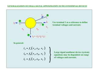
  • 1. + - VB + - VC + - VA IC IB IA ID = - ( IA + IB + IC ) 1 2 3 4 Use terminal 1 as a reference to define terminal voltages and currents In general:   C B A A A v , v , v f i    C B A B B v , v , v f i    C B A C C v , v , v f i   Large signal nonlinear device (system) equations may be dependent on range of voltages and currents. GENERALIZATION OF SMALL SIGNALAPPOXIMATION TO MULTITERMINAL DEVICES
  • 2.                                                               B A Q B A A C Q C A B Q B A A Q A A C Q C A B Q B A A Q A A C B A A A V v V v v v f V v v f V v v f V v v f V v v f V v v f V v v f V , V , V f i B A 2 C 2 2 2 B 2 2 2 A 2 2 C B A 2 1 Taylor series expansion of iA w.r.t. Q point: VA, VB, VC if |va|, |vb|, |vC| are small enough            ) t ( i c ac b ab a aa A A a v g v g v g I i     where Q A A aa aa v f r ˆ g     1 Q B A ab v i ˆ g    Q C A ac v i ˆ g   
  • 3. c ac b ab a a a v g v g v g i    c bc b b a ba b v g v g v g i    c c b cb a ca c v g v g v g i    Small signal analysis for a 4 terminal device aa g a r 1  b abv g c acv g ia1 ia2 ia3 va + - ia
  • 4. b abv g c acv g ra va + - ia vb + - ib vc + - ic c bcv g rb a bav g b cbv g rc a cav g 1 2 3 4 MOST GENERAL SMALL SIGNAL EQUIVALENT CIRCUIT FOR A 4 TERMINAL DEVICE Remarks: - All small signal parameters are Q-point dependent. - Capacitances between terminals have to be considered for high frequency analysis. - BJT and MOS are four terminal devices, only a few parameters have non negligible values. - Voltage controlled sources indicate how what happens at one port affects another port (coupling between ports).
  • 5. E B VSS C S p+ p-substrate n+ n- p n+ n+ b abv g c acv g ra va + - ia vb + - ib vc + - ic c bcv g rb a bav g b cbv g rc a cav g 1 2 3 4 c c cc s base gate emitter source collector drain substrate substrate BJT MODELLING
  • 6. c ro  v gm e b S r rb cc s c r rc c b´ v + - e´ c´ BJT MODELLING: HYBRID  MODEL Models leakage current Substrate Always connected to “signal” ground (DC voltage).            A CE 3 V V 1 T V BE V e I i i S c   C E C B i i or i i i    1   C B E i i i     Large signal equations forward active mode.
  • 7. C: Forward biased base emitter junction:   33 0 VT f e 0 1 . I where c V je e oe EB c c          C: Reversed biased base collector junction:   5 0 C 0 1 . where C oc BC V c c         CCS: Reversed biased collector substrate junction:   5 0 1 0 . where S V CS CS S oS CS c c       Large area low doping
  • 8. r: base emitter resistance:                          K . I V Q C T Q BE C Q BE B v i v i r 5 2 -1 -1    ro: output resistance:               K I V Q C A Q CE C o v i r 00 1 -1 gm: transconductance: V mA T BE C m V I Q C v i g 0 4     
  • 9. cj0, j0, , F are different for each junction, must be known. r = 5  r0  100 M can be usually neglected. re  5  strongly geometry dependent rb  200  strongly geometry dependent rc  200   Ic dependent
  • 10. EXAMPLE: Emitter area 500 m2, High voltage NPN device VEB0 = 7 V Cje0 = 1 pF joe = 0.7 V e = 0.33 VCB0 = 50 V C0 = 0.3 pF joc = 0.7 V c = 0.5 VCS0 = 70 V CCS0 = 3 pF joS = 0.52 V S = 0.5
  • 11. SMALL SIGNALANALYSIS - Set all signal sources to zero. 1.- Perform DC Analysis - Determine all DC voltages and currents if possible using DC equivalent circuits. Check for |VCE| > 0.2 V I BJT´s.  - Small signal device parameters can only be determined if DC(Q ) operating point is known. 3.- Replace devices by small - For small frequency analysis do not include parasitic signal equivalent circuits device capacitances. -Small signal equivalent circuits do not depend on the type of transistor (NPN, PNP). - Voltage sources short circuits 2.- Passivate DC Sources - Current sources open circuits  
  • 12. vS vout 15 K Q3 Q1 Q2 IBIAS1 1mA IBIAS2 5mA 3 K + 15 V - 15 V - 15 V IB1 vout 15 K 0.7 V 3 K + 15 V - 15 V - 15 V 0.7 V 0.7 V IB3 IB2  IB1  IB2  IB1  IB3 ro EXAMPLE Since We have the same VBE for Q1 and Q2: DC V V V . V V V . V V . V V m I I where m . I I I C C E C E E BIAS C BIAS C C 0 mA 5 k 3 15 .2 8 7 0 5 7 mA 0.5 k 15 - 5 1 7 0 - A 5 1 A 5 0 2 3 2 3 2 2 1 3 2 1 2 1                        
  • 13. All transistors are in active mode. V V V - V V - V EC CE CE .2 8 0 .2 8 .9 8 ) 0.7 - ( 8.2 7 15. ) 0.7 - ( 5 1 3 2 1        Calculation of small signal parameters:  = 200, VA= 100 V                    K I V r K I V r r K I V r r V I g V I g g Q C A o Q C A o o Q C T m T Q C m m T Q C m m 20 mA 5 V 100 0 0 2 mA 0.5 V 100 10 mA 0.5 mV 26 200 200 20 3 2 , 1 2 , 1 3 3 2 1 2 1 V A 3 V A 2 1    
  • 14. ro   v g i m b e b r c v + - re ro e i  e b c SIMPLIFIED SMALL SIGNAL EQUIVALENT CIRCUITS FOR BJT´S m g r    m e e e g i v r    e r (β r ) 1   
  • 15. ro3 rc3 =3 k ro1 1 1  v gm b1 r v + - e1 ro2 2 2  v gm r v + - rc2 =15 K c1 e2 c2 b2 3 3  v gm r v + - b3 c3 e3 vS rS 1 2 3 4 5 g1+ Gs - g1 - g1 g1+ g1+ go1+ g02 - g02 GC2+ go1+ g3 - g02 - g3 - g3 go3 + g3 - go3 go3 + GC3 - go3 0 0 0 0 0 0 0 0 0 0 0 0 Gs VS gm1v1+ gm2v2 - gm2v2 - gm2 v2 + gm3 v3 - gm3 v3 1 2 3 4 5 1 2 3 4 5 SISTEMATIC PROCEDURE TO WRITE NODALADMITANCE MATRIX:
  • 16. g1 + Gs - g1 - g1 g1+ g1+ go1+ g02 + gm1 + gm2 - g02 GC2+ go1+ g3 - g02 - gm2 - g3 - g3 -gm3 go3+ g3+ gm4 - go3 go3+ GC3 - go3 -gm4 0 0 0 0 0 0 0 0 0 0 0 gm3 Gs VS gm1v1+ gm2v2 - gm2v2 - gm2v2+ gm3v3 - gm3v3 1 2 3 4 5 1 2 3 4 5
  • 17. ro3 rc3 =3 k ro1 1 1  v gm b1 r v + - e1 ro2 2 2  v gm r v + - rc2 =15 K c1 e2 c2 b2 3 3  v gm r v + - b3 c3 e3 vS rS 1 2 3 4 5 c c c c c c cS3 cS2 g1+ Gs+ s c1 + s c1 - g1 - g1- s c1 g1+ g1+ go1+ g02 + gm1 + gm2 +s C2 - g02 GC2+ go1+ g3+ s CS + s c2 +s c 3 - g02 - gm2 - g3 - s c3 - g3 - gm3 - s c 3 go3+ g3+ gm4 +s c 3 - go3 go3+ GC3+ s c3 +s cS3 - go3 -gm4 0 0 0 - s c3 0 0 0 0 0 0 0 gm3 + s c3 Gs VS gm1v1+ gm2v2 - gm2v2 - gm2v2+ gm3v3 - gm3v3 1 2 3 4 5 1 2 3 4 5
  • 18. B Substrate D Drain IS ID IB IG S Source Dependent Independent B G S D i , i , i , i D S i i   0  G i Large signal equations: BS DS S G v , v , v 0  B i  Only one equation needed MOS TRANSISTOR (ENHANCEMENT)
  • 19. Saturated Mode:   1 BS DS GS D v , v , v f i  Cutoff Mode: 0  D i Nonsaturated Mode: or triode   2 BS DS GS D v , v , v f i  Weak inversion: or Subthreshold   3 BS DS GS D v , v , v f i  Strong inversion: T GS DS T GD T GS V V V V V V V      MOS TRANSISTOR: OPERATION REGIONS
  • 20. p- substrate n+ n+ p+ G S D MOS TRANSISTOR:STRUCTURE.
  • 21. MOS TRANSISTOR: LARGE SIGNAL EQUATIONS. Saturated Mode:   1 BS DS GS D v , v , v f i  kp transconductance parameter ~ T GS DS T GD T GS V V V or V V V V       - ) ( 1 1 2 2 L W T GS DS T GS p D V V v V v k i       25 A/V2 n-channel 10 A/V2 p-channel   V V 1.6 - 0.8 ~ 2 2 BS f e arg for l V V V f BS to t j j      Body effect parameter: 1 5 0  V . ~  Fermi level: V . ~ 3 0 f j Mobility degradation: m for V . ~   2 L 35 0 1   Channel length modulation: m 3 L or 3 0    f . ~
  • 22. For long dimensions ( L > 3 m ) and Low vGS ( | vGS| < 2 V       BS DS GS t GS p D v , v , v f v V v k i 1 2 DS 2        T Q GS GS V V V    is not significant no degradation     GS t GS p D v f V v k i 2 2    Used for quick hand calculations: simplified small equivalent circuits. Used to derive general small equivalent circuits Condition for small signal approximations
  • 23. cg s ro gs mv g s cg d g vg s + -  v gm vd s + - vb s + - cd b cb s d b     Q t Q GS Q D L W p Q D Q t Q GS p Q GS D m V V I I V L W k V k v i g         2 2 Output resistance: D A I V 1 -1              Q n Q DS D o I v i r  Transconductance: m L W p Q D Q BS D mb g I k v i g 2      Body effect bulk transconductance gain
  • 24. p- substrate n+ n+ p+ - - - - - B D G S VGS < Vt VDS -No current flows, electrons begin to accumulate under gate. -Strictly speaking: small current flows (subthreshold or weak inversion operation. 0 0 t GS DS V V V   
  • 25. p- substrate n+ n+ p+ B D G S VGS > Vt VDS - - - - - - - - - -Channel is induced for vGS ≥ Vt -The width of the channel is uniform, and is controlled by vGS - Vt. - For small vDS:   DS ox n DS channel L W C R 1 v V v v i t GS D    
  • 26. p- substrate n+ n+ p+ B D G S VGS > Vt VDS - - - - - - - - - - - - - - - vDS > 0 subject to: vGS > Vt , vGD > Vt vDS < vGS -Vt (small VDS!) -Nonuniform channel width, narrower in drain side than in source side: nonlinear resistive behavior.       DS t DS DS ox n - V 2 - /2 L 2 W L W C v v v v V v v i DS GS p t GS D k       Equation for triode mode
  • 27. p- substrate n+ n+ p+ B D G S VGS VDS - - - - - - - - - - - - vDS > 0 subject to: vGS > Vt , vGD < Vt vDS > vGS -Vt (large VDS!) -Channel pinch-off: channel width becomes zero on drain size. - Further increases in vDS once channel pinch-off takes place do not affect.  2 t V L 2 W   GS p D v i k
  • 28. -Large vDS , vDS > vGS -Vt Saturation mode Drain terminal performs as high impedance source depending only on vDS -Smal vDS , vDS < vGS -Vt Triode mode Device acts as a voltage controlled resistor - Equations are valid for long channel devices !!!!! REMARKS.
  • 29. The behavior of short-channel transistors (sub-micron channel length) deviate from that of the long-channel transistors. A MOS transistor is called short channel device if its channel length is of the same order of magnitude as the depletion region thickness of the source and drain junctions. Alternatively, a MOSFET transistor can be defined as a short-channel device if the effective length   d D eff x L L    2 is approximately equal to the source and drain junction depth j x MOSFETs – Short channel effects tox n+ n+ Cross section L Gate oxide xj
  • 30. The short channel effects that arises in this case are attributed to two physical phenomena: (i) The limitation imposed on electron drift characteristics in the channel, and (ii) the modification of the threshold voltage due to shortening channel length. MOSFETs – Short channel effects
  • 31. MOSFETs – Short channel effects Fundamental scaling limits for conventional MOS devices
  • 32. MOSFETs – Short channel effects – Mobility Degradation • Transistors with channel lengths < 1um • High gate voltage • Large electric fields, no longer one-dimensional • Greater channel depth • More electron collisions • Carrier mobility n degraded • Carrier velocity between source & drain saturates • Channel’s effective sheet resistance goes up • How can we model mobility degradation? • Use finite series source resistance Rsx: • Rsx = (1/Ec) (1/ nCox) (1/W) • where Ec = critical electric field ~ 1.5X1E6 v/m
  • 33. MOSFETs – Short channel effects – Mobility Degradation For 0.8m long transistor with nCox = 90 /V2, Rsx = 6K/m width - much larger than physical source resistance Id/Vgs square law no longer true - relationship somewhere between linear and square law
  • 34. MOSFETs – Short channel effects Threshold Variations VT L Long-channel threshold LowVDS threshold Threshold as a function of the length (for low VDS) Drain-induced barrier lowering (for lowL) VDS VT
  • 35. MOSFETs – Short channel effects Velocity Saturation – In long channel devices, the drift velocity of the carriers, vd, is proportional to the electric field, independent of the value of the field, Ex. Note that the lateral (horizontal) electric field, along the channel increases, as the effective channel length decreases. – For channel electric field of Ex ≥ 105 V/cm, the electron drift velocity in the channel reaches a saturation value of vd = 105 V/sec. In this case, the carriers fail to follow the linear model. The critical value of the electric field at which the carrier velocity saturates, EC, depends on the doping levels and the vertical electrical field applied (The vertical electric field is due the voltage applied on the gate of the MOSFET). eff DS d L v v     E vd    c d E E E v / 1     
  • 36. MOSFETs – Short channel effects Velocity Saturation The velocity saturation has very significant implications upon the current-voltage characteristics of the short-channel MOSFET, especially the n-type MOSFET. For short-channel, these implications include: 1. Due to carrier velocity saturation, the delivered saturation-mode current is less than the current value predicted by the conventional long-channel current equation. The current is no longer a quadratic function of the gate-to-source voltage,, and it is virtually independent of the channel length. The saturation current displays a linear dependence with respect to. 2. The device enters saturation before reaches, i.e., . 3. The actual threshold voltage of the short-channel devices is less than that of the long-channel devices. 4. In the surface region of the channel, i.e., the region under the gate oxide, the surface mobility of the carriers is reduced with respect to the bulk mobility.
  • 37. MOSFETs – Short channel effects Velocity Saturation x (V/µm) x c = 1.5 u n (m/s) usat = 10 5 Constant mobility (slope = µ) Constant velocity
  • 38. MOSFETs – Short channel effects Linear Relationship -4 VDS(V) 0 0.5 1 1.5 2 2.5 0 0.5 1 1.5 2 2.5 x 10 I D (A) VGS= 2.5 V VGS= 2.0 V VGS= 1.5 V VGS= 1.0 V Early Saturation
  • 39. MOSFETs – Short channel effects ID Long-channel device Short-channel device VDS VDSAT VGS - V T VGS= V DD
  • 40. ID versus VGS 0 0.5 1 1.5 2 2.5 0 1 2 3 4 5 6 x 10 -4 V GS(V) I D (A) 0 0.5 1 1.5 2 2.5 0 0.5 1 1.5 2 2.5 x 10 -4 V GS(V) I D (A) quadratic quadratic linear Long Channel Short Channel
  • 41. ID versus VDS -4 V DS(V) 0 0.5 1 1.5 2 2.5 0 0.5 1 1.5 2 2.5 x 10 I D (A) VGS= 2.5 V VGS= 2.0 V VGS= 1.5 V VGS= 1.0 V 0 0.5 1 1.5 2 2.5 0 1 2 3 4 5 6 x 10 -4 VDS(V) I D (A) VGS= 2.5 V VGS= 2.0 V VGS= 1.5 V VGS= 1.0 V Resistive Saturation VDS = VGS - VT Long Channel Short Channel
  • 42. Hot Carrier Effects • Hot Carrier effects - term used to describe mobility reduction and velocity saturation (as temp increases, electron mobility decreases) • Hot Carriers can tunnel through gate oxide and cause finite gate currents • Can become trapped in gate oxide causing threshold voltage to gradually change • Can cause impact ionization - avalanche breakdown • Finite Drain to Ground impedance - current flows from drain to bulk • Latch-up may occur due to substrate currents • Lowered Output resistance • Source-drain “punch-through” - high energy electrons shoot from S to D via abnormal conduction mechanism not governed by drift equations; unlimited current flow, transistor may breakdown MOSFETs – Short channel effects
  • 43. MOSFETs – Short channel effects Reduced Output Impedance • Widening depletion region at drain end affects drain current more for short channel devices • Id - Vds characteristic not as flat: output impedance reduced • Phenomenon also known as “dibble” - DIBL or drain induced barrier lowering: effective lowering of threshold voltage as Vds is increased giving greater Id and less output impedance as channel shortened • Can be a problem! Use cascode configuration • Which are more prone to hot carrier effects: N or P channel MOSFETs ?
  • 44. • Sub Threshold Operation/Region – weak inversion - sub threshold region – Cdep also depends on interface state density ) / ( nkT qV DO d GS e L W I I  ox dep ox C C C n   MOSFETs – Short channel effects 0 0.5 1 1.5 2 2.5 10 -12 10 -10 10 -8 10 -6 10 -4 10 -2 V GS(V) I D (A) VT Linear Exponential Quadratic Typical values for S: 60 .. 100 mV/decade S is DVGS for ID2/ID1 =10
  • 45. d o i j o x n qA I  2  MOSFETs – Short channel effects Sub-Threshold ID vs VDS   DS kT qV nkT qV D V e e I I DS GS               1 1 0 VGS from 0 to 0.3V
  • 46. MOSFETs – Short channel effects Sub-Threshold ID vs VGS VDS from 0 to 0.5V            kT qV nkT qV D DS GS e e I I 1 0
  • 47. Leakage Currents d o i j o x n qA I  2  MOSFETs – Short channel effects •Currents at reverse biased pn junctions •Result in static dissipation •Determine max hold time for sample and hold circuit or dynamic memory cell •Strong function of temperature - doubles for every 11 deg C rise of temp
  • 48. • SPICE Model Parameters MOSFETs – Short channel effects
  • 49. • Short Channel Effects - what happens as L is decreased …. – Increased Channel Length Modulation – DIBL (drain induced barrier lowering) MOSFETs – Short channel effects
  • 50. Future Perspectives 25 nm FINFET MOS transistor
  • 51.
  • 52. MOSFETs – Short channel effects • Short Channel Effects - what happens as L is decreased …. – Mobility Degradation – Velocity Saturation E vd    c d E E E v / 1     
  • 53. MOSFETs – Short channel effects • Short Channel Effects - what happens as L is decreased …. – Mobility Degradation – Velocity Saturation E vd    c d E E E v / 1     