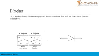
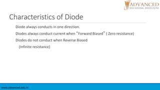
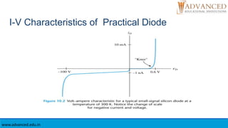
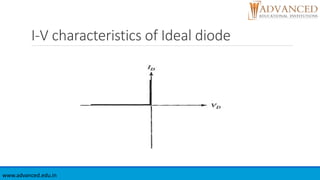
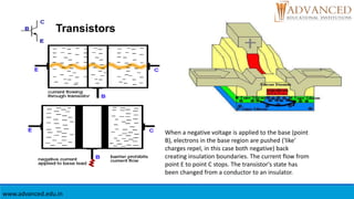
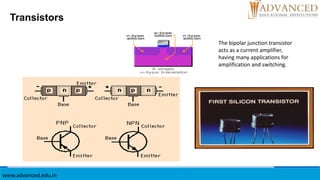
Semiconductor Device
BY
ABHA AGRAWAL
DESIGNATION – ASTT. PROFFESSOR
www.advanced.edu.in
Overview
Introduction
What are P-type and N-type semiconductors??
What are Diodes?
Characteristics Of Diode
I – V Characteristics of Diodes
Diode as Rectifiers
Forward Bias & Reverse Bias
Shockley Equation
Transistors
Transistors as Amplifiers
www.advanced.edu.in
Introduction
www.advanced.edu.in
Semiconductor device, electronic circuit component made from a material that
is neither a good conductor nor a good insulator (hence semiconductor).
Such devices have found wide applications because of their compactness,
reliability, and low cost. As discrete components, they have found use in power
devices, optical sensors, and light emitters including solid-state lasers.
www.advanced.edu.in
Examples of Semiconductor Device
What are P-type and N-type ?
Semiconductors are classified in to P-type and N-type semiconductor
P-type: A P-type material is one in which holes are majority carriers i.e. they
are positively charged materials (++++)
N-type: A N-type material is one in which electrons are majority charge carriers
i.e. they are negatively charged materials (-----)
www.advanced.edu.in
Diodes
It is represented by the following symbol, where the arrow indicates the direction of positive
current flow.
www.advanced.edu.in
Characteristics of Diode
Diode always conducts in one direction.
Diodes always conduct current when “Forward Biased” ( Zero resistance)
Diodes do not conduct when Reverse Biased
(Infinite resistance)
www.advanced.edu.in
I-V Characteristics of Practical Diode
www.advanced.edu.in
I-V characteristics of Ideal diode
www.advanced.edu.in
Forward Bias and Reverse Bias
Forward Bias : Connect positive of the Diode to positive of supply…negative of Diode to negative
of supply
Reverse Bias: Connect positive of the Diode to negative of supply…negative of diode to positive
of supply.
www.advanced.edu.in
Shockley Equation












 1exp
T
D
sD
nV
v
Ii
q
kT
VT 
Is is the saturation current ~10 -14
Vd is the diode voltage
n – emission coefficient (varies from 1 - 2 )
k = 1.38 × 10⁻²³ J/K is Boltzmann’s constant
q = 1.60 × 10⁻¹⁹ C is the electrical charge of an electron.
At a temperature of 300 K, we have
mV26TV
www.advanced.edu.in
Rectification
Converting ac to dc is accomplished by the process of rectification.
Two processes are used:
◦ Half-wave rectification;
◦ Full-wave rectification.
www.advanced.edu.in
Transistors
When a negative voltage is applied to the base (point
B), electrons in the base region are pushed ('like'
charges repel, in this case both negative) back
creating insulation boundaries. The current flow from
point E to point C stops. The transistor's state has
been changed from a conductor to an insulator.
www.advanced.edu.in
Transistors
The bipolar junction transistor
acts as a current amplifier,
having many applications for
amplification and switching.
www.advanced.edu.in
Transistors
www.advanced.edu.in
Unbiased Transistors
www.advanced.edu.in
Transistors: Amplifier
Apply different values of the
base bias voltage and the
collector bias voltage to the
npn transistor and see
what happens.
With two ammeters (shown as red dots) and a voltmeter to measure VCE we can
determine the characteristics of the transistor.
www.advanced.edu.in
Transistors: Amplifier
The amount of base current is
determined by the base bias
voltage.
B
C
I
I

www.advanced.edu.in
Conclusion
www.advanced.edu.in
Semiconductor devices have a wide range of current- and voltage-handling
capabilities, with current ratings from a few Nanoamperes (10−9 ampere) to more
than 5,000 amperes and voltage ratings extending above 100,000 volts.
lSemiconductor devices lend themselves to integration into complex but readily
manufacturable microelectronic circuits. They are, and will be in the foreseeable
future, the key elements for the majority of electronic systems, including
communications, consumer, data-processing, and industrial-control equipment.
Contact Information
Abha Agrawal
Designation – Astt. Proffessor
Email-Id – abha8024@gmail.com
Advanced Educational Institutions
70 km. Delhi-Mathura Road,
Aurangabad, Distt. Palwal
Haryana, India
01275-302214, 9354260374
www.advanced.edu.in

Semiconductor devices

  • 1.
    Semiconductor Device BY ABHA AGRAWAL DESIGNATION– ASTT. PROFFESSOR www.advanced.edu.in
  • 2.
    Overview Introduction What are P-typeand N-type semiconductors?? What are Diodes? Characteristics Of Diode I – V Characteristics of Diodes Diode as Rectifiers Forward Bias & Reverse Bias Shockley Equation Transistors Transistors as Amplifiers www.advanced.edu.in
  • 3.
    Introduction www.advanced.edu.in Semiconductor device, electroniccircuit component made from a material that is neither a good conductor nor a good insulator (hence semiconductor). Such devices have found wide applications because of their compactness, reliability, and low cost. As discrete components, they have found use in power devices, optical sensors, and light emitters including solid-state lasers.
  • 4.
  • 5.
    What are P-typeand N-type ? Semiconductors are classified in to P-type and N-type semiconductor P-type: A P-type material is one in which holes are majority carriers i.e. they are positively charged materials (++++) N-type: A N-type material is one in which electrons are majority charge carriers i.e. they are negatively charged materials (-----) www.advanced.edu.in
  • 6.
    Diodes It is representedby the following symbol, where the arrow indicates the direction of positive current flow. www.advanced.edu.in
  • 7.
    Characteristics of Diode Diodealways conducts in one direction. Diodes always conduct current when “Forward Biased” ( Zero resistance) Diodes do not conduct when Reverse Biased (Infinite resistance) www.advanced.edu.in
  • 8.
    I-V Characteristics ofPractical Diode www.advanced.edu.in
  • 9.
    I-V characteristics ofIdeal diode www.advanced.edu.in
  • 10.
    Forward Bias andReverse Bias Forward Bias : Connect positive of the Diode to positive of supply…negative of Diode to negative of supply Reverse Bias: Connect positive of the Diode to negative of supply…negative of diode to positive of supply. www.advanced.edu.in
  • 11.
    Shockley Equation              1exp T D sD nV v Ii q kT VT Is is the saturation current ~10 -14 Vd is the diode voltage n – emission coefficient (varies from 1 - 2 ) k = 1.38 × 10⁻²³ J/K is Boltzmann’s constant q = 1.60 × 10⁻¹⁹ C is the electrical charge of an electron. At a temperature of 300 K, we have mV26TV www.advanced.edu.in
  • 12.
    Rectification Converting ac todc is accomplished by the process of rectification. Two processes are used: ◦ Half-wave rectification; ◦ Full-wave rectification. www.advanced.edu.in
  • 13.
    Transistors When a negativevoltage is applied to the base (point B), electrons in the base region are pushed ('like' charges repel, in this case both negative) back creating insulation boundaries. The current flow from point E to point C stops. The transistor's state has been changed from a conductor to an insulator. www.advanced.edu.in
  • 14.
    Transistors The bipolar junctiontransistor acts as a current amplifier, having many applications for amplification and switching. www.advanced.edu.in
  • 15.
  • 16.
  • 17.
    Transistors: Amplifier Apply differentvalues of the base bias voltage and the collector bias voltage to the npn transistor and see what happens. With two ammeters (shown as red dots) and a voltmeter to measure VCE we can determine the characteristics of the transistor. www.advanced.edu.in
  • 18.
    Transistors: Amplifier The amountof base current is determined by the base bias voltage. B C I I  www.advanced.edu.in
  • 19.
    Conclusion www.advanced.edu.in Semiconductor devices havea wide range of current- and voltage-handling capabilities, with current ratings from a few Nanoamperes (10−9 ampere) to more than 5,000 amperes and voltage ratings extending above 100,000 volts. lSemiconductor devices lend themselves to integration into complex but readily manufacturable microelectronic circuits. They are, and will be in the foreseeable future, the key elements for the majority of electronic systems, including communications, consumer, data-processing, and industrial-control equipment.
  • 20.
    Contact Information Abha Agrawal Designation– Astt. Proffessor Email-Id – abha8024@gmail.com Advanced Educational Institutions 70 km. Delhi-Mathura Road, Aurangabad, Distt. Palwal Haryana, India 01275-302214, 9354260374 www.advanced.edu.in