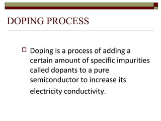
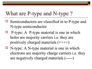
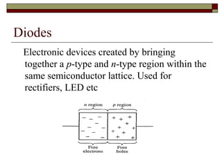
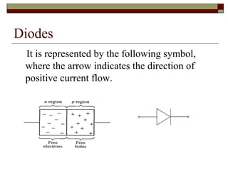
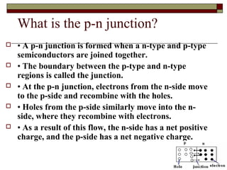
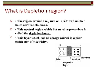
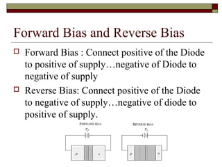
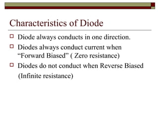
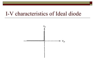
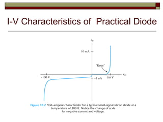
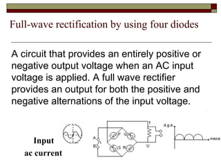
SEMICONDUCTORS
Overview
 Semiconductors
 What are P-type and N-type semiconductors??
 What are Diodes?
 Forward Bias & Reverse Bias
 Characteristics Of Ideal Diode
 I – V Characteristics of Diodes
 Rectification
Introduction
Semiconductors are materials
whose electrical properties lie
between Conductors and
Insulators.
Ex : Silicon and Germanium
Intrinsic & Extrinsic Semiconductor
 Semiconductors that are free of doping impurities
are called intrinsic semiconductors.
 Semiconductors formed after adding impurities are
called extrinsic semiconductors.
 Doping is a process of adding a
certain amount of specific impurities
called dopants to a pure
semiconductor to increase its
electricity conductivity.
DOPING PROCESS
What are P-type and N-type ?
 Semiconductors are classified in to P-type and
N-type semiconductor
 P-type: A P-type material is one in which
holes are majority carriers i.e. they are
positively charged materials (++++)
 N-type: A N-type material is one in which
electrons are majority charge carriers i.e. they
are negatively charged materials (-----)
Diodes
Electronic devices created by bringing
together a p-type and n-type region within the
same semiconductor lattice. Used for
rectifiers, LED etc
Diodes
It is represented by the following symbol,
where the arrow indicates the direction of
positive current flow.
What is the p-n junction?
 • A p-n junction is formed when a n-type and p-type
semiconductors are joined together.
 • The boundary between the p-type and n-type
regions is called the junction.
 • At the p-n junction, electrons from the n-side move
to the p-side and recombine with the holes.
 • Holes from the p-side similarly move into the n-
side, where they recombine with electrons.
 • As a result of this flow, the n-side has a net positive
charge, and the p-side has a net negative charge.
 • The region around the junction is left with neither
holes nor free electrons.
 • This neutral region which has no charge carriers is
called the depletion layer.
 • This layer which has no charge carrier is a poor
conductor of electricity.
What is Depletion region?
Forward Bias and Reverse Bias
 Forward Bias : Connect positive of the Diode
to positive of supply…negative of Diode to
negative of supply
 Reverse Bias: Connect positive of the Diode
to negative of supply…negative of diode to
positive of supply.
Characteristics of Diode
 Diode always conducts in one direction.
 Diodes always conduct current when
“Forward Biased” ( Zero resistance)
 Diodes do not conduct when Reverse Biased
(Infinite resistance)
I-V characteristics of Ideal diode
I-V Characteristics of Practical Diode
Rectification
 Converting ac to dc is accomplished by the
process of rectification.
 Two processes are used:
 Half-wave rectification;
 Full-wave rectification.
Half-wave Rectification
 Simplest process used
to convert ac to dc.
 A diode is used to clip
the input signal
excursions of one
polarity to zero.
Full-wave rectification by using four diodes
Input
ac current
A circuit that provides an entirely positive or
negative output voltage when an AC input
voltage is applied. A full wave rectifier
provides an output for both the positive and
negative alternations of the input voltage.
Semi conductor

Semi conductor

  • 1.
  • 2.
    Overview  Semiconductors  Whatare P-type and N-type semiconductors??  What are Diodes?  Forward Bias & Reverse Bias  Characteristics Of Ideal Diode  I – V Characteristics of Diodes  Rectification
  • 3.
    Introduction Semiconductors are materials whoseelectrical properties lie between Conductors and Insulators. Ex : Silicon and Germanium
  • 4.
    Intrinsic & ExtrinsicSemiconductor  Semiconductors that are free of doping impurities are called intrinsic semiconductors.  Semiconductors formed after adding impurities are called extrinsic semiconductors.
  • 5.
     Doping isa process of adding a certain amount of specific impurities called dopants to a pure semiconductor to increase its electricity conductivity. DOPING PROCESS
  • 6.
    What are P-typeand N-type ?  Semiconductors are classified in to P-type and N-type semiconductor  P-type: A P-type material is one in which holes are majority carriers i.e. they are positively charged materials (++++)  N-type: A N-type material is one in which electrons are majority charge carriers i.e. they are negatively charged materials (-----)
  • 7.
    Diodes Electronic devices createdby bringing together a p-type and n-type region within the same semiconductor lattice. Used for rectifiers, LED etc
  • 8.
    Diodes It is representedby the following symbol, where the arrow indicates the direction of positive current flow.
  • 9.
    What is thep-n junction?  • A p-n junction is formed when a n-type and p-type semiconductors are joined together.  • The boundary between the p-type and n-type regions is called the junction.  • At the p-n junction, electrons from the n-side move to the p-side and recombine with the holes.  • Holes from the p-side similarly move into the n- side, where they recombine with electrons.  • As a result of this flow, the n-side has a net positive charge, and the p-side has a net negative charge.
  • 10.
     • Theregion around the junction is left with neither holes nor free electrons.  • This neutral region which has no charge carriers is called the depletion layer.  • This layer which has no charge carrier is a poor conductor of electricity. What is Depletion region?
  • 11.
    Forward Bias andReverse Bias  Forward Bias : Connect positive of the Diode to positive of supply…negative of Diode to negative of supply  Reverse Bias: Connect positive of the Diode to negative of supply…negative of diode to positive of supply.
  • 12.
    Characteristics of Diode Diode always conducts in one direction.  Diodes always conduct current when “Forward Biased” ( Zero resistance)  Diodes do not conduct when Reverse Biased (Infinite resistance)
  • 13.
  • 14.
    I-V Characteristics ofPractical Diode
  • 15.
    Rectification  Converting acto dc is accomplished by the process of rectification.  Two processes are used:  Half-wave rectification;  Full-wave rectification.
  • 16.
    Half-wave Rectification  Simplestprocess used to convert ac to dc.  A diode is used to clip the input signal excursions of one polarity to zero.
  • 17.
    Full-wave rectification byusing four diodes Input ac current A circuit that provides an entirely positive or negative output voltage when an AC input voltage is applied. A full wave rectifier provides an output for both the positive and negative alternations of the input voltage.