SPICE MODEL of TPCP8102 (Standard+BDS Model) in SPICE PARK
•
0 likes•282 views

SPICE MODEL of TPCP8102 (Standard+BDS) in SPICE PARK. English Version is http://www.spicepark.net. Japanese Version is http://www.spicepark.com by Bee Technologies.

Recommended
Recommended
More Related Content
What's hot
What's hot (20)
Viewers also liked
Viewers also liked (11)
Similar to SPICE MODEL of TPCP8102 (Standard+BDS Model) in SPICE PARK
Similar to SPICE MODEL of TPCP8102 (Standard+BDS Model) in SPICE PARK (20)
More from Tsuyoshi Horigome
More from Tsuyoshi Horigome (20)
Recently uploaded
Recently uploaded (20)
SPICE MODEL of TPCP8102 (Standard+BDS Model) in SPICE PARK
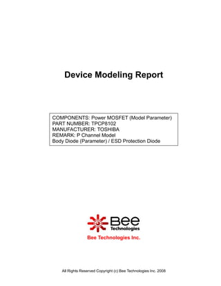
- 1. Device Modeling Report COMPONENTS: Power MOSFET (Model Parameter) PART NUMBER: TPCP8102 MANUFACTURER: TOSHIBA REMARK: P Channel Model Body Diode (Parameter) / ESD Protection Diode Bee Technologies Inc. All Rights Reserved Copyright (c) Bee Technologies Inc. 2008
- 2. MOSFET MODEL Pspice model Model description parameter LEVEL L Channel Length W Channel Width KP Transconductance RS Source Ohmic Resistance RD Ohmic Drain Resistance VTO Zero-bias Threshold Voltage RDS Drain-Source Shunt Resistance TOX Gate Oxide Thickness CGSO Zero-bias Gate-Source Capacitance CGDO Zero-bias Gate-Drain Capacitance CBD Zero-bias Bulk-Drain Junction Capacitance MJ Bulk Junction Grading Coefficient PB Bulk Junction Potential FC Bulk Junction Forward-bias Capacitance Coefficient RG Gate Ohmic Resistance IS Bulk Junction Saturation Current N Bulk Junction Emission Coefficient RB Bulk Series Resistance PHI Surface Inversion Potential GAMMA Body-effect Parameter DELTA Width effect on Threshold Voltage ETA Static Feedback on Threshold Voltage THETA Modility Modulation KAPPA Saturation Field Factor VMAX Maximum Drift Velocity of Carriers XJ Metallurgical Junction Depth UO Surface Mobility All Rights Reserved Copyright (c) Bee Technologies Inc. 2008
- 3. Transconductance Characteristic Circuit Simulation Result 25 20 15 gfs 10 5 Measurement Simulation 0 0 1 2 3 4 5 - ID - Drain Current - A Comparison table gfs -Id(A) Error(%) Measurement Simulation 0.2 2.500 2.557 2.280 0.5 6.250 6.400 2.400 1 10.000 10.000 0.000 2 14.286 15.000 4.998 5 20.833 21.714 4.229 All Rights Reserved Copyright (c) Bee Technologies Inc. 2008
- 4. Vgs-Id Characteristic Circuit Simulation result -12A -10A -8A -6A -4A -2A 0A 0V -1.0V -2.0V -3.0V I(V3) V_V1 Evaluation circuit V3 0Vdc U1 TPCP8102 V2 -10 V1 -3 0 All Rights Reserved Copyright (c) Bee Technologies Inc. 2008
- 5. Comparison Graph Circuit Simulation Result 12 Measurement Simulation 10 8 - ID - Drain Current - A 6 4 2 0 0 1 2 3 - VGS - Gate to Source Voltage - V Simulation Result -VGS(V) -ID(A) Error (%) Measurement Simulation 0.1 1.185 1.163 -1.857 0.5 1.270 1.216 -4.252 1 1.320 1.256 -4.848 2 1.385 1.318 -4.838 5 1.525 1.450 -4.918 10 1.700 1.616 -4.941 12 1.760 1.674 -4.886 All Rights Reserved Copyright (c) Bee Technologies Inc. 2008
- 6. Rds(on) Characteristic Circuit Simulation result -5.0A -4.0A -3.0A -2.0A -1.0A 0A 0V -20mV -40mV -60mV -80mV I(V2) V_V3 Evaluation circuit V2 0Vdc U1 TPCP8102 V3 0Vdc V1 -10 0 Simulation Result ID=-3.6A, VGS=-4.5V Measurement Simulation Error (%) R DS (on) 13.500 m 13.495 m -0.037 All Rights Reserved Copyright (c) Bee Technologies Inc. 2008
- 7. Gate Charge Characteristic Circuit Simulation result -8.0V -6.0V -4.0V -2.0V 0V 0 10n 20n 30n 40n V(W1:4) Time*1mA Evaluation circuit U1 TPCP8102 W - + I2 D1 W1 Dbreak -7.2 IOFF = 1mA I1 TD = 0 ION = 0 TF = 1n ROFF = 1e6 PW = 600u RON = 1.0 V1 PER = 1500u I1 = 0 I2 = 1m -16 TR = 1n 0 Simulation Result VDD=-16V,ID=-7.2A Measurement Simulation Error (%) ,VGS=-5V Qgs 5.400 nC 5.415 nC 0.278 Qgd 10.000 nC 10.018 nC 0.180 Qg 33.000 nC 27.823 nC -15.688 All Rights Reserved Copyright (c) Bee Technologies Inc. 2008
- 8. Capacitance Characteristic Measurement Simulation Simulation Result Cbd(pF) VDS(V) Error(%) Measurement Simulation 0.1 250.000 249.500 -0.200 0.2 225.000 224.000 -0.444 0.5 180.000 181.000 0.556 1 142.000 142.000 0.000 2 106.000 106.000 0.000 5 68.000 68.050 0.074 10 48.000 48.000 0.000 20 35.000 34.990 -0.029 All Rights Reserved Copyright (c) Bee Technologies Inc. 2008
- 9. Switching Time Characteristic Circuit Simulation result -6.0V -5.0V -4.0V -3.0V -2.0V -1.0V 0V 1.94us 1.98us 2.02us 2.06us 2.10us 2.14us 2.18us 2.22us V(U1:4) V(U1:5)/2 Time Evaluation circuit L1 R3 30nH 2.77 U1 TPCP8102 R1 L2 -10 V1 30nH 4.7 V1 = 0 V2 V2 = -10 R2 TD = 2u TR = 10n 4.7 TF = 10n PW = 10u PER = 50u 0 Simulation Result ID=-3.6A, VDD=-10V Measurement Simulation Error(%) VGS=-5V ton 14.000 ns 14.060 ns 0.429 All Rights Reserved Copyright (c) Bee Technologies Inc. 2008
- 10. Output Characteristic Circuit Simulation result -10A -1.8 -1.7V -10 -1.9 -2 -8A -3 -5 -6A -1.6V -4A -1.5V -2A -1.4V VGS= -1.3V 0A 0V -0.4V -0.8V -1.2V -1.6V -2.0V I(V3) V_V2 Evaluation circuit V3 0Vdc U1 TPCP8102 V2 -2V V1 0 0 All Rights Reserved Copyright (c) Bee Technologies Inc. 2008
- 11. BODY DIODE SPICE MODEL Forward Current Characteristic Circuit Simulation Result -100A 3 -100mA 0V 0.2V 0.4V 0.6V 0.8V 1.0V 1.2V -I(R1) V_V1 Evaluation Circuit R1 0.01m V1 0Vdc U1 TPCP8102 0 All Rights Reserved Copyright (c) Bee Technologies Inc. 2008
- 12. Comparison Graph Circuit Simulation Result 100 Measurement Simulation - Drain reverse current IDR(A) 10 1 0.1 0 0.2 0.4 0.6 0.8 1 1.2 - Drain Source voltage VDS(V) Simulation Result -VDS(V) -VDS(V) -IDR(A) %Error Measurement Simulation 0.100 0.535 0.534 -0.187 0.200 0.560 0.560 0.000 0.500 0.600 0.600 0.000 1.000 0.640 0.639 -0.156 2.000 0.690 0.691 0.145 5.000 0.790 0.788 -0.253 10.000 0.900 0.900 0.000 All Rights Reserved Copyright (c) Bee Technologies Inc. 2008
- 13. Reverse Recovery Characteristic Circuit Simulation Result 400mA 200mA 0A -200mA -400mA 19.88us 19.96us 20.04us 20.12us 20.20us 20.28us I(RL) Time Evaluation Circuit RL 50 V1 = -9.59 V1 U1 V2 = 10.5 TPCP8102 TD = 29n TR = 10n TF = 10n PW = 20u PER = 100u 0 Compare Measurement vs. Simulation Measurement Simulation Error (%) trj 17.600 ns 17.657 ns 0.324 All Rights Reserved Copyright (c) Bee Technologies Inc. 2008
- 14. Reverse Recovery Characteristic Reference Trj=17.6(ns) Trb=60.8(ns) Conditions:Ifwd=lrev=0.2(A),Rl=50 p Example Relation between trj and trb All Rights Reserved Copyright (c) Bee Technologies Inc. 2008
- 15. ESD PROTECTION DIODE SPICE MODEL Zener Voltage Characteristic Circuit Simulation Result 10mA 5mA 0A 0V 5V 10V 15V 20V 25V 30V 35V 40V 45V 50V I(R1) V_V1 Evaluation Circuit U1 TPCP8102 R2 R1 1G 0.01m V1 0Vdc 0 All Rights Reserved Copyright (c) Bee Technologies Inc. 2008
- 16. Zener Voltage Characteristic Reference All Rights Reserved Copyright (c) Bee Technologies Inc. 2008