SPICE MODEL of 2SJ567 (Standard+BDS Model) in SPICE PARK
•
0 likes•268 views

SPICE MODEL of 2SJ567 (Standard+BDS) in SPICE PARK. English Version is http://www.spicepark.net. Japanese Version is http://www.spicepark.com by Bee Technologies.

Recommended
Recommended
More Related Content
What's hot
What's hot (20)
Similar to SPICE MODEL of 2SJ567 (Standard+BDS Model) in SPICE PARK
Similar to SPICE MODEL of 2SJ567 (Standard+BDS Model) in SPICE PARK (20)
More from Tsuyoshi Horigome
More from Tsuyoshi Horigome (20)
Recently uploaded
Recently uploaded (20)
SPICE MODEL of 2SJ567 (Standard+BDS Model) in SPICE PARK
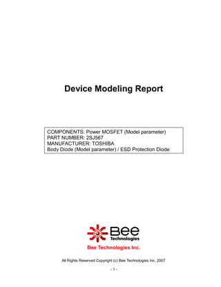
- 1. Device Modeling Report COMPONENTS: Power MOSFET (Model parameter) PART NUMBER: 2SJ567 MANUFACTURER: TOSHIBA Body Diode (Model parameter) / ESD Protection Diode Bee Technologies Inc. All Rights Reserved Copyright (c) Bee Technologies Inc. 2007 -1-
- 2. SPICE MODEL P-Channel 2 1 3 All Rights Reserved Copyright (c) Bee Technologies Inc. 2007 -2-
- 3. MOSFET MODEL PSpice model Model description parameter LEVEL L Channel Length W Channel Width KP Transconductance RS Source Ohmic Resistance RD Ohmic Drain Resistance VTO Zero-bias Threshold Voltage RDS Drain-Source Shunt Resistance TOX Gate Oxide Thickness CGSO Zero-bias Gate-Source Capacitance CGDO Zero-bias Gate-Drain Capacitance CBD Zero-bias Bulk-Drain Junction Capacitance MJ Bulk Junction Grading Coefficient PB Bulk Junction Potential FC Bulk Junction Forward-bias Capacitance Coefficient RG Gate Ohmic Resistance IS Bulk Junction Saturation Current N Bulk Junction Emission Coefficient RB Bulk Series Resistance PHI Surface Inversion Potential GAMMA Body-effect Parameter DELTA Width effect on Threshold Voltage ETA Static Feedback on Threshold Voltage THETA Mobility Modulation KAPPA Saturation Field Factor VMAX Maximum Drift Velocity of Carriers XJ Metallurgical Junction Depth UO Surface Mobility All Rights Reserved Copyright (c) Bee Technologies Inc. 2007 -3-
- 4. Transconductance Characteristic Circuit Simulation Result 10 Measurement Simulation TRANSCONDUCTANCE GFS(s) 1 0.1 0 0.5 1 1.5 2 DRIAN CURRENT ID (A) Comparison table gfs - Id(A) Error(%) Measurement Simulation 0.1 0.4400 0.4505 2.3751 0.2 0.6060 0.6349 4.7724 0.5 1.0310 1.0000 -3.0068 1 1.4290 1.4104 -1.2990 2 2.0000 1.9802 -0.9901 All Rights Reserved Copyright (c) Bee Technologies Inc. 2007 -4-
- 5. Vgs-Id Characteristic Circuit Simulation result -2.0A -1.8A -1.6A -1.4A -1.2A -1.0A -0.8A -0.6A -0.4A -0.2A 0A 0V -2V -4V -6V -8V -10V I(Vsense) V_VGS Evaluation circuit Vsense U2 2SJ567_P VDS -10Vdc VGS 0 All Rights Reserved Copyright (c) Bee Technologies Inc. 2007 -5-
- 6. Comparison Graph Circuit Simulation Result 5 Measurement Simulation 4 - Drain Current ID (A) 3 2 1 0 0 2 4 6 8 10 - Gate - Source Voltage VGS (V) Simulation Result - VGS(V) - ID(A) Error (%) Measurement Simulation 0.1 3.450 3.473 0.661 0.2 3.643 3.662 0.508 0.5 4.000 4.037 0.925 1 4.480 4.462 -0.406 2 5.067 5.065 -0.036 3 5.500 5.531 0.562 4 5.900 5.925 0.424 All Rights Reserved Copyright (c) Bee Technologies Inc. 2007 -6-
- 7. Rds(on) Characteristic Circuit Simulation result -1.50A -1.38A -1.25A -1.13A -1.00A -0.88A -0.75A -0.63A -0.50A -0.38A -0.25A -0.13A 0A 0V -0.6V -1.2V -1.8V -2.4V -3.0V -3.6V -4.2V I(Vsense) V_VDS Evaluation circuit Vsense U1 2SJ567 VDS VGS -10Vdc 0 Simulation Result ID=-1.5A, VGS=-10V Measurement Simulation Error (%) R DS (on) 1.600 1.600 0.000 All Rights Reserved Copyright (c) Bee Technologies Inc. 2007 -7-
- 8. Gate Charge Characteristic Circuit Simulation result -16V -12V -8V -4V 0V 0 4n 8n 12n 16n 20n V(W1:1) Time*1mA Evaluation circuit Vsense I1 Dbreak D1 -2.5Adc W 2SJ567_P - TD = 0 + I2 W1 VD ION = 0A -160Vdc IOFF = 1mA 0 Simulation Result VDD=-160V,ID=-2.5A Measurement Simulation Error (%) Qgs 2.000 nC 2.0098 nC 0.490 Qgd 4.000 nC 3.973 nC -0.675 Qg 10.000 nC 7.6815 nC -23.185 All Rights Reserved Copyright (c) Bee Technologies Inc. 2007 -8-
- 9. Capacitance Characteristic Simulation Result Cbd(pF) - VDS(V) Error(%) Measurement Simulation 0.1 460.000 459.000 -0.217 0.2 400.000 400.000 0.000 0.5 310.000 308.000 -0.645 1 240.000 241.000 0.417 2 180.000 181.000 0.556 5 115.000 114.000 -0.870 10 80.000 79.500 -0.625 20 57.000 56.880 -0.211 30 47.000 46.550 -0.957 All Rights Reserved Copyright (c) Bee Technologies Inc. 2007 -9-
- 10. Switching Time Characteristic Circuit Simulation result -14V -12V ___ VOUT/10 ___ VGS -10V -8V -6V -4V -2V 0V 2V 0.8us 0.9us 1.0us 1.1us 1.2us 1.3us V(L3:1) V(L2:2)/10 Time Evaluation circuit RL 3 66.7 R1 L3 2 30nH V1 = 0 50 VD V2 = -20 2SJ567_P -100Vdc TD = 1u V1 TR = 10n R2 TF = 10n PW = 10u 50 PER = 10m 0 Simulation Result ID= -1.5A, VDD=-160V Measurement Simulation Error(%) VGS=0/-10V ton 45.000 ns 45.131 ns 0.291 All Rights Reserved Copyright (c) Bee Technologies Inc. 2007 - 10 -
- 11. Output Characteristic Circuit Simulation result 2.0A -8.0V -6V 1.8A -10V -.5V 1.6A -15V -4.8V 1.4A 1.2A -4.6V 1.0A -4.4V 0.8A 0.6A -4.2V 0.4A VGS=-4V 0.2A 0A 0V 1.0V 2.0V 3.0V 4.0V 5.0V I(Vsense) V_VDS Evaluation circuit V2 VDS 2SJ567_P VGS -10Vdc 0 All Rights Reserved Copyright (c) Bee Technologies Inc. 2007 - 11 -
- 12. BODY DIODE Forward Current Characteristic Circuit Simulation Result 5.0A 1.0A 100mA 0V 0.2V 0.4V 0.6V 0.8V 1.0V 1.2V 1.4V 1.6V 1.8V I(R1) V_V1 Evaluation Circuit R1 0.01m V1 2SJ567_P 0 All Rights Reserved Copyright (c) Bee Technologies Inc. 2007 - 12 -
- 13. Comparison Graph Circuit Simulation Result 10 Measurement Simulation Drain reverse Current - IDR (A) 1 0.1 0 0.3 0.6 0.9 1.2 1.5 Drain - Source Voltage VDS (V) Simulation Result VSD(V) IDR(A) Measuremen Simulation %Error 0.1 0.6900 0.6902 0.0290 0.2 0.7250 0.7221 -0.4000 0.5 0.7700 0.7727 0.3506 1 0.8200 0.8225 0.3073 2 0.8900 0.8861 -0.4382 5 1.0000 1.0000 0.0000 All Rights Reserved Copyright (c) Bee Technologies Inc. 2007 - 13 -
- 14. Reverse Recovery Characteristic Circuit Simulation Result 400mA 300mA 200mA 100mA -0mA -100mA -200mA -300mA -400mA 0.60us 1.00us 1.40us 1.80us 2.20us I(R1) Time Evaluation Circuit R1 50 V1 = -9.3V V2 = 10.8V TD = 0 TR = 10ns V1 TF = 5.7ns 2SJ567_P PW = 1us PER = 50us 0 Compare Measurement vs. Simulation Measurement Simulation Error (%) trj (ns) 380.000 380.008 0.002 All Rights Reserved Copyright (c) Bee Technologies Inc. 2007 - 14 -
- 15. Reverse Recovery Characteristic Reference Trj=380(ns) Trb=48(ns) Conditions:Ifwd=lrev=0.2(A),Rl=50 Example Relation between trj and trb All Rights Reserved Copyright (c) Bee Technologies Inc. 2007 - 15 -
- 16. ESD PROTECTION DIODE Zener Voltage Characteristic Circuit Simulation Result 10mA 9mA 8mA 7mA 6mA 5mA 4mA 3mA 2mA 1mA 0A 0V 5V 10V 15V 20V 25V 30V 35V 40V 45V 50V I(R1) V_V1 Evaluation Circuit 2SJ567_P R1 IOPEN 0Adc 0.01m V1 0Vdc 0 All Rights Reserved Copyright (c) Bee Technologies Inc. 2007 - 16 -
- 17. Zener Voltage Characteristic Reference All Rights Reserved Copyright (c) Bee Technologies Inc. 2007 - 17 -