Download to read offline

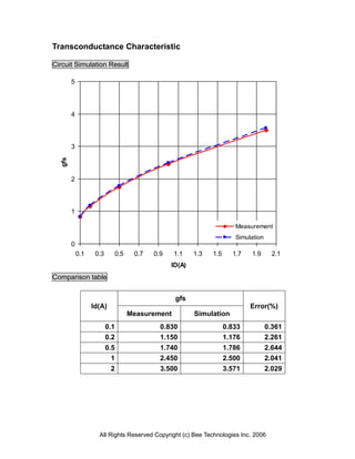
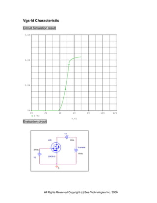
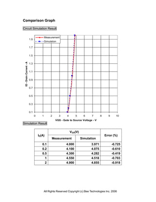
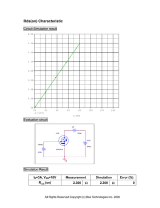
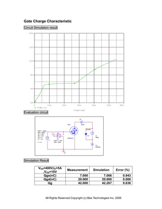
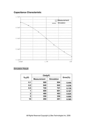
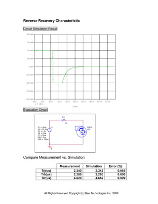
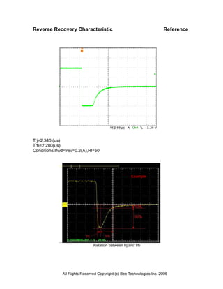
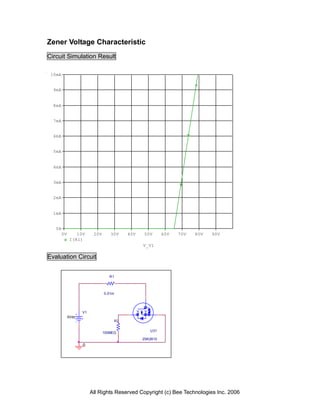
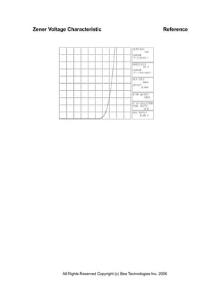

The document is a device modeling report for the power MOSFET part number 2SK2610, manufactured by Toshiba. It includes detailed parameters, simulation results, and measurements related to the device's characteristics such as transconductance, gate charge, capacitance, and switching time. Multiple comparison tables and graphs are provided to showcase the accuracy of simulations against actual measurements.


![Getting Started with Apache Spark: Big Data Made Simple [Free Meetup]](https://cdn.slidesharecdn.com/ss_thumbnails/apachesparkgettingstarted-260203175547-8361bcc3-thumbnail.jpg?width=640&height=640&fit=bounds)


