Downloaded 920 times


![2 Set ATE Configuration @
Inputs Stable
Bi-dir Input Stable
set test_default_period 100
Clock inactive active inactive set test_default_delay 5
set test_default_bidir_delay 55
Output Stable set test_default_strobe 40
Strobe set test_default_strobe_width 0
Period
Specify this default in
Delay synopsys_dc.setup.
Bi-delay
Stobe
2004.08 53
2 Set ATE Configuration @@ -- Create Clock
Default Test Clock:
period test_default_period
1stedge 0.45*test_default_period
2ndedge 0.55*test_default_period
create_test_clock –p 100 –w [list 45 55] clk_RTZ
0 45 55 100
2004.08 54](https://image.slidesharecdn.com/dftbarhouum-111229094428-phpapp02/75/dft-27-2048.jpg)


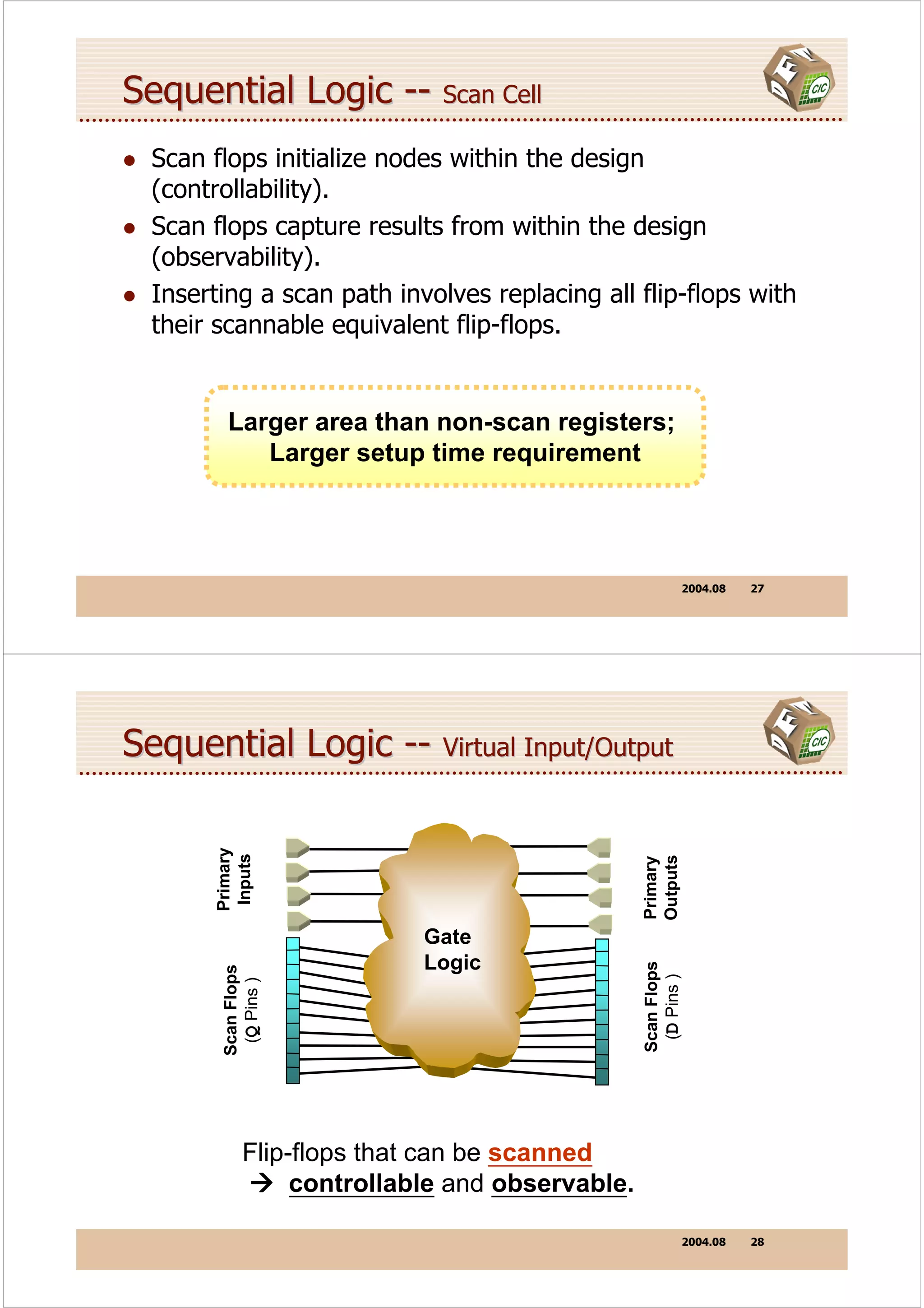
![8 Scan Chain Identification @
When to use?
Import an existing scan design in non-db netlist format. (e.g.,
EDIF, VHDL, Verilog)
Using reset_design after scan chain synthesis. (it will remove
the test attributes from the design)
set_scan_configuration –existing_scan true
2004.08 63
8 Scan Chain Identification @@
Example:
set_scan_configuration -existing_scan true
set_scan_configuration –bidi_mode input
set_signal_type test_scan_in [list SI1 SI2]
set_signal_type test_scan_out [list SO1 SO2]
set_signal_type test_scan_enable SE
check_test
report_test -scan_path
2004.08 64](https://image.slidesharecdn.com/dftbarhouum-111229094428-phpapp02/75/dft-32-2048.jpg)
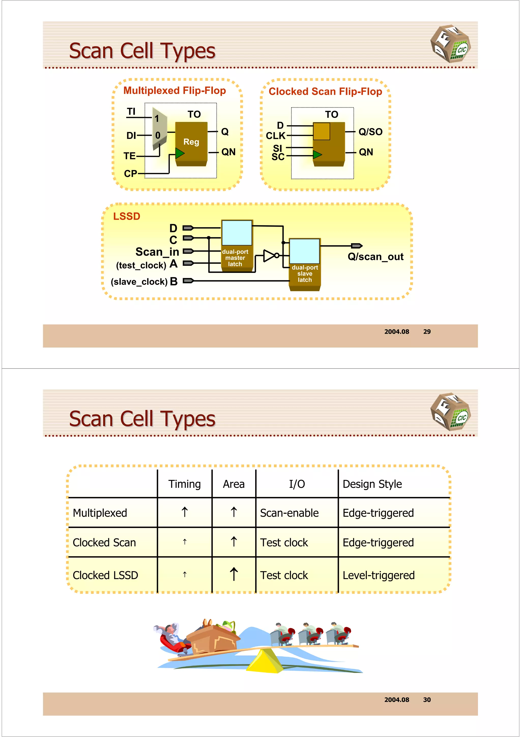
![Block-Level Example @
Scan Ports HIER_BLK
From HDL
SI1 U1 U2 SO1
SI2 SO2
TM
SE
CLK1
CLK2
You are responsible for HIER_BLK, a subdesign on an ASIC.
It has its own hierarchical structure, with two clock domains.
Insert two separate scan chains, and use a test-mode port.
Preview the fault coverage on the post-scan design.
2004.08 67
Block-Level Example @@ TCL script
current_design HIER_BLK
@ compile –scan
@ create_test_clock -p 200 -w [list 90 110] CLK1
@ create_test_clock -p 200 -w [list 120 130] CLK2
set_test_hold 1 TM
@ check_test
set_scan_configuration –chain_count 2
set_scan_configuration –bidi_mode input
set_scan_configuration –clock_mixing no_mix
set_scan_signal test_scan_in –port [list si1 si2]
set_scan_signal test_scan_enable –port SE
set_scan_signal test_scan_out –port [list so1 so2]
preview_scan
@ insert_scan
@ check_test
report_test –scan_path
2004.08 68](https://image.slidesharecdn.com/dftbarhouum-111229094428-phpapp02/75/dft-34-2048.jpg)
![ASIC-Level Example
current_design ASIC
@ create_test_clock -p 200 -w [list 90 110] CLK1
@ create_test_clock -p 200 -w [list 120 130] CLK2
set_test_hold 1 TM
@ set_scan_configuration -existing_scan true
set_scan_configuration -bidi_mode input
@ set_signal_type test_scan_in [list SI1 SI2]
@ set_signal_type test_scan_enable SE
@ set_signal_type test_scan_out [list SO1 SO2]
@ check_test
report_test -scan_path
@ estimate_test_coverage
2004.08 69
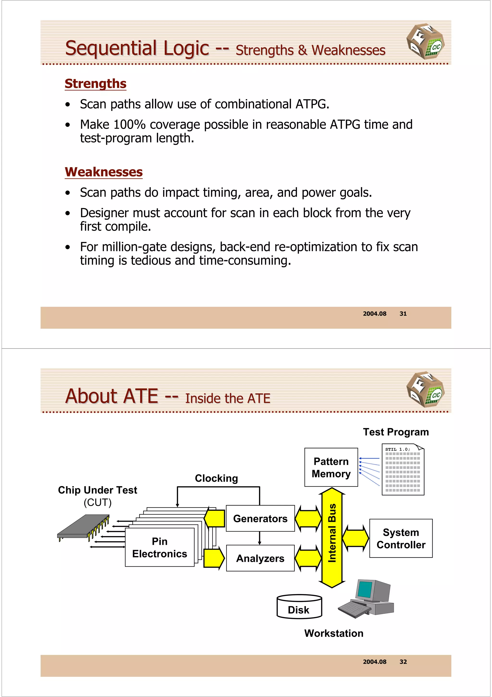
Bottom-Up Synthesis @
Benefits of Bottom-Up Test Synthesis
Complete modules to satisfy design constraints.
Reduce scan synthesis runtime for large designs.
prevent DFT Compiler from renaming the sub-designs of the
CORE.
Tips of Bottom-Up Test Synthesis
Do NOT specify scan signals, mix clock domains.
Switch OFF the insertion of disable logic for multiply-driven nets.
2004.08 70](https://image.slidesharecdn.com/dftbarhouum-111229094428-phpapp02/75/dft-35-2048.jpg)
![Bottom-Up Synthesis @@
current_design A
compile –scan
check_test
set_scan_configuration –disable false
set_scan_configuration –clock_mixing no_mix Synthesized
Blocks
preview_scan Block 1 Block n
insert_scan DFT Check
DFT Check ... DFT Check
check_test
… Scan Chain Synthesis Scan Chain Synthesis
current_design TOP
check_test DFT Check DFT Check
DFT Check
set_scan_configuration –disable true
set_scan_signal test_scan_in –port [list si1 si2] Top-Level
Design
set_scan_signal test_scan_enable –port SE
set_scan_signal test_scan_out –port [list so1 so2]
Top-Level
preview_scan Scan Chain
Synthesis
insert_scan
2004.08 71
Design-for-Testability
Using DFT Compiler
Prevent DFT Violations](https://image.slidesharecdn.com/dftbarhouum-111229094428-phpapp02/75/dft-36-2048.jpg)


![Buffering the Scan-Enable Network
As a rule, the high-fanout scan-enable line should
bebuffered.
Buffering SE is critical for at-speed or transition-delay
testing.
set_scan_signal test_scan_enable -port SE -hookup BUF/Z
Instantiate a clock-tree buffer in the HDL description, or
build a clock-tree for SE.
Use set_dont_touch_network to keep DFTC from
rebuffering.
Route the SE tree to all major blocks.
2004.08 95
Shift Registers @
They are no need to be replaced by Mux-FFs.
set_scan_segment shift -access [list test_scan_in
{dout_reg[1]/D} test_scan_out {dout_reg[7]/Q}]
-contains [list {dout_reg[1]} {dout_reg[2]}
{dout_reg[3]} {dout_reg[4]} {dout_reg[5]}
{dout_reg[6]} {dout_reg[7]}]
set_scan_element false [list {dout_reg[1]}
{dout_reg[2]} {dout_reg[3]} {dout_reg[4]}
{dout_reg[5]} {dout_reg[6]} {dout_reg[7]}]
preview_scan -show segments
insert_scan
2004.08 96](https://image.slidesharecdn.com/dftbarhouum-111229094428-phpapp02/75/dft-48-2048.jpg)


![Bidirectional Ports @@
Inout
F1 ATE
SE
F2
11001010
In TOP module:
set_scan_configuration -disable true
set_scan_configuration –bidi_mode input/output
2004.08 105
Local Control of Tristates and Bidi
set_scan_tristate no_disabling -net TRI3
enable_one Net name
disable_all
set_scan_bidi input -port [list BIDI3 BIDI5]
BIDI5
output Port name
No_disabling
Local control overrides global configuration settings.
2004.08 106](https://image.slidesharecdn.com/dftbarhouum-111229094428-phpapp02/75/dft-53-2048.jpg)


![Custom Scan Path @
set_scan_configuration –chain_count N
DFT Compiler will spilt longest chains into smaller chains.
The scan chains probably will not have equal length.
“Don’t-Lengthen” Option:
Prevents later insertion from
prepending elements to path
set_scan_path CHAIN_4 [list U1 U3 U2] -complete true
String Name: Ordered List:
Uniquely labels this path. List of cell names: flip-flops,
Used later to assign ports. scan links, segments, or blocks..
2004.08 123
Custom Scan Path @@
set_scan_path SCAN_A [list UA/dff*] -complete true
set_scan_path SCAN_B_C [list UB UC/dff1]
insert_scan
HIER_BLOCK
SCAN_A
dff1 dff2 dff1 dff3
UA
dff2 dff4
SCAN_B_C
dff1 dff2 UB
UC
2004.08 124](https://image.slidesharecdn.com/dftbarhouum-111229094428-phpapp02/75/dft-62-2048.jpg)


![Remove Scan Specification
Remove scan specifications made using
set_scan_configuration, set_scan_path,
set_scan_segment, and set_scan_signal
commands:
remove_scan_specification [-all]
[-chain chain_name] [-configuration]
[-segment segment_name] [-signal port_name]
Caution!
reset_design command removes all constraints and
attributes from a design, not just test related constrains
and attributes
2004.08 133
File Output
Create Synthesized Design File
write –hierarchy –format verilog –output ore_syn.v
Create STIL Protocol File (SPF)
write_test_protocol –format stil –out core.spf
2004.08 134](https://image.slidesharecdn.com/dftbarhouum-111229094428-phpapp02/75/dft-67-2048.jpg)


![AutoFix
Commands for specifying the behavior of AutoFix:
1.specifies the types of design 2. exclude a specified
rule violations to fix: list of leaf-level cells
• uncontrollable clock inputs or hierarchical cells
• uncontrollable asynchronous from being fixed by
• preset/clear inputs, or both AutoFix.
1.set_autofix_configuration
2.set_autofix_element
3.set_autofix_clock
3. specify the clock that is connected
to the test points on the designated
parts of the design.
2004.08 139
AutoFix Script
read_file -f verilog TOP.v
current_design TOP
create_test_clock -w [list 45 55] clock
compile -scan
set_dft_configuration -autofix
set_dft_signal test_mode -port test_mode
set_test_hold 1 test_mode
set_autofix_clock CLKA UA
set_autofix_clock CLKB UB
set_autofix_element UC -clock false -async true
preview_dft
insert_dft
check_dft
2004.08 140](https://image.slidesharecdn.com/dftbarhouum-111229094428-phpapp02/75/dft-70-2048.jpg)


![RAM Wrapper Example @
compile -scan
...
create_test_clock -w [list 45 55] ck
set_dft_configuration -shadow_wrapper
set_port_configuration -cell RAM -port "q" -read [list "OEN" 1] -clock ck
set_port_configuration -cell RAM -clock ck
set_port_configuration -cell RAM -port "a" -write [list "WEN" 0] -clock ck
set_port_configuration -cell RAM -port "d" -write [list "WEN" 0] -clock ck
set_wrapper_element RAM_0 -type shadow
preview_dft
insert_dft
compile -incr // for dangling nets (see SOLV-IT! Test-461)
check_dft
...
2004.08 145
RAM Wrapper Example @@
preview_dft
************ Test Point Plan Report ************
Total number of test points : 399
Number of Autofix test points: 0
Number of Wrapper test points: 399
Number of test modes : 1
Number of test point enables : 0
Number of data sources : 128
Number of data sinks : 271
**************************************************
This summary shows that DFT compiler is going to add 399 scan
flip flops to create a shadow wrapper around the RAM.
2004.08 146](https://image.slidesharecdn.com/dftbarhouum-111229094428-phpapp02/75/dft-73-2048.jpg)


![set_testability_configuration
set_testability_configuration
-method tdrv
[-max_observe_point [integer] ]
[-max_observe_logic_area [integer] ]
[-power_saving_on <true/false> ]
Preview scan and observe test point logic
previev_dft –test_points all
Run autofix before TDVR
2004.08 155
DFT Compiler –
Lab 4
Initialization Sequences
& AutoFix](https://image.slidesharecdn.com/dftbarhouum-111229094428-phpapp02/75/dft-78-2048.jpg)


![Log Files and Message Control
Write log message to file:
set message log logfile [-replace | -append]
Turn off displaying log message to transcript:
set message [nodisplay | display]
Stop the comments appearing in the transcript:
set message [-transcript_comments |
-notranscript_comments]
Select message level:
set message [-level expert | standard ]
2004.08 173
Help command
BUILD> help add
Add Atpg Constraints Add Atpg Gates
Add CEll Constraints Add CLocks
Add Equivalent Nofaults Add Faults
Add Net Connections Add Nofaults
Add PI Constraints Add PI Equivalences
Add PO Masks
BUILD> help read netlist
REAd NEtlist <file_name> [-Format <Edif |
VErilog | VHdl>][-Sensitive | -INSensitive]
[-Delete] [-Noabort] [-Verbose]
2004.08 174](https://image.slidesharecdn.com/dftbarhouum-111229094428-phpapp02/75/dft-87-2048.jpg)


![Defining PI constraints
To instruct TetraMAX to hold a port constant during
ATPG pattern generation define a PI constraint:
add pi constraint <held_value> <port_name>
Constraints can also be defined in the SPF file.
Constraints of Z can only be defined for bidirectional or
tri-statable outputs.
2004.08 191
Review the existing constraints
To review the existing list of constraints use:
report pi constraints
To review a list of input, output, bidi, or all ports use
report primitives [- PIS | -POS | -PIOs | -PORts]
2004.08 192](https://image.slidesharecdn.com/dftbarhouum-111229094428-phpapp02/75/dft-96-2048.jpg)


![ATPG Effort: Learn Depth
set atpg –learn N
Default is 0, range: 0-5.
This controls dynamic learning that can occur during
ATPG.
Use of this option may result in excessive CPU time for
high values of learn.
2004.08 205
ATPG Effort: CPU Limit
set atpg –time max_sec_per_fault [max_sec_per_run]
Use 0 to turn off this limit.
Use this option to limit the number of:
CPU seconds spent on a particular fault.
CPU seconds spent on the current “run atpg” command.
2004.08 206](https://image.slidesharecdn.com/dftbarhouum-111229094428-phpapp02/75/dft-103-2048.jpg)


![STIL Procedure File
Standard Test Interface Language IEEE 1450
The STIL Procedure File (SPF) is used to provide the
following information:
scan chain definition
which pins act as “clocks”
timing definitions for pins, clocks, and measures
constrained ports and equivalence relationships
‘test_setup’ macro (test setup sequence)
‘load_unload’ procedure (scan enable sequence)
‘shift’ procedure (scan shift sequence)
The STIL file may also contain pattern data.
2004.08 223
Creating the STIL Procedure File
At any time, a template SPF file can be created with the
command.
write_drc SPF_filename [-replace]
SPF related information can be increased in TetraMAX
by:
add clock <off_state> <port_name>
add pi constraint <held_value> <port_name>
add pi equiv <port_name> [-invert] <port_name>
2004.08 224](https://image.slidesharecdn.com/dftbarhouum-111229094428-phpapp02/75/dft-112-2048.jpg)
![Example: Simple STIL Procedure File
STIL;
STIL header
ScanStructures {…} ScanStructures block
Procedures { Procedures block
load_unload { load_unload procedure
V {…} Shift statement
Shift {…} test_setup macro is optional,
} but may be needed to
} initialize a particular design for
test mode.
MacroDefs {
test_setup {…} res F3
} F1 F2
CLK
2004.08 225
Defining Scan Chains
Scan chains are defined in the ScanStructures block.
ScanStructures {
ScanChain "c1" { ScanIn SDI2; ScanOut SDO2; }
ScanChain "name2" { ScanIn SDI1; ScanOut D1; }
ScanChain "JTAG" { ScanIn TDI; ScanOut TDO; }
ScanChain "chain4" { ScanIn "IRQ[4]"; ScanOut XYZ;}
}
Attention:
uppercase/lowercase
2004.08 226](https://image.slidesharecdn.com/dftbarhouum-111229094428-phpapp02/75/dft-113-2048.jpg)


![Saving Fault Lists
Saving fault lists to a file has many choices. You can
save all faults or just specific classes; select collapsed or
uncollapsed lists; save with or without compression, etc.
2004.08 243
Collapsed V.S. Uncollapsed Faults
TetraMAX processes a collapsed fault list but keeps track
of both the collapsed and uncollapsed faults.
Test Coverage can be reported using either collapsed or
uncollapsed numbers (the default is uncollapsed):
set faults -report [-collapsed | -uncollapsed]
Fault lists can be saved to files or reported in either the
collapsed or uncollapsed form.
write faults filename -all [-collapsed | -uncollapsed]
2004.08 244](https://image.slidesharecdn.com/dftbarhouum-111229094428-phpapp02/75/dft-122-2048.jpg)


![Basic Template*
The basic template for a
module MY_ATPG_RAM ( read, write, data_in, RAM using limited syntax
data_out, read_addr write_addr );
behavioral Verilog.
input read, write;
input [7:0] data_in; // 8 bit data width The port list may vary as
input [3:0] read_addr; // 16 words we define more complicated
input [3:0] write_addr; // 16 words RAMS or ROMS with
output [7:0] data_out; // 8 bit data width
multiple ports, but the
reg [7:0] data_out; // output holding reg
template is essentially the
reg [7:0] memory [0:15] ; // memory storage same.
Note that the ATPG
event WRITE_OP; // event for write-thru
modeling of RAMS requires
...memory port definitions...
that bussed ports be used.
endmodule
2004.08 275
Edge Sensitive Write Ports*
always @(posedge write) begin Example #1: An edge
memory[write_addr] = data_in; sensitive port using rising
#0; ->WRITE_OP;
edge of ‘write’
end
always @(posedge write) if (CS) begin Example #2: An edge
memory[write_addr] = data_in; sensitive write port with
#0; ->WRITE_OP; a qualifier pin of CS.
end
always @(negedge write) if (!CSB) begin
Example #3: A negative
memory[write_addr] = data_in; edge sensitive with an
#0; ->WRITE_OP; active low qualifier pin.
end
Example #4: An edge
and U1 (wen, CS, en2, !en3b);
always @(posedge write) if (wen) begin
sensitive write port with
memory[write_addr] = data_in; complex qualifier.
#0; ->WRITE_OP;
end
2004.08 276](https://image.slidesharecdn.com/dftbarhouum-111229094428-phpapp02/75/dft-138-2048.jpg)
![Level Sensitive Write Ports*
always @(write or write_addr or data_in) Example #1: A level
if (write) begin sensitive write port enabled
memory[write_addr] = data_in; by write=1. Changes on
#0; ->WRITE_OP; address or data with write=1
end update the memory contents.
and U1 (WEN, write, CS, en2, !en3b); Example #2: A level
always @(WEN or write_addr or data_in) sensitive write port with a
if (WEN) begin complex enable.
memory[write_addr] = data_in;
#0; ->WRITE_OP;
end
2004.08 277
Edge Sensitive Read Ports*
always @(posedge read) Example #1: An edge
data_out = memory[read_addr]; sensitive read port controlled
by the rising edge of ‘read.
always @(negedge read) begin
Example #2: An edge
data_out = memory[read_addr];
sensitive read port controlled
end
by the falling edge of ‘read’.
and U1 (RCLK, read, CS, !en2b); Example #3: An edge
always @(posedge RCLK) sensitive read port with a
data_out = memory[read_addr]; complex control.
2004.08 278](https://image.slidesharecdn.com/dftbarhouum-111229094428-phpapp02/75/dft-139-2048.jpg)
![Level Sensitive Read Ports*
always @(read or read_addr or WRITE_OP) Example #1: A level
if (read) data_out = memory[read_addr]; sensitive read port
enabled by read=1.
always @(read or read_addr or WRITE_OP) Changes on address or
if ( read ) data_out = memory[read_addr] data or a write operation
else data_out = 8'bzzzzzzzz; update the memory read
contents.
always @(read or read_addr or WRITE_OP)
if ( read ) data_out = memory[read_addr]
else data_out = 8'b0; Examples #2-#4: A level
sensitive read port with
always @(read or read_addr or WRITE_OP) read port off behavior of
if ( read ) data_out = memory[read_addr] Z, zero, and one,
else data_out = 8'b1111_1111; respectively.
2004.08 279
RAM Modeling: Output Enables*
output [7:0] data_out; Example #1: A level
reg [7:0] data_out, data_reg; /* add data_reg */ sensitive read port
always @(read or read_addr or WRITE_OP)
enabled by read=1 with a
if (read) data_reg = memory[read_addr]; separate tri-state output
enabled by OEB=0..
always @(OEB or data_reg)
if (!OEB) data_out = data_reg;
else data_out = 8'bZZZZZZZZ;
output [7:0] data_out; Examples #2: An edge
reg [7:0] data_out, data_reg; /* add data_reg */ sensitive read port with
and u1 (RCLK, read, CS);
separate tri-state output
always @(posedge RCLK) enabled by OEB=0.
data_reg = memory[read_addr];
always @(OEB or data_reg)
if (!OEB) data_out = data_reg;
else data_out = 8'bZZZZZZZZ;
2004.08 280](https://image.slidesharecdn.com/dftbarhouum-111229094428-phpapp02/75/dft-140-2048.jpg)
![RAM Completed Example*
module ATPG_RAM (CS, OE, read, write, data_in, data_out, addr);
input CS, OE, read, write; input read, write; A completed
input [7:0] data_in; // 8 bit data width example with an
input [3:0] addr; // 16 words
output [7:0] data_out; // module outputs edge controlled
output [7:0] data_reg; // RAM outputs
write port, a
reg [7:0] data_out; // output holding register
reg [7:0] memory [0:15] ; // memory storage level sensitive
.
event WRITE_OP;
read port, and a
and u1 (REN, !read, CS); // form read enable separate output
.
and u2 (TSO, OE, CS); // form tri-state out control
enable.
always @(posedge write) if (CS) begin
memory[addr] = data_in;
#0; ->WRITE_OP;
end
.
always @(REN or addr or WRITE_OP)
if (REN) data_reg = memory[addr]
.
always @(TSO or data_reg)
if (TSO) data_out = data_reg;
else data_out = 8'bzzzzzzzz;
endmodule
2004.08 281
ROM Modeling*
module MY_ROM ( oe, addr, data_out );
A ROM is modeled
input oe; // output control identically to a RAM
input [3:0] addr; // 16 words with these exceptions
output [7:0] data_out; // 8 bits per word it has no write ports
reg [7:0] data_out; // output holding reg it requires an
reg [7:0] memory [0:15] ; // memory storage initialization file
always @(oe or addr)
if (!oe) data_out = memory[addr];
Here's a simple ROM
else data_out = 8'bZZZZZZZZ; with a tri-state output
enable.
initial $readmemh("rom_image.dat", memory);
end module
2004.08 282](https://image.slidesharecdn.com/dftbarhouum-111229094428-phpapp02/75/dft-141-2048.jpg)

![Design-for-Testability
ATPG with TetraMAX
Debugging Problems
Defining Input Masks
Input masks are accomplished by defining a PI
constraint of X on an input.
SETUP> add pi constraints X port_name
To review existing PI masks or delete use:
SETUP> report pi constraints
SETUP> remove pi constraints [ port | -all ]
2004.08 286](https://image.slidesharecdn.com/dftbarhouum-111229094428-phpapp02/75/dft-143-2048.jpg)
![Defining Output Masks
When you do not want to allow the ATPG algorithm to
observe faults through a specific output port.
SETUP> add po masks port_name
To review existing PO masks or delete use:
SETUP> report po masks
SETUP> remove po masks [ port | -all ]
2004.08 287
Scan Cell Masks and Constraints
TetraMAX supports defining constraints on what to load
into a specific scan cell.
By defining an ADD CELL CONSTRAINT command with a
value of 0, 1, or X.
OX - the scan cell will always “Observe X” regardless of the captured value.
XX - the scan cell will always be “Loaded with X and Observed as X”.
2004.08 288](https://image.slidesharecdn.com/dftbarhouum-111229094428-phpapp02/75/dft-144-2048.jpg)


![Creating Black Box Models @@
Synopsys recommends you explicitly define each module
which is to be black boxed so that unintentionally
missing modules are not black boxed.
Set BUIld [ -Black_box <module_name> ]
EX.
set build -reset_boxes
set build -black_box RAM32x8
set build -black_box PLL_BLOCK
set build -bl RAM32x8 -bl PLL_BLOCK
2004.08 303
Creating Empty Box Modules
An “empty box” is similar to a black box with the
exception that its output pins are floating.
Set build [ -empty_box <module_name> ]
EX.
set build -reset_boxes // clears black & empty box list
set build -empty_box BUS_SWITCH
set build -black RAM32x8 -empty IRQ_CORE
2004.08 304](https://image.slidesharecdn.com/dftbarhouum-111229094428-phpapp02/75/dft-152-2048.jpg)


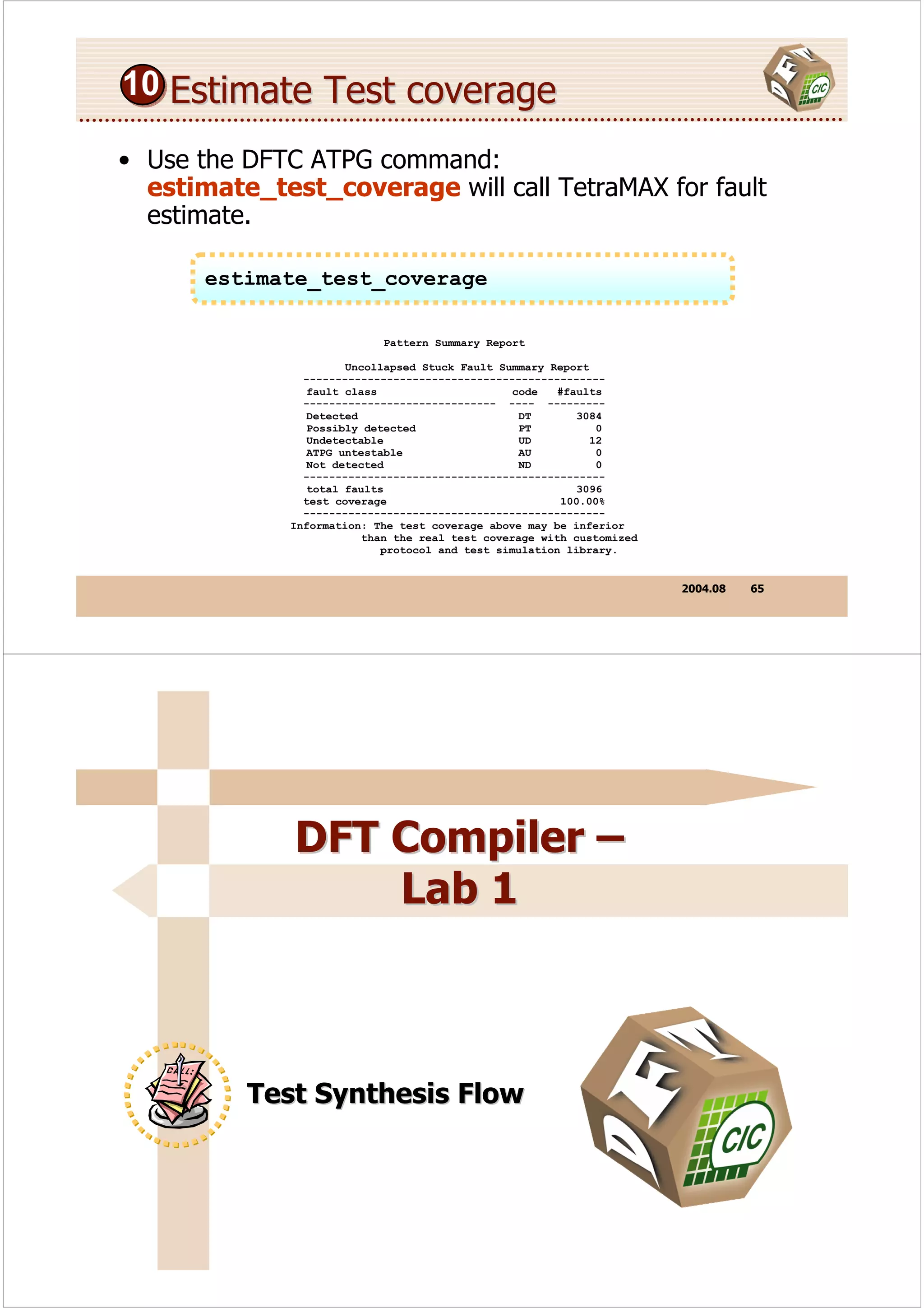
![DFT Compiler Lab 1
1. Go to the directory Lab_1 and invoke DFTC from there.
UNIX> cd lab1
UNIX> design_vision &
Part 1: Top-down basedline flow
2. Read in the FLOW1.db file.
read_file FLOW1.db
3. Perform Scan-Ready Synthesis.
current_design FLOW1
compile –scan
4. Create test clock and constrants. (we have a clock port “CLK”)
ps. If there is a reset port in your design, remember to constraint it in inactive mode.
create_test_clock -period 100 -waveform [list 40 60] [find port "CLK"]
5. Preview the scan synthesis, if it is ok, then insert scan.
preview_scan -show all
insert_scan
6. Check scan rules after scan inserting and report the result.
check_test
report_test -scan_path
7. Run ATPG immediately after scan synthesis.You do not need to specify any additional
scan information since the current_design for ATPG and scan synthesis are the same.
What was the test coverage reported?
estimate_test_coverage
8. See the circuit, what pins have been added?
9. Remove all designs.
remove_design –designs
2004.08 5](https://image.slidesharecdn.com/dftbarhouum-111229094428-phpapp02/75/dft-160-2048.jpg)
![DFT Compiler Lab 1
Part 2: Top-down scan insertion with scan ports sharing
10. Read in the FLOW1.db file.
DFTC> read_file FLOW2.db
11. Perform Scan-Ready Synthesis for design CORE.
Type: include lab1_1.dc . It contains following 4 instructions.
current_design CORE
set_scan_configuration -style multiplexed_flip_flop
set_scan_configuration -methodology full_scan
compile –scan
12. Perform scan synthesis at the top level, FLOW1.
We want to share the following functional ports as scan ports:
scan in: HRS
scan out: SPEAKER OUT
scan enable: TEST_SE
Type: include lab1_2.dc . It contains following 6 instructions.
current_design FLOW1
set_scan_configuration -chain_count 1
create_test_clock -period 100 -waveform [list 40 60] [find port "CLK"]
set_scan_signal test_scan_in -port "HRS"
set_scan_signal test_scan_out -port "SPEAKER_OUT"
set_scan_signal test_scan_enable -port "TEST_SE"
13. Preview the scan synthesis, if it is ok, then insert scan.
preview_scan -show all
insert_scan
14. Check scan rules after scan inserting and report the result.
How many scan chains did you get and how many flip-flops are in each chain?
check_test
report_test -scan_path
15. Run ATPG immediately after scan synthesis.You do not need to specify any additional
scan information since the current_design for ATPG and scan synthesis are the same.
2004.08 6](https://image.slidesharecdn.com/dftbarhouum-111229094428-phpapp02/75/dft-161-2048.jpg)
![DFT Compiler Lab 1
What was the test coverage reported?
estimate_test_coverage
16. Remove all designs.
Remove_design –designs
Part 3: Core-level insertion, Top-level ATPG
17. Read in the FLOW2.db file.
DFTC> read_file FLOW2.db
18. Perform Scan-Ready Synthesis for design CORE.
Type: include lab1_3.dc . It contains following 4 instructions.
current_design CORE
set_scan_configuration -style multiplexed_flip_flop
set_scan_configuration -methodology full_scan
compile –scan
19. Perform scan synthesis for design CORE.
Type: include lab1_4.dc . It contains following 9 instructions.
set_scan_configuration -chain_count 1
create_test_clock -period 100 -waveform [list 40 60] [find port "CLK"]
set_scan_signal test_scan_in -port "HRS"
set_scan_signal test_scan_out -port "SPEAKER_OUT"
set_scan_signal test_scan_enable -port "TEST_SE"
preview_scan -show all
insert_scan
check_test
report_test -scan_path
The design should have one scan chain and the same scan ports as before. That is,
the core-level design has ports with the same names as their corresponding
top-level ports.
2004.08 7](https://image.slidesharecdn.com/dftbarhouum-111229094428-phpapp02/75/dft-162-2048.jpg)
![DFT Compiler Lab 1
20. Change your current design to the top-level design FLOW2 and prepare the design for
ATPG.
Type: include lab1_5.dc . It contains following 6 instructions.
current_design FLOW2
create_test_clock -period 100 -waveform [list 40 60] [find port "CLK"]
set_scan_configuration -existing_scan true
set_signal_type test_scan_in [find port "HRS"]
set_signal_type test_scan_out [find port "SPEAKER_OUT"]
set_signal_type test_scan_enable [find port "TEST_SE"]
21. Run check_test, and if it recognized your single scan chain, proceed with ATPG.
Type: include lab1_6.dc . It contains following 4 instructions.
check_test
report_test -scan_path
estimate_test_coverage
2004.08 8](https://image.slidesharecdn.com/dftbarhouum-111229094428-phpapp02/75/dft-163-2048.jpg)


![DFT Compiler Lab 3
Part 1: Top-down Scan Insertion
1. Go to the directory lab3 and invoke DFTC from there. Read TOP_HIER.db
read_file TOP_HIER.db
current_design TOP_HIER
2. Execute check_test and preview_scan.
check_test
How many clock domains are there in the design? _____________.
preview_scan -show [list scan_clocks cells]
How many scan chain? ______________.
3. Now allow DFTC to mix clock edges within scan chains.
set_scan_configuration -clock_mixing mix_edges
preview_scan -show [list scan_clocks cells]
What is the length of each scan chain? ______________.
4. To get equal length scan chains. -clock_mixing mix_clocks
set_scan_configuration -clock_mixing mix_clocks
set_scan_configuration -chain_count 3
preview_scan -show [list scan_clocks cells]
5. Try NOT insert any lockup latches. Use preview_scan to verify.
set_scan_configuration -add_lockup false
preview_scan -show [list scan_clocks cells]
6. The block ADES contains a 4-bit shift register, which should be declared as a scan
segment to avoid scan replacement of the shift register cells. This will save area.
set_scan_segment shift -access [list test_scan_in instA/sh1_reg/D
test_scan_out instA/sh4_reg/Q] -contains [list "instA/sh*reg"]
set_scan_element false [find cell "sh*_reg"]
preview_scan -show all
7. (Option action)
If you want to change the routing order within scan chains, but you do not like typing
large lists of instances, use the "preview_scan -script" method.
2004.08 13](https://image.slidesharecdn.com/dftbarhouum-111229094428-phpapp02/75/dft-168-2048.jpg)
![DFT Compiler Lab 3
preview_scan -script > scan.scr
then edit scan.scr
include scan.scr
preview_scan -show all
8. By default DFTC generates new ports for use as scan in/enable/out. There are,
however, some exceptions regarding scan out ports. You will now explicitly define
existing ports for use as scan in/enable/out. Please note that the scan enable port
should always be a non-functional port.
Defining Scan Ports:
Type: include lab3_1.dc . It contains following 7 instructions.
set_scan_signal test_scan_in -port {b1[1]} -chain path1
set_scan_signal test_scan_out -port {d1[1]} -chain path1
set_scan_signal test_scan_in -port {b1[2]} -chain path2
set_scan_signal test_scan_out -port {d1[2]} -chain path2
set_scan_signal test_scan_in -port {b1[3]} -chain path3
set_scan_signal test_scan_out -port {d1[3]} -chain path3
set_scan_signal test_scan_enable -port test_se -hookup sebuf/Z
9. Verify your specification using preview_scan.
preview_scan -show all
10. Configuration of bidirectionals.
set_scan_configuration -bidi_mode input
check_test
11. Top-Down Scan insertion.
insert_scan
check_test
report_test -scan_path
estimate_test_coverage
12. Remove all designs.
remove_design -designs
2004.08 14](https://image.slidesharecdn.com/dftbarhouum-111229094428-phpapp02/75/dft-169-2048.jpg)

![DFT Compiler Lab 3
Type: include lab3_3.dc . It contains following 10 instructions.
set_scan_configuration -clock_mixing mix_clocks
set_scan_configuration -chain_count 3
set_scan_configuration -add_lockup false
set_scan_signal test_scan_in -port {b1[1]}
set_scan_signal test_scan_out -port {d1[1]}
set_scan_signal test_scan_in -port {b1[2]}
set_scan_signal test_scan_out -port {d1[2]}
set_scan_signal test_scan_in -port {b1[3]}
set_scan_signal test_scan_out -port {d1[3]}
set_scan_signal test_scan_enable -port test_se
17. Insert scan and check:
insert_scan
check_test
18. Subdesign ADES contains a shift register, which does not need to be scan replaced. In
this step, you will repeat scan insertion with the shift register in block ADES declared
as scan segment.
Type: include lab3_4.dc . It contains following 16 instructions.
remove_design ADES
read_file ADES_GENERIC.db
current_design ADES
set_scan_configuration -style multiplexed_flip_flop
compile -scan
set_scan_element false [find cell "sh*_reg"]
set_scan_segment shift -access [list test_scan_in sh1_reg/D test_scan_out
sh4_reg/Q] -contains [list "sh*_reg"]
check_test
preview_scan -show all
insert_scan
check_test
report_test -scan_path
write -format db -hierarchy -output ADES.db
current_design TOP_ONLY
check_test
2004.08 16](https://image.slidesharecdn.com/dftbarhouum-111229094428-phpapp02/75/dft-171-2048.jpg)


![DFT Compiler Lab 4
and then check_test again. This time you can try to use -verbose option. What kind of
information DFT compiler presents this time?.
remove_test_protocol
read_init_protocol –f stil lab4_init.spf
check_test –verbose
8. Set scan configuration. Use dedicated scan enable (scan_en), scan in and scan out
(user define) and try to minimize chain count.
Type: include lab4_1.dc . It contains following 4 instructions.
set_scan_configuration –clock_mixing mix_edges
set_scan_signal test_scan_enable –port scan_en
set_scan_signal test_scan_in –port din
set_scan_signal test_scan_out -port {Dbus[7]}
9. Preview the scan chain routing. Is it all right?
If OK, then go ahead and implement scan chain routing.
preview_scan –show all
insert_scan
10. Check test (check_test) to find any violations after scan insertion. Is it OK? Also Use
the command (report_test) to see the scan path report.
check_test
report_test –scan_path
11. Estimate fault coverage.
check_test
estimate_test_coverage
12. Write out STIL procedure file (SPF) and synthesized netlist for TetraMAX.
Type: include lab4_2.dc . It contains following 3 instructions.
write –format verilog –hierarchy –output “lab4_dft.v”
write –format db –hierarchy –output “lab4_dft.db”
write_test_protocol –format stil –out “lab4.spf”
13. Remove all designs.
remove_design –designs
2004.08 19](https://image.slidesharecdn.com/dftbarhouum-111229094428-phpapp02/75/dft-174-2048.jpg)


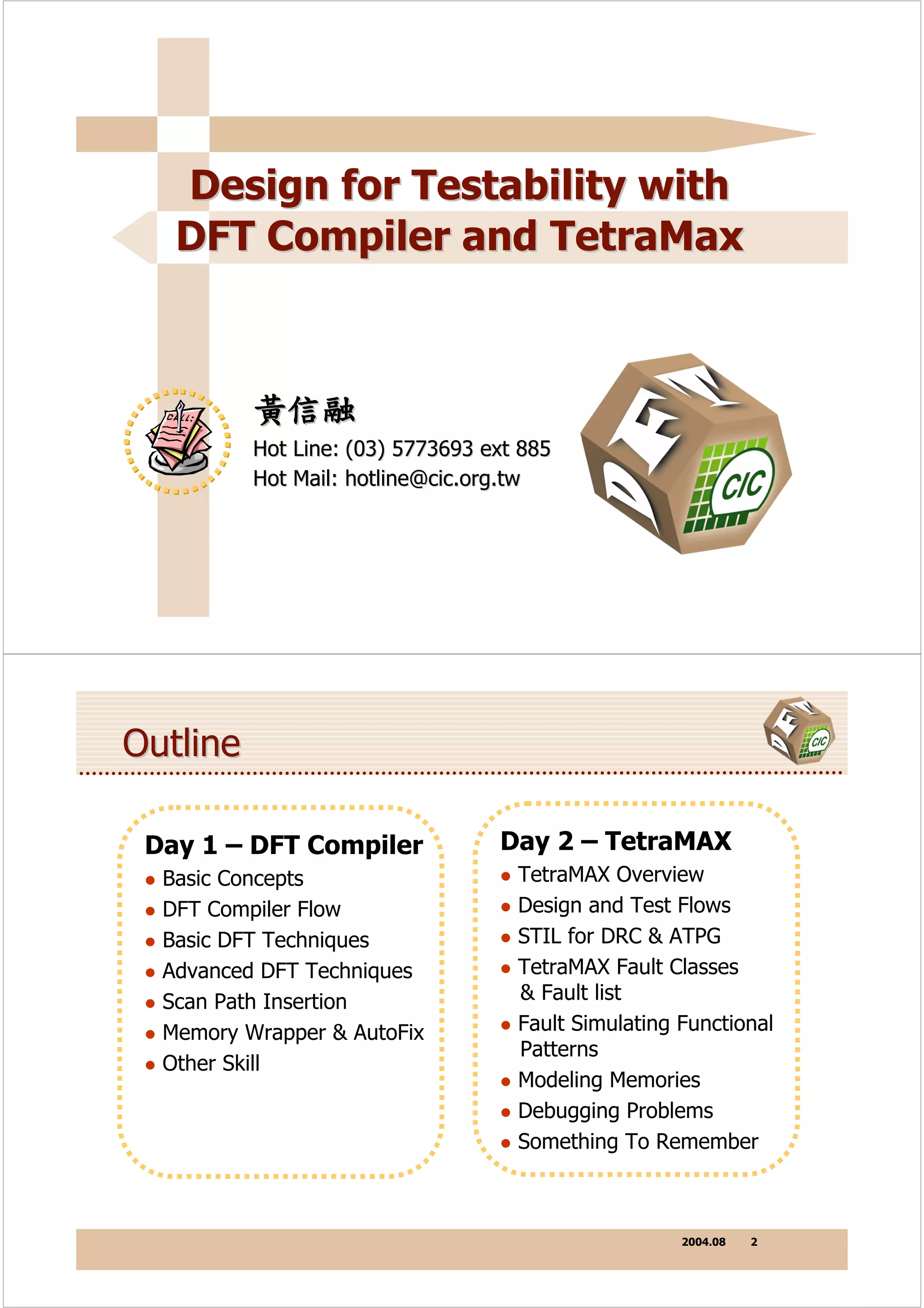
The document discusses a two-day training on design for testability using Synopsys' DFT Compiler and TetraMAX tools. Day 1 covers basic DFT concepts and techniques including scan path insertion and memory wrappers using DFT Compiler. Day 2 focuses on TetraMAX for fault simulation, modeling memories, and debugging problems.

![Design for Test [DFT]-1 (1).pdf DESIGN DFT](https://cdn.slidesharecdn.com/ss_thumbnails/designfortestdft-11-231227151941-28a508a3-thumbnail.jpg?width=640&height=640&fit=bounds)