Mrudang Pujari Resume - ASIC Design Engineer with Expertise in Verilog and SystemVerilog
•
0 likes•42 views

job profile : ASIC design engineer (semiconductor industry)

Recommended
More Related Content
What's hot
What's hot (19)
Similar to Mrudang Pujari Resume - ASIC Design Engineer with Expertise in Verilog and SystemVerilog
Similar to Mrudang Pujari Resume - ASIC Design Engineer with Expertise in Verilog and SystemVerilog (20)
Recently uploaded
Recently uploaded (20)
Mrudang Pujari Resume - ASIC Design Engineer with Expertise in Verilog and SystemVerilog
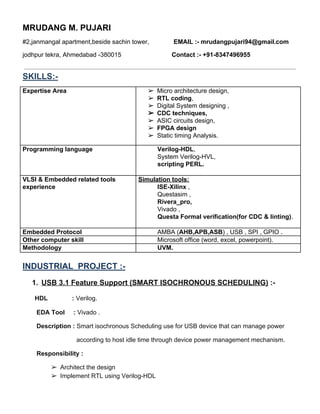
- 1. MRUDANG M. PUJARI #2,janmangal apartment,beside sachin tower, EMAIL :- mrudangpujari94@gmail.com jodhpur tekra, Ahmedabad -380015 Contact :- +91-8347496955 SKILLS:- Expertise Area ➢ Micro architecture design, ➢ RTL coding, ➢ Digital System designing , ➢ CDC techniques, ➢ ASIC circuits design, ➢ FPGA design ➢ Static timing Analysis. Programming language Verilog-HDL, System Verilog-HVL, scripting PERL. VLSI & Embedded related tools experience Simulation tools: ISE-Xilinx , Questasim , Rivera_pro, Vivado , Questa Formal verification(for CDC & linting). Embedded Protocol AMBA (AHB,APB,ASB) , USB , SPI , GPIO . Other computer skill Microsoft office (word, excel, powerpoint). Methodology UVM. INDUSTRIAL PROJECT :- 1. USB 3.1 Feature Support (SMART ISOCHRONOUS SCHEDULING) :- HDL : Verilog. EDA Tool : Vivado . Description : Smart isochronous Scheduling use for USB device that can manage power according to host idle time through device power management mechanism. Responsibility : ➢ Architect the design ➢ Implement RTL using Verilog-HDL
- 2. ➢ Synthesize the design. 2. Bandwidth Calculation Device for USB 3.0 & USB 3.1 :- HDL : Verilog. EDA Tool : Vivado. Description : To calculate actual throughput and USB link utilization with respect to time. Responsibility : ➢ Architect the design . ➢ Implement RTL using Verilog-HDL. ➢ Synthesize the design. INSTITUTIONAL PROJECT :- ❖ AMBA PROTOCOL AHB2APB BRIDGE & ROUTER 1x3 :- HDL : Verilog. HVL : System Verilog. EDA Tool : ISE-Xilinx, Rivera_pro. Description : The router accept data packet on a 8-bit port and route them to one of the three channels : channel 1, channel 2, channel 3. Responsibility :- ➢ Architect the design. ➢ Implement RTL using Verilog-HDL. ➢ Architect class based verification using System Verilog. ➢ Verifies the RTL model using System Verilog. ➢ Generate functional and code coverage for RTL verified sign-off. ➢ Synthesized the design. EDUCATION QUALIFICATION :- S.K.M.S. HIGH SCHOOL , VALSAD GSEB( ) 60.46% 2008STANDARD10TH
- 3. . G.V.D HIGH SCHOOL ,VALSAD GHSEB( )50.60% 2011STANDARD12TH . S.V. NATIONAL INSTITUTE OF TECHNOLOGY,SURAT July -2011 present B.tech (Electronics & communication engineering) CGPA :- 5.48/10.0 2015 . INTERNSHIP :- project intern at Maven Silicon pvt. ltd,Bangalore six month duration in front-end design and verification. July 2015 to February 2016. INDUSTRIAL EXPOSURE :- working as ASIC design engineer at Softnautics pvt. ltd ,Ahmedabad February 2017 to still working (with experience of till Date). DECLARATION :- I hereby declared that above given information is correct as per my knowledge . DATE : Dec 2017 MRUDANG PUJARI9th Place : Ahmedabad