SlideShare a Scribd company logo
1 of 1
Download to read offline
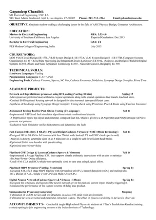
Gagandeep Chandiok
MS Electrical Engineering, USC, LA
949, West Adams Boulevard, Apt# 4, Los Angeles, CA 90007 Phone: (213) 713 -2264 Email:gchandio@usc.edu
OBJECTIVE: Graduate student seeking a challenging career in the field of ASIC/Physical Design, Computer Architecture.
EDUCATION:
Masters in Electrical Engineering GPA: 3.33/4.0
University of Southern California, Los Angeles Expected Graduation: Dec 2015
Bachelor in Electrical Engineering GPA: 4/4
PES Modern College of Engineering, India July 2013
COURSE WORK:
MOS VLSI Circuit Design-EE 477L, VLSI System Design I- EE 577A, VLSI System Design II - EE 577B, Computer Systems
Organization-EE 457, Solid State Processing and Integrated Circuits Laboratory EE 504L, Diagnosis and Design of Reliable Digital
Systems EE658,vMicro and Nano fabrication Technology EE507 , Nano fabrication Lithography EE 508
TECHINICAL SKILLS:
Hardware Languages: Verilog
Programming Languages: C, C++, Perl
Engineering Tools: Cadence Virtuoso, Spectre, NC Sim, Cadence Encounter, Modelsim, Synopsys Design Compiler, Prime Time
ACADEMIC PROJECTS:
Network on Chip Multicore processor using RTL coding (Verilog-NCsim) Spring 15
-Microprocessor performs basic arithmetic, logical operations along with special operations like branch, load and store.
-Cardinal Bi-Directional Routing network is designed for data traversal between different cores
-Synthesis of the design using Synopsys Design Compiler, Timing check using Primetime, Place & Route using Cadence Encounter
Automated Testing Tool for Post Silicon Testing (C Language): Fall 14
-Implemented ATPG and fault simulator algorithms to test combinational circuits.
-A Preprocessor levels the circuit and generates collapsed fault list, which is given to a D Algorithm and PODEM based ATPG to
generate test patterns.
-Deductive Fault Simulator verifies test patterns and determines the fault
Full-Custom 1024-Bit 6-T SRAM- Physical Design Cadence-Virtuoso (TSMC 180nm Technology) Fall 14
-Designed 1K bit SRAM in full custom with four 256-bit wide banks (LVS and DRC checks performed)
-Analysis is done to determine sizes of all 6 transistors in a single bit cell for efficient Read/Write.
-Optimized 16-bit row decoder with pre-decoding.
-Optimized area*power*delay
Pipelined CPU Design & Layout (Cadence Spectre & Virtuoso) Fall 14
-Implemented a 5 stage Pipelined CPU that supports simple arithmetic instructions with an aim to optimize
the Area*Power*Delay efficiency.
-Used 16 bit CLA and RCA which were optimally sized to save area using Logical effort.
Pipelined MIPS Processor (Verilog- Modelsim) Spring 14
-Designed RTL of a 5 stage MIPS pipeline with forwarding unit (FU), hazard detection (HDU) and stalling unit.
-RTL Design of ALU, Single Cycle CPU and Multi-Cycle CPU.
Digital Neuron Network (Cadence Spectre & Virtuoso - 180nm) Spring 14
-Designed the schematic and layout of the neuron network given the past and current inputs thereby triggering it.
-Measured the performance of the system in terms of delay area product.
Semiconductor Processing Laboratory Ongoing
-Fabrication of CMOS devices and test structures in a class 100 clean room environment.
-Fabricated devices are tested and parameter extraction is done. The effect of process variability on devices is observed.
ACCOMPLISHMENT’S- Coached & taught High school Physics to students at IITian’s Prashikshan Kendra (training
center) aspiring to join engineering streams at the Indian Institute of Technology.

More Related Content

What's hot

What's hot (20)

Asic vs fpga
Asic vs fpgaAsic vs fpga
Asic vs fpga
 
The comparison between FPGA , ARDUINO , ASIC
The comparison between FPGA , ARDUINO , ASIC The comparison between FPGA , ARDUINO , ASIC
The comparison between FPGA , ARDUINO , ASIC
 
Chandan Kumar_3+_Years _EXP
Chandan Kumar_3+_Years _EXPChandan Kumar_3+_Years _EXP
Chandan Kumar_3+_Years _EXP
 
Introduction to proteus
Introduction to  proteusIntroduction to  proteus
Introduction to proteus
 
Asic
AsicAsic
Asic
 
Reconfigurable ICs
Reconfigurable ICsReconfigurable ICs
Reconfigurable ICs
 
ASIC
ASICASIC
ASIC
 
Making of an Application Specific Integrated Circuit
Making of an Application Specific Integrated CircuitMaking of an Application Specific Integrated Circuit
Making of an Application Specific Integrated Circuit
 
ASIC DESIGN FLOW
ASIC DESIGN FLOWASIC DESIGN FLOW
ASIC DESIGN FLOW
 
Chandan Kumar_3+_Years _EXP
Chandan Kumar_3+_Years _EXPChandan Kumar_3+_Years _EXP
Chandan Kumar_3+_Years _EXP
 
ASIC vs FPGA
ASIC vs FPGAASIC vs FPGA
ASIC vs FPGA
 
Fpga & VHDL
Fpga & VHDLFpga & VHDL
Fpga & VHDL
 
SoC: System On Chip
SoC: System On ChipSoC: System On Chip
SoC: System On Chip
 
FPGA Architecture Presentation
FPGA Architecture PresentationFPGA Architecture Presentation
FPGA Architecture Presentation
 
Nikita Resume
Nikita ResumeNikita Resume
Nikita Resume
 
Fpga
FpgaFpga
Fpga
 
Asic design lect1 2 august 28 2012
Asic design lect1 2 august 28 2012Asic design lect1 2 august 28 2012
Asic design lect1 2 august 28 2012
 
Tutorial on FPGA Routing
Tutorial on FPGA RoutingTutorial on FPGA Routing
Tutorial on FPGA Routing
 
Fpga optimus main_print
Fpga optimus  main_printFpga optimus  main_print
Fpga optimus main_print
 
Traditional vs. SoC FPGA Design Flow A Video Pipeline Case Study
Traditional vs. SoC FPGA Design Flow A Video Pipeline Case StudyTraditional vs. SoC FPGA Design Flow A Video Pipeline Case Study
Traditional vs. SoC FPGA Design Flow A Video Pipeline Case Study
 

Similar to MS Electrical Engineer Seeking ASIC/Physical Design Career

Similar to MS Electrical Engineer Seeking ASIC/Physical Design Career (20)

Resume
ResumeResume
Resume
 
New_resume_v2
New_resume_v2New_resume_v2
New_resume_v2
 
Sudheer vaddi Resume
Sudheer vaddi ResumeSudheer vaddi Resume
Sudheer vaddi Resume
 
Resume
ResumeResume
Resume
 
Resume_Aney N Khatavkar
Resume_Aney N KhatavkarResume_Aney N Khatavkar
Resume_Aney N Khatavkar
 
Resume_Aney N Khatavkar
Resume_Aney N KhatavkarResume_Aney N Khatavkar
Resume_Aney N Khatavkar
 
Chandan Kumar_3+_Years _EXP
Chandan Kumar_3+_Years _EXPChandan Kumar_3+_Years _EXP
Chandan Kumar_3+_Years _EXP
 
resume
resumeresume
resume
 
Chadalavada, Divya Sai
Chadalavada, Divya SaiChadalavada, Divya Sai
Chadalavada, Divya Sai
 
CV-A Naeem
CV-A NaeemCV-A Naeem
CV-A Naeem
 
LTTS_Dinesh Prasath_Resume
LTTS_Dinesh Prasath_ResumeLTTS_Dinesh Prasath_Resume
LTTS_Dinesh Prasath_Resume
 
VISHNU POREDDY Resume
VISHNU POREDDY ResumeVISHNU POREDDY Resume
VISHNU POREDDY Resume
 
CHANDAN RESUME
CHANDAN RESUMECHANDAN RESUME
CHANDAN RESUME
 
Sagar_Patil_Resume
Sagar_Patil_ResumeSagar_Patil_Resume
Sagar_Patil_Resume
 
Sabareesh_Sridhar_resume
Sabareesh_Sridhar_resumeSabareesh_Sridhar_resume
Sabareesh_Sridhar_resume
 
Mirabilis_Design AMD Versal System-Level IP Library
Mirabilis_Design AMD Versal System-Level IP LibraryMirabilis_Design AMD Versal System-Level IP Library
Mirabilis_Design AMD Versal System-Level IP Library
 
ARVIND_BALAKUMAR_Resume
ARVIND_BALAKUMAR_ResumeARVIND_BALAKUMAR_Resume
ARVIND_BALAKUMAR_Resume
 
Resume Dhananjay Gowda
Resume Dhananjay GowdaResume Dhananjay Gowda
Resume Dhananjay Gowda
 
Resume
ResumeResume
Resume
 
Varun Gatne - Resume - Final
Varun Gatne - Resume - FinalVarun Gatne - Resume - Final
Varun Gatne - Resume - Final
 

MS Electrical Engineer Seeking ASIC/Physical Design Career

  • 1. Gagandeep Chandiok MS Electrical Engineering, USC, LA 949, West Adams Boulevard, Apt# 4, Los Angeles, CA 90007 Phone: (213) 713 -2264 Email:gchandio@usc.edu OBJECTIVE: Graduate student seeking a challenging career in the field of ASIC/Physical Design, Computer Architecture. EDUCATION: Masters in Electrical Engineering GPA: 3.33/4.0 University of Southern California, Los Angeles Expected Graduation: Dec 2015 Bachelor in Electrical Engineering GPA: 4/4 PES Modern College of Engineering, India July 2013 COURSE WORK: MOS VLSI Circuit Design-EE 477L, VLSI System Design I- EE 577A, VLSI System Design II - EE 577B, Computer Systems Organization-EE 457, Solid State Processing and Integrated Circuits Laboratory EE 504L, Diagnosis and Design of Reliable Digital Systems EE658,vMicro and Nano fabrication Technology EE507 , Nano fabrication Lithography EE 508 TECHINICAL SKILLS: Hardware Languages: Verilog Programming Languages: C, C++, Perl Engineering Tools: Cadence Virtuoso, Spectre, NC Sim, Cadence Encounter, Modelsim, Synopsys Design Compiler, Prime Time ACADEMIC PROJECTS: Network on Chip Multicore processor using RTL coding (Verilog-NCsim) Spring 15 -Microprocessor performs basic arithmetic, logical operations along with special operations like branch, load and store. -Cardinal Bi-Directional Routing network is designed for data traversal between different cores -Synthesis of the design using Synopsys Design Compiler, Timing check using Primetime, Place & Route using Cadence Encounter Automated Testing Tool for Post Silicon Testing (C Language): Fall 14 -Implemented ATPG and fault simulator algorithms to test combinational circuits. -A Preprocessor levels the circuit and generates collapsed fault list, which is given to a D Algorithm and PODEM based ATPG to generate test patterns. -Deductive Fault Simulator verifies test patterns and determines the fault Full-Custom 1024-Bit 6-T SRAM- Physical Design Cadence-Virtuoso (TSMC 180nm Technology) Fall 14 -Designed 1K bit SRAM in full custom with four 256-bit wide banks (LVS and DRC checks performed) -Analysis is done to determine sizes of all 6 transistors in a single bit cell for efficient Read/Write. -Optimized 16-bit row decoder with pre-decoding. -Optimized area*power*delay Pipelined CPU Design & Layout (Cadence Spectre & Virtuoso) Fall 14 -Implemented a 5 stage Pipelined CPU that supports simple arithmetic instructions with an aim to optimize the Area*Power*Delay efficiency. -Used 16 bit CLA and RCA which were optimally sized to save area using Logical effort. Pipelined MIPS Processor (Verilog- Modelsim) Spring 14 -Designed RTL of a 5 stage MIPS pipeline with forwarding unit (FU), hazard detection (HDU) and stalling unit. -RTL Design of ALU, Single Cycle CPU and Multi-Cycle CPU. Digital Neuron Network (Cadence Spectre & Virtuoso - 180nm) Spring 14 -Designed the schematic and layout of the neuron network given the past and current inputs thereby triggering it. -Measured the performance of the system in terms of delay area product. Semiconductor Processing Laboratory Ongoing -Fabrication of CMOS devices and test structures in a class 100 clean room environment. -Fabricated devices are tested and parameter extraction is done. The effect of process variability on devices is observed. ACCOMPLISHMENT’S- Coached & taught High school Physics to students at IITian’s Prashikshan Kendra (training center) aspiring to join engineering streams at the Indian Institute of Technology.