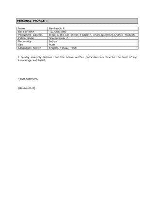
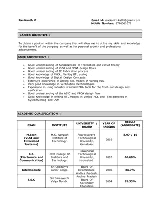
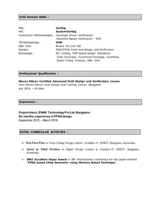
Ravikanth P Email id: ravikanth.katti@gmail.com
Mobile Number: 8746061678
CAREER OBJECTIVE :
To obtain a position within the company that will allow me to utilize my skills and knowledge
for the benefit of the company as well as for personal growth and professional
advancement.
CORE COMPETENCY :
 Good understanding of fundamentals of Transistors and circuit theory
 Good understanding of VLSI and FPGA design flows
 Good understanding of IC Fabrication process
 Good knowledge of VHDL, Verilog RTL coding
 Good knowledge of Digital Design Concepts
 Extensive experience in writing RTL models in Verilog HDL
 Very good knowledge in verification methodologies
 Experience in using industry standard EDA tools for the front-end design and
verification
 Good understanding of the ASIC and FPGA design flow
 Good Knowledge in writing RTL models in Verilog HDL and Test benches in
SystemVerilog and UVM
ACADEMIC QUALIFICATION :
EXAM INSTITUTE
UNIVERSITY /
BOARD
YEAR OF
PASSING
RESULT
(AGGREGATE)
M.Tech
(VLSI and
Embedded
Systems)
M.S. Ramaiah
Institute of
Technology.
Visvesvaraya
Technological
University,
Karnataka.
2016
8.97 / 10
B.E.
(Electronics and
Communication)
CMR College Of
Institute and
Technology.
Jawaharlal
Technological
University,
Hyderabad.
2010 66.60%
Intermediate
Sri Chaitanya
Junior Collge.
Board Of
Intermediate,
Andhra Pradesh.
2006 86.7%
S.S.C
Sri Saraswathi
Vidya Mandir.
Andhra Pradesh
Board Of
Secondary
Education.
2004 85.33%
HDL: Verilog
HVL: SystemVerilog
Verification Methodologies: Coverage Driven Verification
Assertion Based Verification - SVA
TB Methodology: UVM
EDA Tool: Riviera Pro and ISE
Domain: ASIC/FPGA front-end Design and Verification
Knowledge: RTL Coding, FSM based design, Simulation,
Code Coverage, Functional Coverage, Synthesis,
Static Timing Analysis, ABV- SVA
Maven Silicon Certified Advanced VLSI Design and Verification course
from Maven Silicon VLSI Design and Training Center, Bangalore
july 2016 – till date
Project Intern, EWAS TechnologyPvt.Ltd, Bangalore.
Six months experience in FPGAdesign
September 2015 – March 2016
EXTRA CURRICULAR ACTIVTIES :
 Won First Prize in Texas Analog Design contest –Avishkar-15, MSRIT, Bangalore, Karnataka.
 Stood in Third Position in Digital Design Contest in Avishkar-15, MSRIT, Bangalore,
Karnataka.
 IRAJ Excellent Paper Award in IRF international conference for the paper entitled
“FPGA based Chirp Generator using Memory Based Technique”.
VLSI Domain Skills :
Professional Qualification :
Experience :
ACADEMIC PROJECTS :
[1] Router 1x3 – RTL design and Verification
HDL: Verilog
HVL: SystemVerilog
EDA Tools: ISE
Description: The router accepts data packets on a single 8-bit port and routes them to one
of the three output channels, channel0, channel1 and channel2.An error detection technique
that test the integrity of digital data being transmitted between Server & Client. This
technique ensures that the data transmitted by the Server network is received by the Client
network without getting corrupted. Active low synchronous input signal that resets the
router. Under reset condition, the router FIFOs are made empty and the valid out signals
goes low indicating that no valid packet is detected on the output data bus. Sending and
Reading Packet will done according to the Protocol.
Responsibilities:
 Architected the design
 Implemented RTL using Verilog HDL.
 Architected the class based verification environment using system Verilog
 Verified the RTL model using SystemVerilog.
 Generated functional and code coverage for the RTL verification sign-off
 Synthesized the design
[2] Chirp Generator using Direct Digital Synthesizer and Memory based technique
HDL: Verilog
EDA Tool: ISE
Description: The Project aims at generation of 16-bit precision Digital Chirp Signal using
FPGA & Verilog. The generation of chirp signal is done by using two commonly known
methods DDS and Memory Based Technique. DDS and Memory Based Technique implement
Look Up Table Method. Depends on the address generated by the phase generator the
sinusoidal sample extracted from look up table. The sample will fed to the DAC to get
analog signal.
Responsibilities:
 Architected the design.
 Implemented RTL using Verilog HDL.
 Verified RTL model using isim simulator.
 Synthesized the design.
 Interfacing the design with DAC.
[3].Implementation of 64-bit Kogge-Stone adder in verilog with delay comparison
to ripple carry adder
HDL: Verilog
EDA Tool : Xilinx ISE
Description: Area timing analysis and comparison for 64-bit Kogge-Stone adder and 64-bit
ripple carry adder and constructing a hybrid adder with 32-bit Kogge-Stone and 32-bit
ripple carry adder.
Responsibilities: To write a Verilog code using generates statements for 64-bit Kogge-
Stone adder to produce observable delays in the simulation window.
[4].Parking Assistance Using Ultrasonic Sensor
Programming language: C
Hardware: Arduino, Ultrasonic Sensor
Description: The problem occurs during parking vehicle can be overcome by using
"ULTRASONIC SENSOR ". The sensor calculates how far the obstacle will be and gives the
information in LCD display to the driver.
Responsibilities: To write C programming language and interface ultrasonic sensor with
Arduino.
[5]. Home Automation
Programming Language: C
Hardware: Arduino
Description: The basic idea of home automation is controlling home appliances such as
Fan, Light, A/C, Water Heater etc. which are under same network either by voice or by text
messages.
Responsibilities: To write C programming language, interface sensor with Arduino and
establish communication between mobile and the Arduino.
[6]. Live Human Detection Using PIR Sensor
Programming Language: C
Hardware: Microcontroller
Description: Project is robot surveillance system which includes PIR sensor which detects
heat radiations coming from live human body.
Responsibilities: To write C programming language, interface sensor with Microcontroller
and establish communication between remote controller and the microcontroller
PERSONAL PROFILE :
Name Ravikanth P
Date of Birth 12/June/1989
Permanent address D-No 7/354,Car Street, Tadipatri, Anantapur(Dist).Andhra Pradesh.
Father Name Sreenivasulu P
Nationality Indian
Sex Male
Languages Known English, Telugu, Hindi
I hereby solemnly declare that the above written particulars are true to the best of my
knowledge and belief.
Yours faithfully,
(Ravikanth.P)

Ravikanth Resume

  • 1.
    Ravikanth P Emailid: ravikanth.katti@gmail.com Mobile Number: 8746061678 CAREER OBJECTIVE : To obtain a position within the company that will allow me to utilize my skills and knowledge for the benefit of the company as well as for personal growth and professional advancement. CORE COMPETENCY :  Good understanding of fundamentals of Transistors and circuit theory  Good understanding of VLSI and FPGA design flows  Good understanding of IC Fabrication process  Good knowledge of VHDL, Verilog RTL coding  Good knowledge of Digital Design Concepts  Extensive experience in writing RTL models in Verilog HDL  Very good knowledge in verification methodologies  Experience in using industry standard EDA tools for the front-end design and verification  Good understanding of the ASIC and FPGA design flow  Good Knowledge in writing RTL models in Verilog HDL and Test benches in SystemVerilog and UVM ACADEMIC QUALIFICATION : EXAM INSTITUTE UNIVERSITY / BOARD YEAR OF PASSING RESULT (AGGREGATE) M.Tech (VLSI and Embedded Systems) M.S. Ramaiah Institute of Technology. Visvesvaraya Technological University, Karnataka. 2016 8.97 / 10 B.E. (Electronics and Communication) CMR College Of Institute and Technology. Jawaharlal Technological University, Hyderabad. 2010 66.60% Intermediate Sri Chaitanya Junior Collge. Board Of Intermediate, Andhra Pradesh. 2006 86.7% S.S.C Sri Saraswathi Vidya Mandir. Andhra Pradesh Board Of Secondary Education. 2004 85.33%
  • 2.
    HDL: Verilog HVL: SystemVerilog VerificationMethodologies: Coverage Driven Verification Assertion Based Verification - SVA TB Methodology: UVM EDA Tool: Riviera Pro and ISE Domain: ASIC/FPGA front-end Design and Verification Knowledge: RTL Coding, FSM based design, Simulation, Code Coverage, Functional Coverage, Synthesis, Static Timing Analysis, ABV- SVA Maven Silicon Certified Advanced VLSI Design and Verification course from Maven Silicon VLSI Design and Training Center, Bangalore july 2016 – till date Project Intern, EWAS TechnologyPvt.Ltd, Bangalore. Six months experience in FPGAdesign September 2015 – March 2016 EXTRA CURRICULAR ACTIVTIES :  Won First Prize in Texas Analog Design contest –Avishkar-15, MSRIT, Bangalore, Karnataka.  Stood in Third Position in Digital Design Contest in Avishkar-15, MSRIT, Bangalore, Karnataka.  IRAJ Excellent Paper Award in IRF international conference for the paper entitled “FPGA based Chirp Generator using Memory Based Technique”. VLSI Domain Skills : Professional Qualification : Experience :
  • 3.
    ACADEMIC PROJECTS : [1]Router 1x3 – RTL design and Verification HDL: Verilog HVL: SystemVerilog EDA Tools: ISE Description: The router accepts data packets on a single 8-bit port and routes them to one of the three output channels, channel0, channel1 and channel2.An error detection technique that test the integrity of digital data being transmitted between Server & Client. This technique ensures that the data transmitted by the Server network is received by the Client network without getting corrupted. Active low synchronous input signal that resets the router. Under reset condition, the router FIFOs are made empty and the valid out signals goes low indicating that no valid packet is detected on the output data bus. Sending and Reading Packet will done according to the Protocol. Responsibilities:  Architected the design  Implemented RTL using Verilog HDL.  Architected the class based verification environment using system Verilog  Verified the RTL model using SystemVerilog.  Generated functional and code coverage for the RTL verification sign-off  Synthesized the design [2] Chirp Generator using Direct Digital Synthesizer and Memory based technique HDL: Verilog EDA Tool: ISE Description: The Project aims at generation of 16-bit precision Digital Chirp Signal using FPGA & Verilog. The generation of chirp signal is done by using two commonly known methods DDS and Memory Based Technique. DDS and Memory Based Technique implement Look Up Table Method. Depends on the address generated by the phase generator the sinusoidal sample extracted from look up table. The sample will fed to the DAC to get analog signal. Responsibilities:  Architected the design.  Implemented RTL using Verilog HDL.  Verified RTL model using isim simulator.  Synthesized the design.  Interfacing the design with DAC.
  • 4.
    [3].Implementation of 64-bitKogge-Stone adder in verilog with delay comparison to ripple carry adder HDL: Verilog EDA Tool : Xilinx ISE Description: Area timing analysis and comparison for 64-bit Kogge-Stone adder and 64-bit ripple carry adder and constructing a hybrid adder with 32-bit Kogge-Stone and 32-bit ripple carry adder. Responsibilities: To write a Verilog code using generates statements for 64-bit Kogge- Stone adder to produce observable delays in the simulation window. [4].Parking Assistance Using Ultrasonic Sensor Programming language: C Hardware: Arduino, Ultrasonic Sensor Description: The problem occurs during parking vehicle can be overcome by using "ULTRASONIC SENSOR ". The sensor calculates how far the obstacle will be and gives the information in LCD display to the driver. Responsibilities: To write C programming language and interface ultrasonic sensor with Arduino. [5]. Home Automation Programming Language: C Hardware: Arduino Description: The basic idea of home automation is controlling home appliances such as Fan, Light, A/C, Water Heater etc. which are under same network either by voice or by text messages. Responsibilities: To write C programming language, interface sensor with Arduino and establish communication between mobile and the Arduino. [6]. Live Human Detection Using PIR Sensor Programming Language: C Hardware: Microcontroller Description: Project is robot surveillance system which includes PIR sensor which detects heat radiations coming from live human body. Responsibilities: To write C programming language, interface sensor with Microcontroller and establish communication between remote controller and the microcontroller
  • 5.
    PERSONAL PROFILE : NameRavikanth P Date of Birth 12/June/1989 Permanent address D-No 7/354,Car Street, Tadipatri, Anantapur(Dist).Andhra Pradesh. Father Name Sreenivasulu P Nationality Indian Sex Male Languages Known English, Telugu, Hindi I hereby solemnly declare that the above written particulars are true to the best of my knowledge and belief. Yours faithfully, (Ravikanth.P)