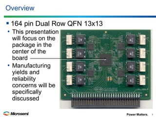
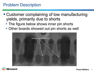
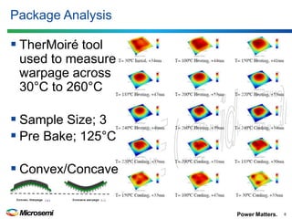
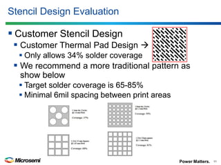
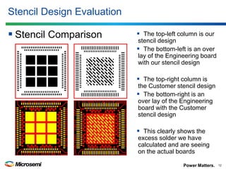
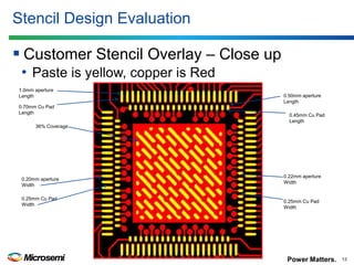
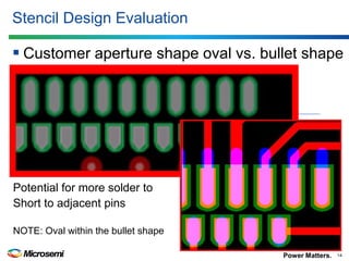
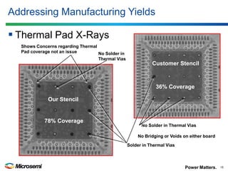
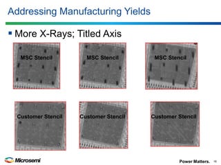
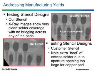
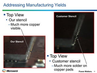
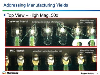
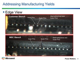
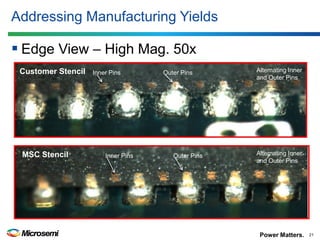
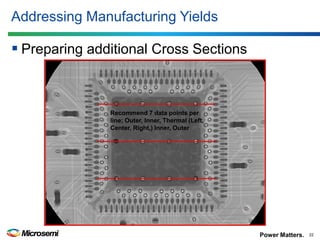
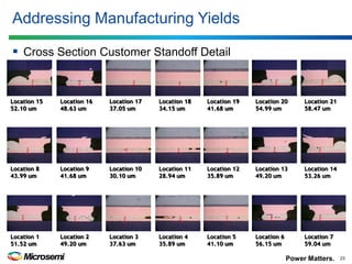
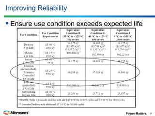
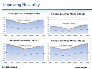
Power Matters 
Understanding the Criticality of Stencil Aperture Design and Implementation for a QFN Package 
Larry Bright & Greg Caswell 
November 2013
Power Matters. 
Agenda 
Overview 
Problem Description 
Analysis 
Stencil Design 
Addressing Manufacturing Yields 
Improving Reliability 
PCB and Stencil Recommendations 
Discussion 
Conclusion 
2
Power Matters. 
Overview 
164 pin Dual Row QFN 13x13 
3 
•This presentation will focus on the package in the center of the board 
•Manufacturing yields and reliability concerns will be specifically discussed
Power Matters. 
Problem Description 
Customer complaining of low manufacturing yields, primarily due to shorts 
•The figure below shows inner pin shorts 
•Other boards showed out pin shorts as well 
4 
Bridging (shorts) between pins
Power Matters. 
Analysis 
Initial evaluation on the package itself 
•Package warpage measurements 
Limited data on Customer board design 
•Cross Sectional analysis performed to determine 
–Extent and location of shorts 
–Via structure and solder escape paths 
–Standoff height 
5 
2.46 2.30 1.66 1.53 1.64 2.03 2.16 0.501.001.502.002.503.00OuterInnerThermalThermalThermalInnerOuterMSC Bond-line profile - Top 2.05 1.91 1.46 1.34 1.64 2.16 2.30 0.501.001.502.002.503.00OuterInnerThermalThermalThermalInnerOuterCustomer Bond-line profile - Top
Power Matters. 
Package Analysis 
6 
TherMoiré tool used to measure warpage across 30°C to 260°C 
Sample Size; 3 
Pre Bake; 125°C 
Convex/Concave
Power Matters. 
Package Analysis 
 Package warpage measurements 
• Package within 50um spec across temperature 
7
Power Matters. 
Cross-Sectional Analysis 
Bridging across outer leads causing shorts 
•Bridging was identified in five locations (fours sets of bridged leads) see red arrows and numbers 
8
Power Matters. 
Cross-Sectional Analysis 
No solder wicking into the Thermal Vias 
•Supposition is that the QFN reached reflow temperature before the PCB 
•Thermal via holes ~19mils (larger then desired) 
•No indication of any via filled material 
•No tenting at bottom or top 
9
Power Matters. 
Cross-Sectional Analysis 
Bond line thickness measurements 
10 
Center Cross Sections (Thermal Pad and 2 Leads) Bond-line Thickness Measurements 
Board ID 
Part ID 
Left Lead (Outer) 
Left Lead (Inner) 
Thermal Pad 
Right Lead (Inner) 
Right Lead (Outer) 
Manufacturing 
A24 
1.73 
1.38 
1.14 
1.46 
1.65 
Manufacturing 
A21 
1.65 
1.54 
1.10 
1.34 
1.54 
Evaluation 
U2 
2.20 
N/A 
1.30 
N/A 
2.28 
•Thermal pad standoff ~29um (1.14 mils) 
•Not meeting IPC target of 2.5-3.0 mils 
•Data shows package concave profile
Power Matters. 
Stencil Design Evaluation 
Customer Stencil Design 
Customer Thermal Pad Design  
Only allows 34% solder coverage 
We recommend a more traditional pattern as show below 
Target solder coverage is 65-85% 
Minimal 6mil spacing between print areas 
11
Power Matters. 
Stencil Design Evaluation 
Stencil Comparison 
12 
The top-left column is our stencil design 
The bottom-left is an over lay of the Engineering board with our stencil design 
The top-right column is the Customer stencil design 
The bottom-right is an over lay of the Engineering board with the Customer stencil design 
This clearly shows the excess solder we have calculated and are seeing on the actual boards
Power Matters. 
Stencil Design Evaluation 
Customer Stencil Overlay – Close up 
•Paste is yellow, copper is Red 
13 
36% Coverage 
1.0mm aperture Length 
0.70mm Cu Pad Length 
0.50mm aperture Length 
0.45mm Cu Pad 
Length 
0.20mm aperture Width 
0.25mm Cu Pad Width 
0.22mm aperture Width 
0.25mm Cu Pad Width
Power Matters. 
Stencil Design Evaluation 
Customer aperture shape oval vs. bullet shape 
14 
Potential for more solder to 
Short to adjacent pins 
NOTE: Oval within the bullet shape
Power Matters. 
Addressing Manufacturing Yields 
Thermal Pad X-Rays 
15 
Customer Stencil 
Our Stencil 
Shows Concerns regarding Thermal Pad coverage not an issue 
No Bridging or Voids on either board 
78% Coverage 
36% Coverage 
Solder in Thermal Vias 
No Solder in Thermal Vias 
No Solder in Thermal Vias
Power Matters. 
Addressing Manufacturing Yields 
More X-Rays; Titled Axis 
16 
Customer Stencil 
Customer Stencil 
Customer Stencil 
MSC Stencil 
MSC Stencil 
MSC Stencil
Power Matters. 
Addressing Manufacturing Yields 
Testing Stencil Designs 
•Our Stencil 
•X-Ray images show very clean solder coverage with no bridging across any of the pads 
17 
Customer Stencil 
Our Stencil 
Testing Stencil Designs 
•Customer Stencil 
•Note extra “heel” of excess solder due to aperture opening too large for copper pad 
Excess solder (heel)
Power Matters. 
Addressing Manufacturing Yields 
Top View 
•Our stencil 
–Much more copper visible 
18 
Our Stencil 
Customer Stencil 
Top View 
•Customer stencil 
–Much more solder on copper pads
Power Matters. 
Addressing Manufacturing Yields 
Top View – High Mag. 50x 
19 
Alternating Inner and Outer Pins 
Solder paste residual after cleaning 
Very clean solder joint and cu pad 
Customer Stencil 
MSC Stencil 
Alternating Inner and Outer Pins
Power Matters. 
Addressing Manufacturing Yields 
Edge View 
20 
Inner Pins 
Outer Pins 
Alternating Inner and Outer Pins 
Outer Pins 
Inner Pins 
Customer Stencil 
MSC Stencil
Power Matters. 
Addressing Manufacturing Yields 
Edge View – High Mag. 50x 
21 
Alternating Inner and Outer Pins 
Outer Pins 
Outer Pins 
Inner Pins 
Inner Pins 
Customer Stencil 
MSC Stencil 
Alternating Inner and Outer Pins
Power Matters. 
Addressing Manufacturing Yields 
Preparing additional Cross Sections 
22 
Recommend 7 data points per line; Outer, Inner, Thermal (Left, Center, Right,) Inner, Outer
Power Matters. 
Addressing Manufacturing Yields 
Cross Section Customer Standoff Detail 
23 
Location 1 51.52 um 
Location 2 49.20 um 
Location 3 37.63 um 
Location 4 
35.89 um 
Location 5 
41.10 um 
Location 6 56.15 um 
Location 7 59.04 um 
Location 15 
52.10 um 
Location 16 48.63 um 
Location 17 37.05 um 
Location 18 34.15 um 
Location 19 
41.68 um 
Location 20 
54.99 um 
Location 21 58.47 um 
Location 8 43.99 um 
Location 9 
41.68 um 
Location 10 30.10 um 
Location 11 28.94 um 
Location 12 35.89 um 
Location 13 
49.20 um 
Location 14 
53.26 um
Power Matters. 
Discussion 
Stencil DOE Assessment 
•The board with 78% coverage has voiding in a random pattern and shows that 8 of the 12 vias have some measure of solder in the holes 
•There is little push out on the I/O joints in the cross sections indicating that the overall volume of paste there is on target. 
•Note bulbous joints on the I/O pads indicating that the part again was pulled down by the thermal pad and the paste was pushed out on the I/Os 
24 
MSC 
MSC 
MSC 
Cust 
CUST
Power Matters. 
Discussion 
Stencil DOE Assessment continued 
•The volume of paste in the vias indicates that this reflow profile brings the PCB to temp just prior to the QFN. 
•This is what I would expect of a reflow profile 
•SMTA journal indicates several benefits to using a crosshatch pattern thermal pad. 
–Helps avoid depositing solder directly over thermal vias 
–Allows excellent escape paths for volatiles 
25
Power Matters. 
Improving Reliability 
Further Studies 
–The next set of evaluations involved gathering IPC9701 data (Performance Test Methods and Qualification Requirements for Surface Mount Solder) 
–Twelve reliability boards were used 
–Three (3) Type-7 plugged vias using MSC stencil 
–Three (3) open vias using MSC stencil 
–Three (3) Type-7 plugged vias using hybrid stencil 
–Three (3) open vias using hybrid stencil 
–Four (4) boards (2 each) subjected to Temp Cycle 
–One each to be cross sectioned; total 4 boards 
–Serialized-Daisy Chain packages with Shodowmorie test will be used 
26
Power Matters. 
Improving Reliability 
Ensure use condition exceeds expected life 
27
Power Matters. 
Improving Reliability 
28 
3.51 3.33 
2.85 2.64 
2.89 
3.26 3.42 
0.50 
1.00 
1.50 
2.00 
2.50 
3.00 
3.50 
4.00 
Outer Inner Thermal Thermal Thermal Inner Outer 
DfR 4 Open Vias- Middle (Bd 1-U12) 
-33% Slope or 0.87 drop 
2.16 2.01 
1.75 
1.46 
1.82 
2.32 2.42 
0.50 
1.00 
1.50 
2.00 
2.50 
3.00 
3.50 
4.00 
Outer Inner Thermal Thermal Thermal Inner Outer 
Hybrid 25 Open Vias- Middle (Bd 7-U5) 
-66% Slope or 0.96 drop 
4.06 
3.76 
3.40 
2.96 3.10 
3.49 3.60 
0.50 
1.00 
1.50 
2.00 
2.50 
3.00 
3.50 
4.00 
Outer Inner Thermal Thermal Thermal Inner Outer 
DfR 4 Filled Vias- Middle (Bd 2-U7) 
-37% Slope or 1.09 drop 
3.37 3.17 
2.83 2.92 
3.46 
3.90 4.10 
0.50 
1.00 
1.50 
2.00 
2.50 
3.00 
3.50 
4.00 
Outer Inner Thermal Thermal Thermal Inner Outer 
Hybrid 25 Filled Vias- Middle (Bd 8-U5) 
-45% Slope or 1.28 drop
Power Matters. 
Recommendations 
PCB 
•The lower number of vias the better 
•Smaller Thermal via drill holes 
–(8-10mil is better than 17-19mils) 
•Smaller outer pads (0.5) and/or cover edge with solder mask 
•Filled vias or place the vias in the streets between the print zones, if possible 
29
Power Matters. 
Recommendations 
Stencil 
•Minimum of 5mil (0.12mm) Laser Cut Stencil with electropolished aperture walls 
•Based on a copper pad 0.25x0.70mm outer and 0.25x0.45mm inner the recommended aperture configuration is 0.25x0.50mm outer and 0.25x0.45mm inner. Use oval shape to get optimum paste release and minimize clogging 
•Use a stainless steel squeegee applied at 45-60ºangle. 
•Squeegee speed must be reduced to fill the aperture during print cycle 
•Thermal pad coverage needs to target 65-85% coverage to achieve 2.5-3.0 stand-off, using a 3x3 array with each opening noted herein 
30
Power Matters. 
Conclusion 
The customer approached Microsemi with a board-level manufacturing yield issue 
The data supports that adjusting the stencil apertures on the I/O’s help address the issues with shorts 
•However, there are many other process variobale that also need to be control 
The data shows that proper thermal pad stencil design can achieve the desired stand- off height to achieve high reliability 
31
Power Matters. 
Thank You! 
Questions? 
Larry Bright@ 512-228-5600 
32

Understanding the-criticality-of-stencil-aperture-design-and-implementation-for-a-qfn-package

  • 1.
    Power Matters Understandingthe Criticality of Stencil Aperture Design and Implementation for a QFN Package Larry Bright & Greg Caswell November 2013
  • 2.
    Power Matters. Agenda Overview Problem Description Analysis Stencil Design Addressing Manufacturing Yields Improving Reliability PCB and Stencil Recommendations Discussion Conclusion 2
  • 3.
    Power Matters. Overview 164 pin Dual Row QFN 13x13 3 •This presentation will focus on the package in the center of the board •Manufacturing yields and reliability concerns will be specifically discussed
  • 4.
    Power Matters. ProblemDescription Customer complaining of low manufacturing yields, primarily due to shorts •The figure below shows inner pin shorts •Other boards showed out pin shorts as well 4 Bridging (shorts) between pins
  • 5.
    Power Matters. Analysis Initial evaluation on the package itself •Package warpage measurements Limited data on Customer board design •Cross Sectional analysis performed to determine –Extent and location of shorts –Via structure and solder escape paths –Standoff height 5 2.46 2.30 1.66 1.53 1.64 2.03 2.16 0.501.001.502.002.503.00OuterInnerThermalThermalThermalInnerOuterMSC Bond-line profile - Top 2.05 1.91 1.46 1.34 1.64 2.16 2.30 0.501.001.502.002.503.00OuterInnerThermalThermalThermalInnerOuterCustomer Bond-line profile - Top
  • 6.
    Power Matters. PackageAnalysis 6 TherMoiré tool used to measure warpage across 30°C to 260°C Sample Size; 3 Pre Bake; 125°C Convex/Concave
  • 7.
    Power Matters. PackageAnalysis  Package warpage measurements • Package within 50um spec across temperature 7
  • 8.
    Power Matters. Cross-SectionalAnalysis Bridging across outer leads causing shorts •Bridging was identified in five locations (fours sets of bridged leads) see red arrows and numbers 8
  • 9.
    Power Matters. Cross-SectionalAnalysis No solder wicking into the Thermal Vias •Supposition is that the QFN reached reflow temperature before the PCB •Thermal via holes ~19mils (larger then desired) •No indication of any via filled material •No tenting at bottom or top 9
  • 10.
    Power Matters. Cross-SectionalAnalysis Bond line thickness measurements 10 Center Cross Sections (Thermal Pad and 2 Leads) Bond-line Thickness Measurements Board ID Part ID Left Lead (Outer) Left Lead (Inner) Thermal Pad Right Lead (Inner) Right Lead (Outer) Manufacturing A24 1.73 1.38 1.14 1.46 1.65 Manufacturing A21 1.65 1.54 1.10 1.34 1.54 Evaluation U2 2.20 N/A 1.30 N/A 2.28 •Thermal pad standoff ~29um (1.14 mils) •Not meeting IPC target of 2.5-3.0 mils •Data shows package concave profile
  • 11.
    Power Matters. StencilDesign Evaluation Customer Stencil Design Customer Thermal Pad Design  Only allows 34% solder coverage We recommend a more traditional pattern as show below Target solder coverage is 65-85% Minimal 6mil spacing between print areas 11
  • 12.
    Power Matters. StencilDesign Evaluation Stencil Comparison 12 The top-left column is our stencil design The bottom-left is an over lay of the Engineering board with our stencil design The top-right column is the Customer stencil design The bottom-right is an over lay of the Engineering board with the Customer stencil design This clearly shows the excess solder we have calculated and are seeing on the actual boards
  • 13.
    Power Matters. StencilDesign Evaluation Customer Stencil Overlay – Close up •Paste is yellow, copper is Red 13 36% Coverage 1.0mm aperture Length 0.70mm Cu Pad Length 0.50mm aperture Length 0.45mm Cu Pad Length 0.20mm aperture Width 0.25mm Cu Pad Width 0.22mm aperture Width 0.25mm Cu Pad Width
  • 14.
    Power Matters. StencilDesign Evaluation Customer aperture shape oval vs. bullet shape 14 Potential for more solder to Short to adjacent pins NOTE: Oval within the bullet shape
  • 15.
    Power Matters. AddressingManufacturing Yields Thermal Pad X-Rays 15 Customer Stencil Our Stencil Shows Concerns regarding Thermal Pad coverage not an issue No Bridging or Voids on either board 78% Coverage 36% Coverage Solder in Thermal Vias No Solder in Thermal Vias No Solder in Thermal Vias
  • 16.
    Power Matters. AddressingManufacturing Yields More X-Rays; Titled Axis 16 Customer Stencil Customer Stencil Customer Stencil MSC Stencil MSC Stencil MSC Stencil
  • 17.
    Power Matters. AddressingManufacturing Yields Testing Stencil Designs •Our Stencil •X-Ray images show very clean solder coverage with no bridging across any of the pads 17 Customer Stencil Our Stencil Testing Stencil Designs •Customer Stencil •Note extra “heel” of excess solder due to aperture opening too large for copper pad Excess solder (heel)
  • 18.
    Power Matters. AddressingManufacturing Yields Top View •Our stencil –Much more copper visible 18 Our Stencil Customer Stencil Top View •Customer stencil –Much more solder on copper pads
  • 19.
    Power Matters. AddressingManufacturing Yields Top View – High Mag. 50x 19 Alternating Inner and Outer Pins Solder paste residual after cleaning Very clean solder joint and cu pad Customer Stencil MSC Stencil Alternating Inner and Outer Pins
  • 20.
    Power Matters. AddressingManufacturing Yields Edge View 20 Inner Pins Outer Pins Alternating Inner and Outer Pins Alternating Inner and Outer Pins Outer Pins Inner Pins Customer Stencil MSC Stencil
  • 21.
    Power Matters. AddressingManufacturing Yields Edge View – High Mag. 50x 21 Alternating Inner and Outer Pins Outer Pins Outer Pins Inner Pins Inner Pins Customer Stencil MSC Stencil Alternating Inner and Outer Pins
  • 22.
    Power Matters. AddressingManufacturing Yields Preparing additional Cross Sections 22 Recommend 7 data points per line; Outer, Inner, Thermal (Left, Center, Right,) Inner, Outer
  • 23.
    Power Matters. AddressingManufacturing Yields Cross Section Customer Standoff Detail 23 Location 1 51.52 um Location 2 49.20 um Location 3 37.63 um Location 4 35.89 um Location 5 41.10 um Location 6 56.15 um Location 7 59.04 um Location 15 52.10 um Location 16 48.63 um Location 17 37.05 um Location 18 34.15 um Location 19 41.68 um Location 20 54.99 um Location 21 58.47 um Location 8 43.99 um Location 9 41.68 um Location 10 30.10 um Location 11 28.94 um Location 12 35.89 um Location 13 49.20 um Location 14 53.26 um
  • 24.
    Power Matters. Discussion Stencil DOE Assessment •The board with 78% coverage has voiding in a random pattern and shows that 8 of the 12 vias have some measure of solder in the holes •There is little push out on the I/O joints in the cross sections indicating that the overall volume of paste there is on target. •Note bulbous joints on the I/O pads indicating that the part again was pulled down by the thermal pad and the paste was pushed out on the I/Os 24 MSC MSC MSC Cust CUST
  • 25.
    Power Matters. Discussion Stencil DOE Assessment continued •The volume of paste in the vias indicates that this reflow profile brings the PCB to temp just prior to the QFN. •This is what I would expect of a reflow profile •SMTA journal indicates several benefits to using a crosshatch pattern thermal pad. –Helps avoid depositing solder directly over thermal vias –Allows excellent escape paths for volatiles 25
  • 26.
    Power Matters. ImprovingReliability Further Studies –The next set of evaluations involved gathering IPC9701 data (Performance Test Methods and Qualification Requirements for Surface Mount Solder) –Twelve reliability boards were used –Three (3) Type-7 plugged vias using MSC stencil –Three (3) open vias using MSC stencil –Three (3) Type-7 plugged vias using hybrid stencil –Three (3) open vias using hybrid stencil –Four (4) boards (2 each) subjected to Temp Cycle –One each to be cross sectioned; total 4 boards –Serialized-Daisy Chain packages with Shodowmorie test will be used 26
  • 27.
    Power Matters. ImprovingReliability Ensure use condition exceeds expected life 27
  • 28.
    Power Matters. ImprovingReliability 28 3.51 3.33 2.85 2.64 2.89 3.26 3.42 0.50 1.00 1.50 2.00 2.50 3.00 3.50 4.00 Outer Inner Thermal Thermal Thermal Inner Outer DfR 4 Open Vias- Middle (Bd 1-U12) -33% Slope or 0.87 drop 2.16 2.01 1.75 1.46 1.82 2.32 2.42 0.50 1.00 1.50 2.00 2.50 3.00 3.50 4.00 Outer Inner Thermal Thermal Thermal Inner Outer Hybrid 25 Open Vias- Middle (Bd 7-U5) -66% Slope or 0.96 drop 4.06 3.76 3.40 2.96 3.10 3.49 3.60 0.50 1.00 1.50 2.00 2.50 3.00 3.50 4.00 Outer Inner Thermal Thermal Thermal Inner Outer DfR 4 Filled Vias- Middle (Bd 2-U7) -37% Slope or 1.09 drop 3.37 3.17 2.83 2.92 3.46 3.90 4.10 0.50 1.00 1.50 2.00 2.50 3.00 3.50 4.00 Outer Inner Thermal Thermal Thermal Inner Outer Hybrid 25 Filled Vias- Middle (Bd 8-U5) -45% Slope or 1.28 drop
  • 29.
    Power Matters. Recommendations PCB •The lower number of vias the better •Smaller Thermal via drill holes –(8-10mil is better than 17-19mils) •Smaller outer pads (0.5) and/or cover edge with solder mask •Filled vias or place the vias in the streets between the print zones, if possible 29
  • 30.
    Power Matters. Recommendations Stencil •Minimum of 5mil (0.12mm) Laser Cut Stencil with electropolished aperture walls •Based on a copper pad 0.25x0.70mm outer and 0.25x0.45mm inner the recommended aperture configuration is 0.25x0.50mm outer and 0.25x0.45mm inner. Use oval shape to get optimum paste release and minimize clogging •Use a stainless steel squeegee applied at 45-60ºangle. •Squeegee speed must be reduced to fill the aperture during print cycle •Thermal pad coverage needs to target 65-85% coverage to achieve 2.5-3.0 stand-off, using a 3x3 array with each opening noted herein 30
  • 31.
    Power Matters. Conclusion The customer approached Microsemi with a board-level manufacturing yield issue The data supports that adjusting the stencil apertures on the I/O’s help address the issues with shorts •However, there are many other process variobale that also need to be control The data shows that proper thermal pad stencil design can achieve the desired stand- off height to achieve high reliability 31
  • 32.
    Power Matters. ThankYou! Questions? Larry Bright@ 512-228-5600 32