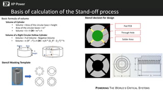
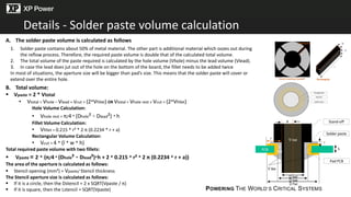
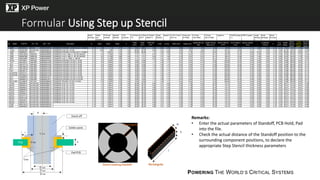
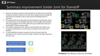
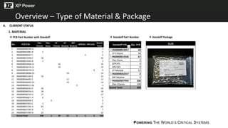
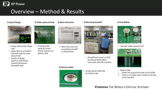
This document provides an overview of standoff improvement for engineering in 2023. It discusses the current status of standoff part numbers and PCBs using standoffs. Various standoff soldering methods are analyzed, including their advantages and disadvantages. Formulas for calculating solder paste volume are detailed. Key metrics for stencil printing like area ratio and transfer efficiency are explained. Guidelines for stepping stencil design are provided. Finally, an example calculation of standoff soldering parameters is shown.


![POWERING THE WORLD’S CRITICAL SYSTEMS
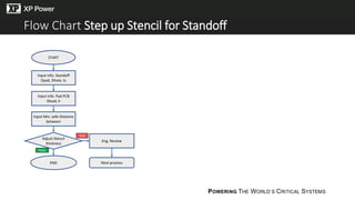
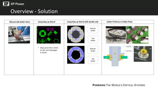
Stepping Stencil
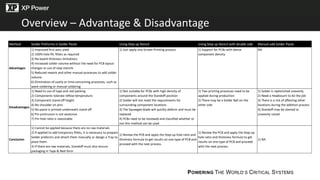
Stepping is critical in many processes, especially when stencil design calculations are being performed based on aperture volumes and area
ratios
Keys to a successful print process
• As a general design guide K1should be 0.9mm[35.4mil] for every
0.025mm[0.98mil] of step-down thickness.
• K1 is distance form the step edge to the nearest aperture in
stepped down area
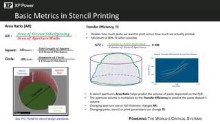
IPC 7525 stencil guidelines
Step Depth K1 Distance
0.010mm, 0.4mil 0.36mm, 14mil
0.025mm, 1mil 0.90mm, 35 mil
0.030mm, 1.2mil 1.08mm, 42mil
0.050mm, 2mil 1.80mm, 71mil
0.080mm, 3 mil 2.88mm, 113mil
0.100mm, 4mil 3.60mm, 142mil
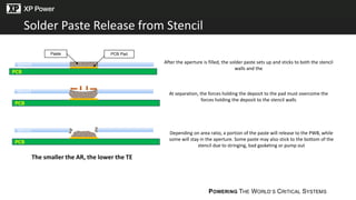
Step Design Guidelines
K1
Step
Depth: no more than 2mil per step
Will lose fill pressure on solder paste
Keepout zone: distance from aperture to edge of step
Minimum recommended: 25mil
Preferred: as much as possible
Larger keepout zones:
Enable better squeegee deflection into recess
Keep the dried paste buildup in the corner of the pocket, away from the
apertures
SQUEEGEE
Keep out
perimeter
25mils
(0.625mm)
2mil, Max per step
Paste Buildup
PCB Layout Drives Stencil Print Process](https://image.slidesharecdn.com/y2023-standoffimpovementv1-240213032948-dcba68ca/85/Y2023-Standoff-Impovement-V1-2-pdf-8-320.jpg)