

Recommended
More Related Content
What's hot
What's hot (20)
Similar to Analysis sequential circuits
Similar to Analysis sequential circuits (20)
Recently uploaded
Recently uploaded (20)
Analysis sequential circuits
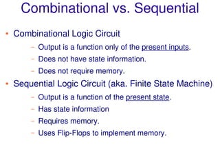
- 1. Spring 2011 ECE 331 - Digital System Design 2 Combinational vs. Sequential ● Combinational Logic Circuit – Output is a function only of the present inputs. – Does not have state information. – Does not require memory. ● Sequential Logic Circuit (aka. Finite State Machine) – Output is a function of the present state. – Has state information – Requires memory. – Uses Flip-Flops to implement memory.
- 2. Spring 2011 ECE 331 - Digital System Design 3 Synchronous vs. Asynchronous ● Synchronous Sequential Logic Circuit – Clocked – All Flip-Flops use the same clock and change state on the same triggering edge. ● Asynchronous Sequential Logic Circuit – No clock – Can change state at any instance in time. – Faster but more complex than synchronous sequential circuits.
- 3. Spring 2011 ECE 331 - Digital System Design 4 Sequential Circuits: General Model ● Memory – Stores state information – Realized using Flip-Flops ● Combinational Logic – Implements Flip-Flop input functions and output functions – Realized using logic gates, a ROM or a PLA
- 4. Spring 2011 ECE 331 - Digital System Design 5 Sequential Circuits: Models ● Moore Machine – Outputs are a function of the present state. – Outputs are independent of the inputs. – State diagram includes an output value for each state. ● Mealy Machine – Outputs are a function of the present state and the present input. – State diagram includes an input and output value for each transition (between states).
- 5. Spring 2011 ECE 331 - Digital System Design 6 Sequential Circuits: Models
- 6. Spring 2011 ECE 331 - Digital System Design 7 Sequential Circuits: Mealy Model output Present state Next state
- 7. Spring 2011 ECE 331 - Digital System Design 8 Sequential Circuits: Moore Model Present state output Next state
- 8. Spring 2011 ECE 331 - Digital System Design 9 Sequential Circuits: State Diagram State Output Input Moore Machine Each node in the graph represents a state in the sequential circuit.
- 9. Spring 2011 ECE 331 - Digital System Design 10 Sequential Circuits: State Diagram Mealy Machine Each node in the graph represents a state in the sequential circuit. Input State Output
- 10. Spring 2011 ECE 331 - Digital System Design 11 Sequential Circuit Analysis
- 11. Spring 2011 ECE 331 - Digital System Design 12 Analysis: Signal Tracing 1.Assume an initial state for the sequential circuit. All Flip-Flops reset to 0 (unless otherwise stated). 2.Determine the sequential circuit output and the flip- flop inputs for the first input value in the sequence. 3.Determine the next state of each Flip-Flop After the next active clock edge. 4.Determine the sequential circuit output and the flip- flop inputs for the next value in the sequence. 5.Repeat steps 3 & 4.
- 12. Spring 2011 ECE 331 - Digital System Design 13 Example: Moore Machine input Flip-Flop inputs output State = AB
- 13. Spring 2011 ECE 331 - Digital System Design 14 Example: Moore Machine 0 1 1 0 1
- 14. Spring 2011 ECE 331 - Digital System Design 15 Example: Mealy Machine
- 15. Spring 2011 ECE 331 - Digital System Design 16 Example: Mealy Machine
- 16. Spring 2011 ECE 331 - Digital System Design 17 Analysis: State Tables and Graphs Although constructing timing charts is satisfactory for small circuits and short input sequences, the construction of state tables and graphs provides a more systematic approach which is useful for the analysis of larger circuits and which leads to a general synthesis procedure for sequential circuits. The state table specifies the next state and output of a sequential circuit in terms of its present state and input.
- 17. Spring 2011 ECE 331 - Digital System Design 18 Analysis Procedure 1. Determine the Flip-Flop input equations 2. Determine the Sequential Circuit output equations 3. Derive the Next State equation for each Flip-Flop Using the corresponding input equation And the Flip-Flop characteristic equation 4. Plot the Next State K-map for each Flip-Flop 5. Construct the State Table (aka. Transition Table) Assign a state label to each binary state assignment 6. Draw the corresponding state diagram (aka. state graph)
- 18. Spring 2011 ECE 331 - Digital System Design 19 Example: Analyze a sequential circuit using D Flip-Flops
- 19. Spring 2011 ECE 331 - Digital System Design 20 Example: Analysis (D FF) Derive the State Table for the following Sequential Logic Circuit:
- 20. Spring 2011 ECE 331 - Digital System Design 21 Example: Analysis (D FF) The flip-flop input equations are: DA = X xor B' DB = X or A Z = A xor B The next-state equations for the flip-flops are: A+ = DA = X xor B' B+ = DB = X or A The sequential circuit output equation is:
- 21. Spring 2011 ECE 331 - Digital System Design 22 Example: Analysis (D FF) The corresponding next-state (K-) maps are:
- 22. Spring 2011 ECE 331 - Digital System Design 23 Example: Analysis (D FF) The state table, or transition table, is then: A+ B+ A B X = 0 X = 1 Z 0 0 1 0 0 1 0 0 1 0 0 1 1 1 1 1 0 1 1 1 0 1 0 1 1 0 1 1 Present Next State State X = 0 X = 1 Output S0 S3 S1 0 S1 S0 S2 1 S2 S1 S2 0 S3 S2 S1 1
- 23. Spring 2011 ECE 331 - Digital System Design 24 Example: Analysis (D FF) The state diagram can then be drawn from the state table:
- 24. Spring 2011 ECE 331 - Digital System Design 25 Example: Analyze a sequential circuit using JK Flip-Flops
- 25. Spring 2011 ECE 331 - Digital System Design 26 Example: Analysis (JK FF) Derive the State Table for the following Sequential Logic Circuit:
- 26. Spring 2011 ECE 331 - Digital System Design 27 Example: Analysis (JK FF) The flip-flop input equations are: The next-state equations for the flip-flops are: The sequential circuit output equation is: JA = X.B JB = X KA = X KB = X.A Z = X.B' + X.A + X'.A'.B A+ = JA.A' + KA'.A B+ = JB.B' + KB'.B A+ = X.B.A' + X.A B+ = X.B' + X.A.B
- 27. Spring 2011 ECE 331 - Digital System Design 28 Example: Analysis (JK FF) The corresponding next-state (K-) maps are
- 28. Spring 2011 ECE 331 - Digital System Design 29 Example: Analysis (JK FF) The state table, and transition table, is then:
- 29. Spring 2011 ECE 331 - Digital System Design 30 Example: Analysis (JK FF) The state diagram can then be drawn from the state table:
- 30. Spring 2011 ECE 331 - Digital System Design 31 Example: Analyze a serial adder
- 31. Spring 2011 ECE 331 - Digital System Design 32 Example: Serial Adder The serial adder adds two n-bit binary numbers. (serial) inputs (serial) output present state next state
- 32. Spring 2011 ECE 331 - Digital System Design 33 Example: Serial Adder Truth Table for the Full Adder:
- 33. Spring 2011 ECE 331 - Digital System Design 34 Example: Serial Adder The state table, or transition table, is then: Ci+1 Sum Ci XY = 00 XY = 01 XY = 10 XY = 11 XY = 00 XY = 01 XY = 10 XY = 11 0 0 0 0 1 0 1 1 0 1 0 1 1 1 1 0 0 1 Present Next State Output State XY = 00 XY = 01 XY = 10 XY = 11 XY = 00 XY = 01 XY = 10 XY = 11 S0 S0 S0 S0 S1 0 1 1 0 S1 S0 S1 S1 S1 1 0 0 1
- 34. Spring 2011 ECE 331 - Digital System Design 35 Example: Serial Adder State Graph for the Serial Adder: What type of state machine is this?
- 35. Spring 2011 ECE 331 - Digital System Design 36 Example: Serial Adder Timing Diagram for the Serial Adder:
- 36. Spring 2011 ECE 331 - Digital System Design 37 Example: Analyze a state machine with multiple inputs.
- 37. Spring 2011 ECE 331 - Digital System Design 38 Example: Multiple Inputs State Table for a state machine with multiple inputs:
- 38. Spring 2011 ECE 331 - Digital System Design 39 Example: Multiple Inputs State Graph for a state machine with multiple inputs: How many paths leave each state? What type of state machine is this?
- 39. Spring 2011 ECE 331 - Digital System Design 40 Questions?