1. 'I"
5.48 Digital Electronics
14. Tabulate the PLA programmable table for thc four Boolean functions llstcd
below.
A(x,y, z) ~IIIl(O, 1.2,4,6)
B(x,y,z) ~ L>"(0.2.6, 7)
C(x,y,z) ~ LIII(3.6)
D(x,y,z) ~ L"I( 1.3.5.7)
15. Tabulalc lht" PLA programming table for the four Boolean funcliom listed
below. l'1inillliz,e the number of product terms.
A(x,y,Z) ~ L(1.2.4.6)
B(x,J',z)~ L(O, 1,6,7)
C(x,J',z) ~ L(2,6)
D(x,y,z) ~ L(l,2,3,5, 7)
16. Derive the PLA programming table for the combinational circuit that squares
a 3-bit number. Minimize the number of product terms.
17. List the PLA programming table for thc BCD to excess 3 code converter
whose Boolean functions are simplified.
•..1
18. List the PAL programming table for the BCD to excess 3 code converter
(,) whose Boolean functions are simplined.
19. The following is a truth table of a 3-input, 4-outP111 combinational circuit.
,I .
Tabulate the PAL programming table for the circuil and mark the fuse map
,.
,~·.I ill a PAL diagram.
Inputs Outputs
x y z A n C D
0 0 0 0 1 0 0
0 0 I 1 1 1 I
0 I 0 I 0 I 1
0 I 1 0 1 0 I
I 0 0 I 0 1 a
1 0 I 0100 1
1 1 0 1 1 I 0
1 1
-
I Oil, I""~
Chapter 6
Synchronous Sequential
logic Circuit
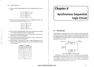
6.1 Introduction
A block diagram of a sequential circuit is shown in Fig.6.1. It consists ~f a combi
national circuit to which storage elements arc connected to form a feedback path.
The storage elements are devices capable of storing binary information. This bi
nary information stored in these elemcnts at <IllY given time define the state of the
sequential circuit attltm time.
Inputs
" " ' - - - I
.r-::-:-
.-----, Outp t
Feedback
path
Fig 6.1
com~lnalional I us
CirCUli I
The sequential circuit receives the binary information from external inputs.
These inputs and the present state of memory clements determine the binary value
of the outputs of the circuit. They also de~I"Illillc the condilion for changing Ihe
state in memory clelllems. Thus. the m:xl state ll" l!l(' memory clements is also a
function of the external inpuls and the prCSl.'nl Sl.ltL'.
Block diagram of sequential circuits
www.Jntufastupdates.com 1
2. !'i'
~i
"
!.:
,.
,"
,
'
'.,
') ,
,
'":
'J "
;~) ': I
I':' ,
.,~ )
"
6.2 Digital Electronics
6.1.1 Mealy Model Sequential Circuit
Fig 6.2 shows the clocked synchronou.s sequential Mealy machine. The output
of mealy n1<lchine is [he function of present inputs and present state (Flip flop
outputs). If X is input. Qil is the present Slate and the next state is Q(n+ I). rhe
output of Mealy funclion (Zl i~ given below.
'. . ';'~. -
Synchronous Sequential Logic Circuit 6.3
Z = !(Q,,)
The difference~ hetween the Moore machine and Mealy machine fire tabulated flS
follows
S.No.
J.
2.
3.
Moore machine ~
The output or this machine' lS
the func(ion of the present slatc
only.
Input changes do not affecl lhc
oUlput
It requires more number of states
for implementing same function
~ Mealy machine
I'lts output is funclion of presel!,l
input as well as present state...
!IlPU~ changes lIlay ~f[cet the
OutpUl of the circuit
It requires less nLlmber of stales
ror implementing same function
Next ~tal"
N~Xl Stal~
ln~ul X
Qn+1
r-;=:
Decodor
Comblnal1onal
logic clrcult
Fig 6.2
·Z~/(X.Q,,)
Momory
L-j
Output
l
r___~,"5"nl Slale
Ourpul
Oecodor
Q" Caml>ln.Uan.1
IOQlc cirCUli
Mealy model sequential circuit
6.2 Analysis and Synthesis of Synchronous Sequen
tial Circuits
SyntheSis
Analysis
Procedure
Procedure
The output of memory element is conneeted to the input ofoutput deeoder nnd
next st<He decoder circuit The output of memory element is considered as present
state.
6.1.2 Moore Model Sequential CircUit
NOXl Sl.1te
Oc<;odcr
lputX
,-' .i .~'~ Momory
r
..,'
Output
CombInational Qn4',
r;::::: l
logic circuit
NUl Slate ~resenls.tale
OUlput
Cecoder
Cambrn.tlan.1
lOOk: cTrcult
L--Ij
.;
Fig 6.3 Moore model sequential cIrcuit
Fig.6.3 shows (he block diagram of J Moore machine. The output of Moore
machine depends only On the present state. So the output of Moore m,lchine is <1
function of its pres~llt stare (QII). If the input i.' X. the next stale is Q(n+ I) and the
p....:sent state is QII' The outpHt of Moore m.achille is represenced mathematically
by
Fig 6.4 Flow chart
www.Jntufastupdates.com 2
3. - -
6.4 Digiw! EkrlmlliL'.<;
The behaviour or sequential circuit C~lll be determined from the inputs, Dulpllls
and slateo[ its nip nop~. The outputs and next state ure botha function nfits inputs
and the present stale. The analysi1i of a sequential circuit consists of obtailllng a
stale table or stOlle lliagram fm the time sequencc of inputs, outputs and internal
states. The nnaly:>i:- 01' the cloc~.d segllential circuits can be done by following
the procedure as shown in Fig.6.i:-·'The reverse process of analysis is known as
synthesis of clocked sequential logic circuit.
POl' the analysi" or sec!uenlial circuit, we staft with the logic diagram. The
excitation equatioll or Boolcnn expression o!" each flip-flop is derived from this
logic diagram Then. ((l ohlain Ihe next state cCJui1tion, we insert lhe cs.citation
eqLtations into lhe characterisfic Cc]lliltiollS. Th~ output equations can be derived
from the schematiC We can generate thc slate table lIsing output and next stale
equations.
6.2.1 Analysis of Example Sequential Logic Circuit
Js Oil
®
KB as
I ,11
I'" _.
s
/'
B
JA
x
®
B
K,
~ IV I IJ
= ,
'fi
Fig 6.5 E~ample or sequential logic circuit
Fig, 6.5 ~hows a clocked scqu~iltial circuit. It Iln~ one input variable x, one
output variable y and two clm:ked JK flip flops. The /lip flops arc labelled as A.
and B and their outputs arc labelled as A and A. Band Brespectively.
Step 1 : Type of circuit
The output0') of gi'cn logic circuit (Fig.a.S) depends on present inpllt and
also on present state (Flip /lop outputs) of flip flnps, so that lhe given sequential
logi(,; circuit is Mealy sequential machine.
Step 2 : Excitation eqUlltions
The excitation cqU<lllUm or Boolean expressinns of /lip Oops A and R arc
oblained. The equation:'. will be in thc fonn or prCsLllt slatc.~ A and Band e:-.h'rnal
SynchCOlJOUS ScqtJellliiJ1 Lo,yic Circujl 6.5
inpOlX, since here are tWO 1K flip flops whleh have outpU' A and IJ. Therefore the
ex.citation eqli.llioll (equation formed for njp flop input)
Fol' Flip nop .. A 1/ = xB r'
KA ~xB ~
For fill' ftop - B 1/1 = xA
K,,=xA /
St l,3 : Next stale equatlun. T.he slalC equations ean be det'iced ,hre"'y from
e
the logic diag ,,,". Looking-" Fig.65 we can see thai thc si~lal fur J Inpul of
r
Ihe flIp 110p A IS generated by the funclion Ii" and Ihe signal for input K by the
funello Bx. Snbslilu'lug J = Ii" :lnd K=B:i IIlto a JK llip 110p cl",,'acreristie
n
equation g'['cn by
Q!I+1 = fQn+KQIl
State equatlon fur nlp flop A
:JT~ -Il
where QII =A J
AMI == (lb:)Q!1 + (Bx)Q"
=BxA -'- B.'A
~ ABx +A(B-')
=ARx+A(8+ x)
=ABx+AB+A.>'
=AB+x(A+Alf)
(A +AR = A+8)
=AB+x(A+B)
A/I-r! == AB+Ax+lh
State equalion for flip nop B
Similarly, we can rmd lhe stale equation for llip 1101' R J =Ax and K ~Ax.
Therefore the ~lutc equation of flip fillp B is given as
B,,+{ =Ax B+ (A x)1l
=AxS +(A +x)B
= AxB+AB+ m
=x(AR +B) -1- AH
~ 'CIA + B) +AB
Nil, =.- xI 13 x ).-8
www.Jntufastupdates.com 3
4. 67
6.6 DigitHI Electl'On~c(j
Output equation
The give~ sequential circuit has output y. The output equation can be found from
the Fig.6.S which is derived using three input AND gnlC
fr~ABxl
Step 4: State table
Table 6. is the :-itate tuble for the givcn scqllcliLiallogic circui!. It represents
the relationship belween inplt, outpUl alld nip nop stales. It consisls of Ihree
column:-;: preSClll slate, nc.xI state and OUlput
Present state: It specifies the stale of lhc llip flop before occurl'cnce of a
clock pulse.
Next state: It is the state of flip flop after the application of a clock pulse.
Output: This section gives the value of the OUlput variables uuring the
.,' present state. Both next state and output section have two columns repre
, senting two possible input conditions x = 0 and x = I.
, ,
,
..,
., Table 6.1
; (.
,
': .
".
"
~
Output
Present state Next slate
All AB y
AB x-O x-I x-Olx-I
00 00 10 0 I 0
01 01 00 0 0
10 11 10 0 I
1 01 II 0 1
We ean derive the state table as follows
(il If present state AB ~ OO,x ~ 0
Vhen a present state is 00 Le. A= 0 and B =0 and input x = O. the next
slate is obtained by using next state equation
Nexl slate for Hip liop A
A,,+l =AB+Ax+Bx
~ 01 +00+ 1.0
~O
Synchronous Sequential Logic Circuit
Next stale for Hip Hop B
811
+1 =A'-+-Bi+AB
~0.1+0.1 +0.0
~O
INext "ate for this e~,e AI! ~ DO!
(ii) II' presenl Slale AB ~ OO.X ~ I
Next ,tale for nip·nop A
Alll
L =Al3+Ax+Bx
=0. +01 + l.l
~I
Next state nip Hop B
811
+1 =AI+Bx+AB
~O.O+O.O+O.O
~O
Next state for this case AB ~ to I
Similarly we can obw.in next state for aU these different cases as shown in
the table.
(iii) Determine the entrie:; in the output section. For this, we have to examine
AND gale fOf all possible present sUlte5. and inpul.
(al If a present slate AB ~ 00.
oulput y ~ ABx
~O.IO
ly~OI
If a present state AB = 00.
(bl
Ol1PIl Y= ABx
~O.ll
I'~ 01
X~O
x=l
www.Jntufastupdates.com 4
5. 69
6,8 DJ'gilai Electronics
Thus, the state table of any sequential circuil can be obtained by the same pro~
cedure used in the above example, This example cant<lios 2 flip naps and one
input, and one outpUl, producing four rows, two columns in lhe nex.t stale and
output sections. In general, a sequential circuit with m flip~Hops and Il~inptlt vari~
ables produces 21/1 rows <lnd one for ~ach stelle and 2/1
columns, one for each input
combination in the next slate and output sections of the stale table.
Step 5 State diagram
Stale diagram is a graphical represclll<lion of a state table. Fig.6.6 ~hows the
slate diagram for sequential circuit. Here e(]t.:h state is represenled by <l cin.:lc.
and Inlllsition beLween Mates is indicated by directed lines connecling the circ!e~.
Thc binary IlLII1lber inside each circle i.dcnilics the state reprc.-,;clHL'd by the circle.
The directed lines are labelled with lwo binary numbers separatcu by ,I .symbol '/'
(sla~h). The inpuL valuc that causes the stale transition is labelled first and output
value is next
010
00
/~;
0100' '01)1/'
~/~
11
110
Fig 6.6 State diagram of Fig.6.S
Example 6.1 Derive the state table and stale diagram for the sequcntial circuit
shown in Fig.6.7(a).
[J Solution
Step 1: Type of circuit
The output y of given sequential circuit (Fig.6.7) depends on the pr~Oenl input
and also present state (flip flop output) of flip Oops, so the given sequenti<lllogic
circuit is Mealy sequential machine.
Step 2: Excitation equation
For flip tlop A
J, = I' + R
1( = A
Synchronous Sequential Logic CirclIil
B
x---.-------L:/
CP ----rl> (0 ®
""rd' "
Ii.
_ K Q I---',.--. a
-rl"A 0A B B B
y
Fig 6.7
For nip nap B
JR = A +x
KR = B
Step 3
We know thal characteristic equation of JK flip flop
Qn+/:::: f?ln +KQII
State equation for flir flop A
(where Q" = A for tlip nop A)
A'ITI :::: tx + B)eL + AQn
= (x+B)A+AA
=Ax+AB+()
AII.II ::::Ax+AB
State equation for flip nap B
(vhere QJ1 = B for flip tlop B)
all, ::::: (A +X)QII + liQII
= (A H)B +BR
BIIII ::::AB+H.-,,:
OutpU[ cqlalion
' __ ::Bx
www.Jntufastupdates.com 5
6. , I.,
~..
i'
"
6.10 Digital Elcc}.1"On;cs
Step 4 : Stale lable
IPre"en) "talc Ne~:l',!(' Output J
ccc----t-_A_D-oc-+i AD y
~-*~ri--I~~ x~~
f---iQ- 0 I r UII-l 0 0 --1
L__ 11 --~- - __ '-____ __ I
1----- - ()O_ ; IJO l-.Jl.--L.QJ
Step 5 : Statr diagram
Fig 6.8
•
Example 6.2
Derive the state table <lnd stale diagram (01- the sequential circuit
shown in Fig 6.9
o SOlution
Step 1 : lypc of circuit
The oUlput of a given circuit(See Fig.69) depends on prescnt input and <IIso on
pl:esenr states. so the given sequential logic circuit is Mealy nwchines
Step 2: Excitation Equatiun
For flip nap Ii
/J.[ = A.r +B.I'
For Flip Hip B
DII ::-.-Ax
For Output
Y=AB+x
Synchronous Sequentj;jJ Logic Circuit 6.11
Step 3:
We know that cbaracteristic equation of D flip flop (next state depends on input
D)
AJJ+1 =DA
[A,,+I =Ax+8xl
BIH-] = Dn
!B"cl=Ax!
A
, 1 '--- I
"
DA QA
A
B -----L.-/
I I ®
A
I A:~y
Q
B
~
®
0, B
I
CP
Fig 6.9
Step 4: State lable
The state [able contains four rows and three columns. The next state and output
have two sub columns.
Output
I PI"esent state I Next stale
AB
I AB Y
x-I
x-O
AB L.=:-O .1'=1
0
01 00
00 I 00 I OJ
I
I J
I
10 DO I
10
1- __ I
10 I
II I DO
0
0
0
o i
www.Jntufastupdates.com 6
7. 6./2 Digiwl Electrol1ic"
Step 5: State Diagram
010
0/1 ~
..A.
011
:$
=----> 11
110
~~O
10
b
110
Example 6.3 •
Derive the Slate table <llld slale diagram for sequellli'll circuit
shown in Fig.6.lD
.,
B
I ~A
®
Qtl xrl:'®
Q,
i
,
A
xJ ~ K QA,:O: 1x --/u---+--1.2 G,
B
'" j •'::::::[)--.,
Fig 6.10
o Solution
Slep 1 : lYpe of circuit
The output y of the sequential eireuil depends Oil present state only. so the given
logic circuit is the Moore type circuit.
Step 2: Excitation equ~tions
For flip Oop A
JA ~ S
KA ~ SI
For Dip Oop /i
JB ~ I
K!I~A,Bx
."=Aq~n
Synchronous Sequential L(l~ic Circuil 6.13
Step 3 :
V>/e kno' thaI chanlcteristics equ:llion of JK flip ~op
A1l1-1 =iQ'I+KQII
State equation for flip flup A :A". t ~ SA +(BX) A 1,- Q,,~A)
~BA +A(B+.r)
~ SA +AB+x
A,.. t ~ (A ED B) +.r
Stale equation for nip flop /i : Ii" I =.rB+(A fBx)/i
=xB+(Ax+/lx)ll
Ii" "' =is+AxB +Ax'/l
Step 4: State table
Present state lIied state Outpu
x-a x-I
-
y
AB AB AB
00 01 00 0
01 II 10 -
I
10 II 10
.
I
II 00 11 0
-
q
'
-J
State diagram
~Slate
o Input
",",0
0/
1/0
~
0
CD,!
0
..-.--- ------.-----.---- '1
- - - - - - ~ -
INoll': The state diagnllll for lvloor~ 1l1arhine is dilTel'cJl frnlll r-,.'kaly 1l1i.l'hinc.
IHel-(, (,liCit circle is coded wiLh qaL..: binary number/outpul. !
L_________ _ . .
ill
www.Jntufastupdates.com 7
8. ~,'1
':~.
;,
f.' "
I"
"
.'
j'
('
;.;
'
t.
6.14 Digical EJectronits
6.3 State Reduction
Any logic design process must consider the problem of ll1in1mizing the cost of the
final circuit. One way to reduce the cost is by reducing the number of nip nops. i. e.
by reducing the ntlmber of states. The state reduction technique basic;llly ..}Voids
the introduclion of redundant equivalent states. The reduction of redundanl .'Hates
reduces the number of nip flops and logic gates required,·tbus redudng Ihe cost of
the lina! circuil. T,,'o stales ..we said'to be redundant Or ~qllivalenl. irevery possible
set of inputs gcncralL'eXilClly the same outputs and Ih~ saDIe neXl S!<lte.". Whcn LwO
states arc equj'alem. une of thelll can he removed VilIIDll{ allefing inpuL-oUlput
relationshIp. Le{ ll .... consider the state diagram -"hown in Fig 6.11. The S[;J1C.", arc
denoted by lcllcr ,,-vmbols instead of their binary yallles because in ~ta[e reduction
technique internal S[,ltes are <llso important bUl inpul omptlt sequences are more
lmportant. The procedure conrains two steps.
110
0/0 010 010
Fig 6.11
Step 1: Finding Ihe slale lable for lhe given slale diagram
First the given slale diagram is converted into a Slale table, Fig.6.11 sbows the
example of state diagram.
Output
Present state Next state
x=1 x-I
x-o x-O
c
a 0 0
b Both are
d • equiva;enL slates
b _" .1... _ 0
:c····· -.
:_T"
D
because of state
_
::Ll::X: --~---
d----- c and e having
a d
.. -. -.-. "-.-" - - ._._" . 0
same nex! slate
'.e, _. _. _. _" _. c:. _. _" .. .d. _• ..~ .. - ""."!
0
-', and same output
Slep 2: Finding equh'alcnl slales
The two present stale.... go to the same next sJ,lle ,md llave th~ sallle outpUI for
both rhe input combinalions. We can e,lsily find Ihis from tile strite table. ....Wlc.~
6.15
Synchronous Sequential Logic Circuit
c and e are equivalent. This is because bLlth c ami e states go to .<tates c and d
oulputs of 0 and I for. = 0, X = 1 respectively. Therefore, the stale e can be
removed and replaced by c. Tbe flOal reducod table and state diagram are given
ut
in tbe table 6.2 and Fig.6.12. T~e second row 1al'e e state for the ior x = I. it
replaced by c beci.lse tile states c and e an: equivalent.
Table 6.2 Reduced state table
1/0
l)resent
state
AB
-...,.--- ,
Next ~ I
II
010
h-;l
AB . . 1/0 _ --------l/I-{ c ) )010
oLI
x= W '"
x=O
r=()·r=l
. , I '
0
0
I) I c
a I 0 /1/1
1
d c
b )
]
'"
0
c d
c 0
0
a d
d
1/0
Fig. 6.12 Reduced state diagram
Obtain the reduced stale table and reduced slare diagram for a
Example 6.4 seql;ential circuit whose slaW diagram is shown in Fig.6.13.
010
111
Fig 6.13
www.Jntufastupdates.com 8
9. 6.16 Digital Electronics
o Solution
The given diagl'tllTI has seven slales, one input and one outpUl. As per the slep J,
lhe given state diagram is conver~ed to a state table.
State table
Table 6.4(a)
Present slate Next state Output
x=O x 1 x-a x-'
a a b a a
b c d 0 a,
c
i a d a Both are
0
•cJ. . .. . .. _. .e• .• equivalent stales
. .f ... .. 9.. __ 1
'•.e•••••.• _. _~ •. because of slale
.f....... .. 9. __
.. .t.. _. ....i:.•
_. .P....
e and 9 having
.. I ... ,.0.... ..1, same next stale
'••9•.•••.••••~ •. .. J.. _... 9.... . !.' •D-and same oulpul
Fl'Om the above state table, it is clear that Slates e (Illd g are equivalent. So the
srate g is replaced by state e. The reduced state table is shown in Ex.6.4
Reduced state Table
Table 6.4(b)
Present state Next state Output
x 0 x I x 0 x I
a a b 0 0
b c d (J
0
c a d (J
0
d
lBOlhare'1-[l l' (J
I I
equivalenl
e a
slales (J
I I
I l' 0
I I
From the above reduced table, Slates d and f are equivalent, hcncc '.I" Gil) be
replaced hy d and it can be removed. Theil lin,tlly the reduced slale lahlc i.., shown
in Table 6.4(c)
Fiu,,, reduced tllble
The- Sl~lli..: diagram of tile reduced slale Tallk is shown in Fig.6.4(l1).
Synchronous Sequelllial Logic Circuit 6.17
0/0
110
Present slate Next state <hll,"'" 1
AB I AB
1/1 010
l ,II!_-~-l-'-c:.'.' "E~
(/ (/ /1 O! 0 I
b
I, ({ d 11 I Il
OlD
, ,
I/O
, II d II I) I
010
d 1L' (/ (I 1
d J' t
L-_ (' ~ _l~ _ _L_J 110
0
1/1
II
6.4 State Assignment
III sequential circuits we know lh,ll the behaviour of the circuit is defined in terms
of its inputs. present state, nex.t sl<ilc and outputs. To gencrate the desired neXl
state at particular pre~ent slale and inputs, it is necessary to have specific flip flop
inputs. These flip flop inputs are described by a set of Boolean functions called
nip (lop input functions. To clclermine the flip flop input functions, it is necessary
to represent stales in the Slatc diagram llsing binary values instead of alphabets.
This procedure is known as S(aLe assignmcnt. Tlle following rules are used in stale
a~signnlent.
Rule 1. Stales having the S;llll~-~~~l st<lles for a given input condition should I
have assignments which can he grouped into logically adj.1cent cells in a
K-map, (Fig.6.IS) , _ . ~
100 111
e (3
100
Fig.6.15 Fig.6.16
r---- , " '" .. -_. ---- --'--,
II{ulc 2. Slales having c1ifl.Oen.:'l1t lk'XI Slaks should h,wL ass.ignlllenl vhich can I
lbi..: grouped into logically ad.i~n'IIII.·~lI.., in K-map. (Fig,().161
. _ .__. . .. - _ . . _ . - - ----_. , ".
www.Jntufastupdates.com 9
10. I
('.18 Digital Eleclronics
Example 6.5 Design a sequential circuit lI~illg D flip flop for ,.1 :-;La[e diagram
given below. Usc state assignment rules for assigning states and
compare the required .c9,rnbinminnal cin:uit with random slale
1/1
0/0
Fig 6,17
, '
[j Solution
l.:
The st,ltes are a,b,c,d <Ind e, Each slate is randomly assigned.
{f ~ 000, b ~ 001, c ~ 010, d ~ 0lJ, e ~ 100. The remaining combinations are
considered as donOt care conditions.
EXcitation table
Present state Input Next State Output
A B , C X Al1 +J B".,., (1/+ J Z
0 0 0 0 0 0 0
0 0 () . 1 () 1 0 0
0 0 I 0 0 0
0 0 J 1 I 1M:
I
o 0 0
()
0 1 0 I o 0 0
0 I 0 I 0 I I ()
0 I I 0 0 0 0 0
j
0 I I J 0 J
, .
0 , 0
I 0 () 0 0 0 I
0 I
I
f-r'+oj- 0, J 0 0 0 0
i
Sym:17rnnous 5'equemial Lagh- Circliit 6.19
i Pr1cscnt state Input ~t State Output
U ' 0 1 0 rX X X X
LI 0 1 J tx I X X -r-
K-map simplification
The LJ nil) lIop inpul is ~qL1a! La l1ex stelte 'lnd Ihe flip nop c.pl::~si(l11 i~ obtained
directly"
Expres_'iion for flip flop inpul DA Expression for flip Flop input Do
.c, .ex
w ", A , uu u, n IU,
A "' '"
, 3 1 : 2
o 0
lJJ
, ,
, •
1
:1:
,12: :
" "
" "
x x
:.~;
, , 11,_, ".
x
D x
!xl
D 0
, 1 ,,
fil ~
" 4
5 : , 7
•
t!i
" 13 15
"
1 x x x x
, 9 11 10
i~':
D x
De=ACX:"SCx
Expression for flip nop inpul Do
.c
ov -. .- A' -- -.
D 0 , , ,
~ ·.~~~i: if::
1 ' ~ "r 7
,
: 1
" 13: :" "
1
x ..~J x X
fs-, 11
D '"
x x
Dc:::A8x + Bex
:
J 0
, , ,
4 , 7
•
1
:"r
"
.'••-, 13 15: : 14
1
x t~J x
x:
• " " 10
,
D ...,.1: ~..
Z=BCx+Ax
The random a~signll1ent reqllires
7 1l11"l:L' illPLl~ AND gates
I two inplil AND gates
4 [,:0 input OR gates
Total 12 gillc" wilh 31 inputs and ~ nip Oops are required [0 COllslru....t the sequen·
ti,1i logic rirL"lliL. N(HV 'e apply slale assignment rules. thell rolln' the abovc
SICps.
www.Jntufastupdates.com 10
11. 6.20 Digital Eleclronics
From Rule I, The slates ~-;~cTdmCJst be ~dj~ceJ1t l
From Rule 2, states band C l11ust be adjacent We Form the adjacent cells in I
I
the 3 variable K-map
00
0
4
01 11 10
2
1
:!J:
3
::C:'
5 7 6
::e:,
:~ :
Excitation tahle
Pres-erlt-st-.llC : il11~ut Next StIlle . - - ':- Ol,tpiit
,4-:-B: -C X AI;I"r--:·ll;I~-I-:-CIlr-;-~-·-i··
-0: 0 ~ --Ii 0 - II --6 -, I - . 0 - ,
C
-6 -:- 0- ~ -6' 16- -,I -:( _c - b" - -:
-6 -:- 0- ~ -F :- -6 T:---6 -: 1- -,
-
-
-
0 ---:
1: :rnr;-{f:::(-i::r::-::r:::
' : ; " 6-:--(~--6-, --j" - -x --'- -x-.,--x--_c - - -x---,
n :6::::C:L:::o:: i:_::1::::".t::-:::0::::
. 0 : I: I I I 0 I 0
t rmnrrur:y
1 : 0: I I 0 0 0 1
-e-(~---6 -,--6 -x--:--x--:--x-- _:c_ -X-
-j-:- -1- ~ --6 .-,---i - 'x' -:--X--:--X- --, .. -X- --
-1-:-('---1--'-6--- -'6--:--0--:-0---':---1
-
F> 1 ~ ---r --,- i -. -6 .---6 --:. 0- --c • 0
-'- - - ~ -- - - - ,
K- Mall simplification
E:o:pression for r.ip foop input DA
Expression for r.ip roop input DB
C
AS' UU 01 11 10 ABC
, 00 01 11 10
1
J 0 3 .2__ • 1
o 0 3 2
: 1 1', 1
7,
5
7 6
o 5 1
1 • x x "! _..1; 1 •
,.
6
13
I 12 15 13 15 14
1- J? .
x x __ ..x: x 1
9 11
,8 10 9
) 8 11 10
x x x :~ ~: :{
DA =AC
°s=ASx+-ABx
Synchronous Sequenlial Logic Circuit 6.~ I
Expression for r.ip f,op Input Dc Expression for [:IP [,ap input DD
,C ,C
UU U1 11 10 AS
1 41 6 i
...~- 1 ;
--....
1 12 13
"
x x
) 0 _..... 3 2
AS
1
{'1" ·"1'..
1
1
5
7
x
1
15
9 11 1O
x
) 8
x
uu u,
" 'u
J 0 1 3 2
1
1 4 5 1 7 6
12 13 15 14
1 ::~.' x :.1
B 9 11
:~ :':
10
D x :~
"-.
Dc=A Do"'IBx+ABx
Under lho..: :-.1~lle assignlll~llt rules, we require
~ three input AND gates
I two input AND gale
2 two input OR gales
A lowl of 7 gates with 18 inputs and 3 nip flops are required to constnlcl the
sequential logic circuit b~lsed on the state assignmeJ1l rulcs.
6.5 Design Procedure
The following steps are followed to design the clocked sequentiallogie circuit.
-- ._----------
l. Obwin the state table from the given drcuit information such as a state
diagram. a timing diagram or deseription.
2. The Ilumber of stales may be reduced by state reduclion technique.
3. Assign binary values to each slate in the stale tnble.
4. Determine the number or flip flops required and assign a lener symbol
10 each Oip Oop.
5. Choose the nip flop type [Q be used according lO the iJpplicmioll.
6. Derivc the excitmion table from the reuuced state table.
7 Derive the expression for flip flop inpuls and outputs lIsing k·lllap sim
plification (Thc presellt stale and inputs ~re considered 1'01' k-Illap sim
p'1.ific~~~?~l)_~_~~. ?_I~~~W l~~~i_~ ~~~~_~l_il__~:')_i_I_I_g;_ l~!P_!~(~P_~_~l.l!~_l_ ~~.t.:~ . _
6.6 Synthesis of Clocked Sequential Logic Circuits
Synthl'sis means lhut, it is [he reverse process of analysing i1 sequemiilllogic cir
cuit. llllhi~ synthesis. we get a logic cir~uit l"rom the infnrllli.tioll Ol'stdlC di~,graill.
-ord description etc. The detailed :-oleps tll.' given in tho..: example. No' we ill
('L' (he dLtailed description (ll" each "(Cp.
www.Jntufastupdates.com 11
12. --
iTI'
,
().~~ Digiwl E/c'I.;IrOnic"
A !'.[ale dii.lgrulll is obtained (rom the vorel description. timlng diagram or
other pcrtincllI information. From tllis stme diagram, we em form a state table.
ThL' reuuction of number of slales and binary valuc assignment to each state
givi::s Ihe r~dLJl:[ion in combinational circuit requiremelll. The !lumber of nip flops
required 10 design ,lilY sequential logic circuit depends on the number of slalcs.
Example 6.6 A sequential circult- has one input <:ll1d one output and its stale
dic.lgratll is shown in Fig.6. JR(.:"l.Dcsi~Jl the sequential circuit
llsing [) /lip nop
010
00
1/0/'1
~"
1/1
;1 010
01 11
" 1/1
i~ :
;';
~ /110
10
~
~
011
~, Fig 6.18(a)
".
o Solution
"
,
, The given ."late diagra1ll consists of four stmes. it hat one tnjJltt (x) and one outpul
(y). The state table for the given stale diagram is shown in Table.6.6(a). It is clear
thal thcre arc no cquivalent stales. Thereforc. lhere is no reduclion in the state
di<:lgran1. As the slale diagram contains 4-slmes. it requires 2 flip-flops which arc
named as A and R.
Table 6.6 (a) - Outpull
- ~lstate ~
C Present slate. ~ x = 0 x = I
:B'=O .'"w I L]
;B AB:~ I
00 . 10 I
( ::_-, " I::~:
Y
:.
'I·· -- -10 fIO-l_ - I [) .J
I
c----- -'I" ,,_ _
-LO~L~_'
L
Synchronous Sequt'IJlial Logic Circuit 6.23
Design using D-f1ip flop
. For the design of circuit using D flip 1101' (or any nip lIop). we need the excitation
laDle. Table Ex 6.6(b) shows the c;.cltation lablc or LJ flip [lop from which we can
develop cxcitalion table [or the required circuil <IS shown in table 6.6(c).
Table 6.6 (b) Excitation table for D-flip flop
r
"",,","""1"'" "'''1'''''","'""'''ll
Q" I Q,,+I ~ !)
-~- [--~--1 I: -·l
1 : Ll_l_~_ _J
l:......I..IUtLIUII ~(1 ......
bl
Inptlt
0
0 0
0 0 I
0 I 0
0 I I
I 0 0
I 0 I
1 I 0
I I
Next state
0 0 0
0 1 0
I 1 I
0 0 0
0 I 0
I 0 I
0 0 0
0 I 0
Output
Flip "up input
~esentslate
x
A B A B DA Da J'
0 0
I I
I 0
0 0
I I
0 0 i
0 I
1 0
- I !
The flip-flop input funclion and the circuit oulPUl function are obtained by
using K-map simplification.
Input equlItion (or) funclion for nip flop A(!).,)
'.B,
A'.~~~l<'O'.
01 1._!J I !..!.:
C~~)
S 17 16
4
C.!';
DA = A)j x +,I B.' +MiX -i-,/lx
~A()jx+B:i)+A(i!'yAIhl
Lelu" consider::: = ax +H~o thenS x+ Bx =~. Simplir) the above equOlion
DA =;h.+A;-:
=A., ,
www.Jntufastupdates.com 12
13. TOp I'
6.24 Digilnl ElccrfOlljc,."
SubstitUlC':: = Yi.r+ III ~ jJ'l x in the above equation
@A ~A"!lBEIlxl
Input equation for nip llop B(Do) OutpLH funclion y
Bx
uu u, w
, "
0 J
~"j
U ..·
• ~--1-:
, ,
I
'.....
A 00 01 11 10
o 0 1Ci~) J 2
CT1
1 • L1 5 7 G ;-1·
. ..... ....
f)u:-::;/f'·:·.-kr y=.':'+AiJx
TilL' input equatiOiI (or nip and outpul equation an~ simulated as follo's
DA =AEDIiElix
DB~Am+ABx
)'=Ax+ABx
:1 ' A sequential circuii using D flip nap is obtained by llsing the above eqmHions as
l:~ / shoWIl in fig 6.18(b).
,
II~' !
"
f; A
B
:}
'V
x--+-!/ /
,
", o,w:---LJ
';. '
o ~
i, ' x
I!~
_ A '
'., CP
°A
,"
Fig 6.1B(b)
6.7 Sequence Generator
olB
D, ,
®
_I B
0,
y
A sequclllial circuil which gcnerates a prescribed sequence of bits, synchronous
with the clock. is referred to as a ~equel1ce generator. We can construct sequence
gener<llors by lwo ways
I. Sequence gcnerators llsing counters
, Sequence gl:llermors using shin rcgisLers
Synchronous SL't/ut:llllaJ Logic Circuit 6.25
6.7.1 Sequence Generator using Counters
Flg.6.19 shows the block diagram of ~ sequence g.1,'CrmtH' u:'ilng counters, It con
tains two stages
1. counter, and
2. next state decoder.
[
L-...o
FF inputs:
[
Design Procedure
E;l
BJ
I
'1:1
Nexr
Slate
~
.
de(Xlder
[S] r-- I
Counter FF outputs
I
Fig 6,19
Step 1 ~ Determine the number of nip-flops required
The number of nip-llops required to generate a panicular sequence can
be determined us follows.
(a) Find the Ilumber of 1's in the sequence.
(b) Find the number oro's in the sequence.
(c) Take the muximurn value from both.
or f1ip~nops, choose Ininimulll value o
If
r 'n'
n is the required tlmnber
to satisfy the following
condition,
muxiO's. ':-):::.: 2"- 1
Step 2: Stale assignmenl
Once the number or Ilip·nops is deci(lctl. we have to assign unique stall~s
corresponding to each bit in lhe given sequence such [hat the Ilip-l1op
representing least signilicant bit gencl'atl'S Lhe given sequence (Lile oUl
put of the flip· nap which represents lhL lei.sL significant bit is lIs~d ttl
represent the given scquence)
Step J: Draw the slale diagram rrom lhe above !'>tatc assignment and obl.lin Ihe
excitation table from the swte lliagnu:l.
Step 4 : Fino Ilc Boolean ~Kpressiotl forcadl lllp-llllj1 l11[1U by U:'iing k:illap and
dri.l' the logic diagram .1'01' l~i: !50nlci.l1l c:-'P'L·s.~iojl
www.Jntufastupdates.com 13
14. II'
, '
;. ,.
6.~() Di.~jl:,1 eleclronics
---~~,-
Example 6.7 Find the number of flip~flops required to generate the sequence
10110110,
,J Solution
III the given sequence, the I1Ulllber of D's are 3 am] Illlllber or l's are 5.
max (3,5) ~ 2"-- 1
5 :; 1'1- I
[/I = 41
II
~..",.....~
Example 6.8 Design a sequence generator using J K !lip-nap lo generate the
sequence 1101011,
o Solution
Step I: Number of flip-flops required
Number of D's in the sequence = 2
Number of 1's in the sequence = 5
Hence max (2,5) :s 2,,-1
5 .5 2'1-1
In =4 i
We need four nip~flops l1<l1ned as A, B, C and D. The desired sequence
is generated by [he D flip-flops output
Step 2: State assignment
I Decimal
equivalent
A B C D
1
:,
0
5
2
7
9
0
0
0
0
0
()
I
0
0
0
I
0
I
0
0
1
0
0
1
I
0
: f,
: 1 :
: 0:
, ,
, ,
: I:
: 0:
:I:
, ,
:,.1:
'---.
Given sequence,
first enter
this column
-~
Assign binary value based
on non-repeated states
Synchrol1ous Sequentiill Logic Circuit 6.27
Step 3: State diagram
Excit:Hion table
Prcscnl state -Ne~( ""llie I
...
Flip-IIup illIJuls I
QA
0
Q8
0
Qe
0
QD
0
Q,
0
QII
I
Qc
0
(l[J
I
I"
0
K,
X
III
I
K8
X
Ie
X
Ke
1
ID
1
f:f)
X
0 0 0 1 0 0 1 I 0 X 0 X I X X a
a 0 I a a I I I a X 1 X X a 1 X
a a I I a a a a a X a X X 1 X 1
a 1 0 a X X X X X X X X X X X X
a 1 a 1 a 0 I a a X X 1 1 X X 1
a 1 1 a X X X X X X X X X X X X
a 1 I 1 I 0 o I 1 I X X I X 1 X 0
1 a 0 a X x x ' X X X X X X X X X
1 a 0 I a a 0 I X 1 a x a x x a
I a 1 a x x x x x x X x x x x X
1 0 I I X X X X X X X X X X X X
I I a a x x I x x x x X x x x x X
1 I a 1 x X x x x X XI X IX x x X
I I I a x x x x x x XI XI x X x X
I 1 I I X X X X X x XI Xl X X X X
I Note: The unused slales 4, (I, 8. 10, I I, 12, 13, 14, and 15 arc considered as X
K-map simplification
For JA ForKA r-orJB
Q:Qa
uu u, 'u
Q
"
JI
11
11
"
x r-1· ....,
x :
x x ;".~- .~..i
x x x x __~_L~!
101 ~.L.x.
O_Q~..
O~···11 1 1/1-·1
101••~_j x ".~--,..
JA"'OBOC KA=1 Jo'" QD
www.Jntufastupdates.com 14
15. -------
6.28 Digital Eleclnmics
For K6 ForJ
QeQ"
00
0...01 0'
" 10 Q ~ 00
00 !x
01 !x
H
11 lx
"
, ·-K.
, , xi
, , x;
, '.x x x x':
"'1_=::',:::----::.J
0' 11 10 Q,
10
i 1 , : ,
"
, 11
-.._ --~)
,
, x , x
x , x
'
0'
" 00
"
0
"
" x
"
IC 10
Ka=1
JC=Q/lQCf;
Kc'" Go
, ......
fX
-.".
1 : x
x ix , ,
f x x x
-
,
, L~. --~.
For Jc
Q Q, For Ko
11 10
Q.'Ooj~~'~
I ... 1 x "',--"'; 0'
'~"
10
: 1 x
";-- -~.-
x
.:J..~
°fix
11 i X x ~ !;i
1 ~ x J__ ~.L~j
JO"1
"
I,:.
.j'
Logic diagram
t' /"
',I'
J"
j: :.'
". QJ 0,
; ..
@
@
0.,
K,
.I)
".,
,
,I~) :'
Fig 6.20
10
QD
) QIP
•
Example 6.9 Design ~l pulse train generator (Clr Ihe waveform shown below.
~
o Solution
Step 1 : The pUlse i,~ I"cpc<Hed for every '-I.-bi! ....L·ql1C ICt: 0Ill.
I
Thercron.: rhe re
quin:d numht'l' of nip Hop i:-i (!t.'!(,('!T1IIlL'd a."; I'ollows
r
S'YJlchronou." Sequcnli.1! Logit.: Circuit 6,29
W
(ii)
Ilumber or 0:::: 1
nlllnhcrofl's::::J
Hence J1Il:1x(1,J)S2"- 1
3 S 2"-·
~Jl
Ve need lhree flip-nor ntllll.ed as r B alld C. The (k,'iired sCljllcncl.' i"
gcncralL'd by lhe C Ilip-ftop.
Step 2: St<ltl' assignment
G:lecimal - ATBTCl
eel',ivalent ' I,J
.. 0 0 0 :-6;1
I 0 0: I :
3 0 I : I ;
5 I 0 ;..1.:
Given sequence
[Not,.:
The unused states are 2.4,6 and 7. Consider the don't care I
eX) for these stales in the K~map simplification. J
Step 3 : State diagram
o
3
Excihltion table
- Flip-flop inputs
-- ---r _ I J[I l" lc _
-~-'---C,NN'cxt5lale -L..-----rK: "II -j--X I
rrtC:iClt stlltC ---i-- Q Q!J 1 (J-j
QcL~_+-;x- 0I~i*l
~Q Qcl ,< I O~-,--tx X ..J
I Q,,-:1 u () 1 0 -"~-I) I X r:l...L2.. X 0 I
r---oiO I "-',--c ' I j
(l
'r--~-n
1. (J 1 _L () ---1-:1' X X l !
x1
I 0 -'-T' ,I 0 +---_,_' , I 0
__
1: __
io I ~~--~-(J (! _
I -'--:._L_
I~c'_-:::-"-L', .... _.... _
N(lk; -i;i~l~~;~~~_~~'-:'~-~~3~~-.~~_~_:;;.~ t~;~i~~~-It:r~~i~~~_=J
www.Jntufastupdates.com 15
16. 6.)() Digital Electronics
K -map simplification
Expressian fOr JA Expression for KA Expression for Ja
0"0-: OuQ~
D," 00 01 11 10 Q~ aD 01 11 10 Q, 11 10
,
00 01
0 1
:;-- "i:"1
, ,
x
,
1 I''hl~ . o 1°.--' L.•_.~--. ~_..
o'rf" IX X x x', x
-1 r x:
,
,
[4' 5 7 ~ :
114
X ,-x ]')~~. __
J'.~.:
" ~ ",-.. _.~__ .J...) x x
JA=Q3 K,,=l J[l= O"Qc
Expression ior KB Expression for Jc Expression (or Kc
Q,p, Q,Q,
uu u,
" 'u
) Orr"
1_••.
---rx":
x
1 4:
, , I' :
lC... _.~-- .~•• __'to.:
Q. 00 01 11 10 Q, 00 01 11 10
~---
, 3 ' ·I·~
o IO::r- J·x
'- _::-- ;(,.,i o .x
;' 5 7 ~ ; 4.__ 5•••. I.... .ll..~.
'.!l:•••_~._ ",._. __lV :,x. _J._ •.~_•••_~
I
~
K
s=l Jc =l Kc= QA
'fllis millimal expression form i~ K-map simplificaLion
1, ~QB J8 = QAQC Jc= I
K" = I KB = I KC=QA
Logic diagram
Q ,
J, o
Q"I~
0 ®
K~ QA
1 K" Q. 071 IK,
eLK
Fig 6.21
•
6.7.2 Sequence Generator using Shift Registers
This i~ another method for designing sequence generator, In this me/hod shift
registers with next state decoder logic are llsed. Fig.6.22 shows the block diagram
of sequence generator lIsing shirl regjsler.~.
From (hi::; Fig.6.22.'~ .see 111M the outpu! of lJext qnlc decoder is n fUllction of
Q... Qu. . . QJI. The next stale decoder is a logic eircuil which decodes the output
of shift register and gCllcr~llLs (input (0 get desired sClJucnce fromllip flop A (Iea$t
sig.nillc<.Im bit).
6.) I
Synchronolls Sequculi<d Logic Circuit
Shift register
~1 2 n
...
Output
Next slate
decoder
I y
Fig 6.22 Block diagram of a sequence generator usj~g shift registers
Example 6.10 Design a sequence generalor ((] gell~ra[c the sequence 1101011
by shift regisLer method.
In this approach, the minimum number of Hip-flops II, required to generate a
sequence of length N is given by
NS2,,-1
In this example N = 7 and therefore, the minimum value of 11, which may gener,He
the sequence is
7s.2/1
-1
[/1 =31
With Ihe three flip-Jlop.s. the sequence generation is s!lmvn in Tablc.6.7 The st:.lle
diagram is shown In Fig.6.23
6
4
Table 6.7 State assignment
Flip-flop outp;;tS::fD;" IStales
QA QB Qc ~I 2
I 0 0 I I 4
~ ~ ~) 1(:
°I
lJ~I o
I I 0 6
~ L_O_,_LlJ-; . ~3
5
2
www.Jntufastupdates.com 16
17. i
'II
,'i,
6.32 Digilill E/ce/rnl1ic."
K-map simpJrfic:ltinn t(11" Dill
Q~Qc
' 8~ OJ 11 10
Q,
r'-::---,r;--T,---;:-,.r:----,
o
f)", 0' Q" +QIiQc +QBQC
= Q., -1- Qo C, Qc
The logic diagnlll1 is showil In Fig.6.24.Thc initial state is JOO.
So the injJlll for
DA • DB tlnd Dc art' JOD respeclively.
1 0 0
':
~ (
D
A DB Dc
Din
,; IJ
"~. r
3- bit shift register
1
ir~
li'
... ,c:J j'
;: .
:J~
,
,
; ~I
Fig 6.24
6.8 Sequence Detector
A sequence delector is a sequenliallogic circuit that Ciln be llsed to detect whether
a given sequence or bits hus been received or not. We can draw the state diagram
when we know the "cfjllcnce and then foJ/ow the .~tcps 10 design scquclllial logic
circuit to obtain the sequence detector sequential logic circuit.
...1 Sequence I
Input sequence -----11 detec!or ---... Oulpul sequence
Fig 6.25
Gener(tlly seqUl'lIce detcctor produces an lHIlpliL :::: I. Whenever iL delecls the
desired input SCCjUClll:t: and't)" for other ca~c:-, There ..Ire two types orcklectors:
I. A detector which dl'leL'ts overlapping inpll[ :-eqUl'llce. and
2. A deteclor which l!':LcCL:- Ilon-overlapplill~ input sequence.
.Synchronou.... Scq{/~1I1i<l1 Logic Circuil G.33
Example 6.11 Design J ~equence detector which deteclS (/u: sequ~lce 100011.
D Solution
In gener<1J, lhe nUllllwr of states in Lhc state diagram is equal to the 1111111ba of bits
in the sequence. Once lhe number o[ slales is knuwn. one has to draw rhe direcled
lines with inpuLs and outpllts as weighed between the two staLes. Let us slarL Lo
draw stale diagr<.llll. assuming initial stale is A.
State A: In lhis Si;llt'. Lhe detector may rcc~i'l' c:itht'r an inpul () (II' I. Based on
[hest' inpuls, a :-;cquence dCLecLol' is cither in same .
..,Ialc or move on to
Lhe nexl sta:e :J~, :.;hnwn ill Fig.o.16.
Whcn input is I. we have deLeeted l"ir:-t hit in thl,.~ scquence. hence We
hav~ to go to next slate (B) to detecll!lc IlcXl bil ill the sequcnce
fO
1/0
A B
~
(aJ (bJ
Fig 6.~6
'When input is 0, we have to remain in slale A, bet'aw,e hil '0' i~ not the
first bit in the sequence
State R: When input is 0, we have detected the second bit in rhe sequence. Hence
we [lave to go to Next slate (C) to detect the next bil in the sequence (See
Fig.6.2o(b!)
When inplll is I, we have to remain in the state 13. because I which we
have deLected may start the sequence output which is sLil1 zero for both
cases
State C: When inpul is O. we have detecled the third bit in the sequence. hence
we have (0 go next stale (D) (Q detect the ncxt bil in the ::iequence
~
Fig 6.26{C)
Vhen lnpllt is I. we have 10 go 10 stall' 13. bccause I which we have
dC[tT1Cd lllay nol be in the segucncL' Iu he delcckd hUL it llIay be Ihe
stan/biL or the scquCIKC. hence 'C can Illove III "laiC B. The Ol1tput is
..;,ill zero !Sce rig.6..2(}(Cl)
www.Jntufastupdates.com 17
18. ml:'
Ii,- 1
,
6.34 DigilllJ Elecfronics
Slale D to Stale F: As explained for staLe A. slale B and state C. ir (h~ desired
hit i~ detected, we have to go for the next slate otherwise we
have La go to the previous ~;[iltl: from where we can continue
the desired sequence. V./hen complete sequence is detected,
we have to make output I and go La the initial s;llc. The
complete state diagranl is shown in Fig.6.26(d).
010
,r,
Fig 6.26(d)
-I:
,,.
: ;.1
j : State assignment
Assume that for slate assignment, we need 3 flip flops to construct the se
-I.!.("
... quence detector circuit. The sequence detector has a tOlal of 6 stutes. Two flip
";. " I
:i!: , flop, are enough [or Ie" than or equal to 4 states. Hence 3(23
= S) flip flops
arc required to construct the sequence detector. We choose JK flip flop and the
~~ ~:
,. nip /lops are labeled as A.S and C, assuming stale assignments as A = OOO.B::::
I·, ;
OOI.C=OIO.D=OIl.E= 100andF= 101.
,"l
"
,..
:;. Excitation table
We can easily write the excitation table from the state diagram.
Flip flop lll(ltlts
Input I Present state I Next state I Output
x I A I B I c I ,1,,+1 1B,,+I 1C,,+I! Y I fA I K, I f. 1KII ! fc 1Kc
010101010 I 0 101o 10lxlolxI0lX
01010111011
OTOTTTOTO-I I
I!
X
XIXII
TiITTTX
! 0 1011111 I 10 1010 IIIXIX!IIXII
n 111011 11 I 0 I a olXlllllxlnlx
010 1 1 1 1 0 0 IX I I X'X II
1000 010 1 0 OXOXIXI
1 0 0 1 OiO 1 () oxoxxo
i·· I 0 I 0 o· 0 I 1 0 X x T· -i-i=tj
!' 0.' I! -i;~=-.-0 , () 1 X XI'. L,ittj
L.I 1 0 0 I~(J [ __ 0 X O O ! X : I X
__ 1_ I o_~_ 0 : 0 1 .._.1 X I 0 :_"~_". __:: I
Synchronous Sequential Logic Circuit 635
K -map simplification
Expression for flip flop input KA
Expression for flip flop input JA
AX· vv
o 0
J1 •
x
"x
"
•
0
Expression for flip nop Input J[I
AB~CX
v·
3,"',
:1:
7 1 :
t~;
1S
x
"
,
1
S 6
x
x
" x
"x
,
'"
01 :, 1 1 Xl l x:
'..- ..__. ..-..:- ......
11 1 Xi
101 xl ._- .....
x x! I x
00 01 11 10
.--- ...-_...-.... _.....
00 (x (~.. -"X'1 x'1
, . .
~
KA
= X+ C
JA=X Be
Expression for flip flop input Ka
vv
AX
o 0
" '
1 "
0 •
., ..
v'
7
x
1S
"
x
x
,
,
1
iT ···x x
6
s: x
1 1
'- .. -_....
14
" x
, x
'"
JB=XC
Expression for flip flop mput Jc
11 10 XA~C 00 01 11 10
7 2 001 0 pr' .tT · J··,r· .Lx·!
{x· 1;
0114 :••.•.~._..• l. ..._ .§__• :
'x 1 x X"
011' I' X I" :x 6,
x; 1
.._ •••• _•••• _••••••••r
, . 12: 13" 15 4 :
12 13 5: 4:
111 (1"- ···x··· ·TX·· ···x·[,: 11
;~ ..~-_ -~ ~)
o 111 110
9 X I I , X
101
8
:'1 x l1i,x 10 X!.! 10
' ..- _ :.'
Kc= X+ C
Jc= X+B
Expression for Output Y
..
A
o 0 1 ,
1 '
5 ,
X
"
17 1S
1
cr.::-~-_.;
• , 11
0
2
,
X
" x
10
y= XAC
C
AX 00 01 11 10
10
00 0 1
...-
x fX
011
4
X
s:
1x
~..~
1',
7
Xli
'
Ke=X+ C
Expression for flip nap inpul Kc
x
www.Jntufastupdates.com 18
19. '!:i
6.36 Digit<l! Elec/rollics
Logie diagram for sequenee detector
X AX BX QI C
B J, a. J" 0.1" B J"
e
e
x AX c
K,
i3 X a,
K.:
K Q, e
e Q"rA
elK
~=O-Y
Fig 6.27 Logic diagram lor sequence detector
•
Example 6.12 Design a sequence detector to detecl the sequcnce I() I from
1010L
o Solution
"
~.! ~
" We have only 3 stales because we have to detect the sequence 101 from the
,
'." given number IOlOl. This circuit is a(Jowed fI.::pelitioll.
1 Initially, ve assume lhal the circuit is in its reset state, slate lI, V
....'iLh i.l J cOinIng
in as first bit in the valid sequenee, it will go from stale a to slate b 'ilh an output
as a because we have not yet detected all the bits in the sequence. When input
is 0, we detect second valid bit in the sequenee so it will go frolll slate b to stare
J':
" c, otherwise slale b remains same. When the input is I, we detect lhird bit in the
sequence, which will go from state c to state b with the output as I because we
"
,;
" (" are yet to deled all bils in the sequence. If the input is O. it will go ['rom state c to
~) ,:. state a with olltput O.
010
1/0
1/0
a
1/1
010
Fig 6.28 State diagram
The binary values are aSl:>igned to slale {/. 1J and c. Only 1'1 !lip nops are
enough (i~ = 4)lO design the sc:quence detcclOr sequelllial logil' cin..:uil. by llsing
T flip flops,
ASSUHlc thl' s;.t~ assignmcnt
" " 110, Ii = I! I, "~ III
Synchronous Sl.:qll~llIinJ Logic Circuit 6.37
Consider the input i~ X and lhe outpul is Y,
ITllf~i, ~,-!_,~~,'~Clll slate Nc~.:;[ate Flil> !lop Inpuls '1_ OLl~~~lIll
'*jitl-~ Ii,;;I Ii>,~,~, ~ ~t~-=
l iO'1 1 1 0 1 1 0
-()~ !"i-:--'-'-- . 0 I -[1-
I l. 0
§
--(J -r"l-I--,- ----;-':~-X X X ---X
r-"l- :" II"; - ()------,I-(i~L"I-1-·il I r--l!
~I 11~!-=_!--.-::xJ "j-_T(lL--o--: -"
I . i l l II ! [} II I I 1 I L ~ I
I-' ! j ,- -C'Ji_T ~<,.:L~l X 'T ~',. ~
K-map simplificatitHl
Expression for Tb
Expression for Y
ExpreSSion for T~
ab
x 00 01 11 10
x
o 0 1:.f_ .-.~-~.: 2 1
1 _ ~.._.
.••_-1:
S 7
x
6,.,t···
:.1. _0'
Tb=xb+xb=xEDb
T3=a+xb
Logic diagram for sequence detector
uu u, .v
"
, , 2
X
~_..
_!_-
.,.1:
5
Ci
0
4
Y=xa
T, a.1-".
Kc Q.
.
Q,
Clock
Fig 6.29 Logic diagram tor sequence detector
•
Example 6,13 .- sL'ljucntial l'ircuil iLh 1'0 [) nip nop" ; and Band inplli X
and OlllpUI }' I" ~pcLilit:d by the follll'ing 11C'l "Late and OLllPLlt
C'tluaLinm
www.Jntufastupdates.com 19
20. iii
11'1"
j: L
6.38 Digital Electronics
A(I +I) = AX +IIX
B(I +1) =A'X
Y=(A+Ii)X'
(a) Draw the logic diagram of the circuit
(b) Derive the stale table
(e) Derive the slale clii.lgram
o Solution
la) I-;:IA;======:;::II 1
x
,
", r
0/0
10 01
1/0
.~ j
B
110
Sync/1m/J(HIS Sequential Logic Circui( 6.~9
Example 6.14 Reduce the number of stales in the following state wble and
tabulate the reduced stale labIe.
Output
- _x_O _ -' I
Next state
Prescnt state
x-o Ix-I
[) 0
a f
[)
d "
c 0
b
,. [)
II
I
f " 1 II
a
d
[) 0
c "
d c
I
.1
" 0
I
0
I
l
I
"
h
I
"
g "
"
o Solution
Two slates are said to be equivalent if their next states and outputs are equal.
Compare state 'a' with other st.ates. The next state of'a' and 'F are equal
for the inputs 0 and I but their outputs are not equal. Hence {/ of f· Similarly
comparing other states it is found that b -:;:::: e as their next state and outputs are
equal and d =It. Hence the state table can be reduced as shown. The row e is
removed from the table and if any previous row containing e, it is replaced by
b and the rows are compared. If any sLate has the same next state and outputs
replace one row, continue this process to obtain reduced state table.
[The strike out lines are kept to illustrate reduction process]
Output
Next slate
Present state
x=l
x=O
x=1
x=o
0
0
b
(l f
0
0
d ~!a
b ',.
,
J
(l 0
g
d
"
I
f
f I b
0
g i jid
.
1
:1
~
After -the first comparison.we find lhal {/ ;::::. c hence the reduced staLe table is
as shown below.
;i
,lit
" '.
.,: .. !
. II~' I:
" i I'
:. 1
~ ~:
,~ ji'.:
)~f: c
;;,~:
"I:: .'
it:',
Fig 6.30
(b) Slate Table
Prescnt stflte Input Next stale I'lip nop Inputs Output
A R X A+ n+ D,I Dn y
0 0 0 0 0 [) [) 0
0 I 0 0 0 [) 0 0
1 0 0 0 0 0 0 0
1 1 0 0 0 0 0 0
0 0 I 0 I 0 I 0
0 I 1 I 1 I .•
I 0
1 0 I 1 0 1 0 0
I I I I [) 1 0 0
(c) State diagram
Fig 6.31
•
www.Jntufastupdates.com 20
21. - ----
~=n
B
B
Q,
DB Q B
D,
Example 6.16 Design fl seqllcnLial circuit Lhal three nip llops A, R,
Fig 6.33
•
C. OIlL~
;=0
,
'"
6.40 Digi/;IJ EJecli'IlIlic.'
I d
,
,
Output
rr;;;
rCCS~::ls,,,,, -.;~:1~~ , x_J
x-o
, u-
0
h 0 0
,
f II ,!: (
, ,
,
II
l.: ~ 0
0
Example 6.15 Design a sequelltial cirellil with two D nip flops. t lIlld lJ. nnd
Olll' input.r. VhCll.r ~.: D. the stale or the circuit remains the
Same. When.r = I. 11K' circuit pa.r;ses through [Ir~ s!;trC {rallSi~
Lions from 00 10 () I {(J J I In 10 and back to 00 alld repeat".
o Solution
.,
:',
11
o
Fig 6.32
State table
Prcscnl state IIlJllIl Next stat~ Output
A B X .4' n+ D.., Do
0 0 0 0 0 0 0
,
0 ,
0 ,
0 0
, ,
0 ,
0 0 0
0 1 1 1 1 1 1
1 0 0 1
, o '---'
1 0 0 0 0 -H
1 1 0 1 1 1 1 I
I]]-- 1 , 0 1
--'---J o I
K-map simplification
Expression for flip nap input D
A Expression fOf IJip flop input DB
DA=Ax+Bx
UU U I 11 lU
, 0 , J ", 2
1 i1:
I i·1
: 5 1
11;6
cr ~
O",=Ax+Bx
UU U1 11 10
, ,_.
. ":; 2
..
,
:1:
T-
:.1
S 1 ..
:11
Synchronous Sequellliill Logic Circuit 6.41
Circuit diHgram
input x and Qlle OU[PUf y . The slate diagr~I11 i :-.howll in the fig
6.34. The circuit is to be designed by treating the unused stales
as don't care condilions. Use JK flip Ilops in the design.
11 Solution
State diagram
Fig 6.34
State table for the circuit
Present State
x-O
Next slate
x-I -1 -
A
II
B
0
C
1
A+
0
11 1
I C+
o I 1
A+
'I
B+
0
C+
])
.,
1 0 II 0 1 i o· 0 1 1
II 1 0 II 1 I II 0 II 0
-
0
II
1
0
1
0
0
o
, II
I ,
1 1
, II
1
1
0
II
"_L
OUIlllly
=0 x= I
0-.-'
,j--o
II 1
°1_-'
11 I I
www.Jntufastupdates.com 21
22. I
().42 IJigiwl Electronics
Exdlation table for lhe circuit
L.');CSC;;t:'iT.'llc~l- [npt-;( Next slate Flip 11,01) Inputs Otlt(~~
! .:11- H e x ABC J" 1(. ~lKlJ Jc I Kc
no , 0 I~-0 0 I lOX I II XI, X
0 1 0 [ ) r l 100 I XIG X 0 X
i=J
() 0 I!-----::-,o 0 lOX lOX X 0
0
~oo 1 - 100 I x-a x x [
~ "~
(I
1~}hJ; I-~(i-r~ ~ l_lJ{H13-+ ~~-
I
I
I
! () : I I I : 0 i () I 0 I () I_:~ i x I I X
:"TTL i--:J 0 U'!TI-0
I 0 0 X
I,' .I,,' "J_(,- ~_'-,'iiH--tili~li _I ','I',_I_:2.-~
! L L"J.'J._ _I,G 1 1 X, -'- ,.(,,LX I
K-map simplificalioll
Note, lllilllerms 10, 11. J2, 13, 14 Lnd 15 ,rc don't care
I
,
c
A
(
vv v' " , ''"'
I 0 1: 3 : 2
: _1_ o .j:
I •
5 7 6
I 12 13 15 I.
x x x x
) 8 9 __ , H.. 10
:x x:
"
'I
.'
J~~
c
A vv v'
) 0 •• 1
: 1:
4: : 5
: x, x
12~ 0; q--
; x' x
8: ' 9
~!: ...1,
"
3
7
I
x
.1,5, .
x
I
11
I
x
J8=C X+A
c vv VI
A "
1
,. -':
J ,0.. ,
5
1 4
x
13
1 12
x
~x
9 .
:.1_
) 8
C
UU UI
A
"
) 3.. ,
,. '
x
x
7
1
0 __
:x
12:
:x
4: 5
x
x
:x
13
15
•
x
x
9
11
)
8 :
:1. .. .1. •• _l!.
Kp..=1 (since a:; the ce::s are grouped)
.v
A
2
6
x
t4. ..
x'
10 xi
vv v' " .v
) 0 1 3 <.,;.!
x ,-x"' x
"
S: : 7 6: :1
: I· : 1~
I" 13: : 15 ,.: ,:1
x :x; x :x:
) 8 9: :11 10: :1
, x :]: x :~:I
K8= exof- Cx=C$X
Cx
.v A vv v' ..
J 0 1 3
x :ox . -"1:
1 4 5: 7
'x 1:
1 12 13: 15
x :x x·
o 8 9 : 11
~~ x.
'v
2
'6
x
:'4 x
:10
x
3 2..
x ~ .x.
7 6
x x
15
"
x' x
11 : 10
x' x
Jc= A 8 x+Ax Kc= X
(I
0
I
I
I
(I
i
X
(I
X
I
IU
<--,
x,
6
x·
14
x'
10 :
_. ox..'
SYJlclJroIlOU.'i Sequenti,l! Logic Circuit 6,43
Cx 01 11 10
011
10
x
"
I--"-
"
x
"x
"
~
~.tl~..~Y 6
rr
""
"x x
8 9
,~"-J._OJ
A6" 00
ooro
4
y= A~
Circuit Dj,gram
(-----r"' Y=Ax
:~J. O'IA
K. c.n
Ja as B
c
K, a 1i
J;; 0c
Kc Dc
Fig 6.35
•
Example 6.17 Derive the state table ilnd )wte diagram for the sequential circuit
shown Fig 6;36.
X
CP
A
Q,
~B
J,
®
®
Q, KA 6" B
K,
y
Fig 6.36
www.Jntufastupdates.com 22
23. !
6.44 Digilil1 EJt'ClroJ~jcs
o Solution
The given circuit has two flip flops, A and B. one input X and one inpul Y. So, it
produces a Sli.lte table wiLh 4 rows as shown below
b
,senl State I Next stale
x-O x-I
B AB AB
t 0 01 II
10
f--I -
00
I,
r=--
10
01
00
-
0
1 00
OUlpnty
x-O x-I
Y
0 ~' ~l
0 I .
0
0
01
OJ
The :-;[aLc diagram for the sequential circuit is shown in Fig 6.37.
State diagnun
;~
> 01
1
,
__ "" 10,0'(
11
'I'.
f'.
Fig 6.37
;~
•
Example 6.18 A sequeniial circuit with two D flip flops, A and B~ two inputs x
,':
Clnd y; and one output z. is specified by the following next state
and output equations:
A(f +I) =xy+xA
B(f+ [)=xS+xA
z=B
(~) Dra' the logic diagram of thc circuit
(b) Li;';llhe state tabf!;: ror sequt:ntial circuit
(c) Draw the corresponding state diagram
o Solution
(a) Logic diagram of the sequential logic circuit
A ~cqllel1tiallogic <.:ircuil is drawn llsing given equations as shown ill Fig.6.38.
x
y
(b) State table
S)'Jlchronous SequellriaJ Logic Circuit 6.45
xy+xA
0 a A
B
0 a z
CP
Fig 6.38
Ontput
Next state
Inputs
Present State
I
B ..
A
x y
A B
1--=-' 0
0
0
0 0
0
0
-~
0
I
I
0
0
0
0
0
0
0
I
0
0
0
0
0
I
{)
1
0
0
I I
I
0 0
I
I
0
I
I
0 I
1
0
0
I 0
0
I
0
0
I 0
I
1
0
0
0
0 0
1
{) 1
I
0 ~
I
0 I . () 1 ~
1 I 1
I 1.- 1=.
0
1 o ~
~I I
0 1 I
I
I IH 0
'() I I
,I 1
I I
I
110
I
1
1
1
I 1'L!-c~_I_-.L-
r
t~
(0) State diagram
The Slate diagram is drawil <.-; -;!lown in Fig.6.:W with th'~ hclp of the abo"c
table
www.Jntufastupdates.com 23
24. "
6.46 Digital Electronics
{lOfl 00/1
1010 10..
1110 __________
00 I',",
"
,"
(!~ I ,
0110
10 k T~ 01'1
tj, 10'1
11. 11:1
OliO
Fig 6,39
•
"
Example 6.19
Design a sequential circuit with two flip-flops A and B, and one
'I: inputx. When x= 0, the st<1te of the circuit remains same. When
"'j
x = 0, the circuit goes through the slate transitions tram 00 to 01
10 I I to I 0 back 10 00, anel ,-epealS,
o Solution
State table
Presenl slate Input Next state FF inputs
A B x A B Dli
D"
a 0 a a a a a
a 0 a ,.
1 a
,.
a a h-
1
a I n
,.
a ,
I ,
a a
,
,.
a ,
u ,
[)
0 "
1 1 I n
,
,. ,.
, "
0
0 , [)
I I 1+-' I
0 te :
,
the FF Inputs oflheD FF is same as [he next slale
K-map simplification I
Expression (or flip flop input D
A Expression for flip flop input DEl
, UU 01 11 10
J "
,
](1: 2
1
" !':i; S 71 1
, i 6~T
. ~
00 01 11 fO
"
,
-::1': 2 (1;
Cf.
, S 7 6' '
l1i
Di=Ax+Bx
DA=Ax+Sx
SYflchml1uu..... Sequential Logic Circuit 6.47
Logic Diagram
By using Ih~ :lbove Boolean Expression, the diagram is constrLIcted as shown in
Fig.MO.
B----I" A'----I"
X'-----I ..J I
:J .>---i 0B °6
-
~=:[)-J X
O'l'
" 8
QA A I 'f 0,
I '--
elK
Fig 6,40
Example 6.20 Design a sequential circuit with two J K ftip~nops A and Band
two inputs E and x. If E = 0, the. circuit remains in the same
state regardless of the value of x, When E = J and x = l, the
circuit goes through the :')I,lle transitions from 00 to °1 to 10 to
11 back to 00, and repeats, When E = 1 and x = 0, the circuit
goes through the state transitions fro~n 00 to 11 to 10 to °1 back
to 00, and repeats,
o Solution
The excitation table is derived directly [rom the given speciHcation,
Present state Nexi slate Flip flop Inputs
Input
, B B
E x A f.
KA KiJ
fA
(J 0
0 U 0 0 0 0 X X
I) 0 0
0 0 I 0 a X X
,
I) 0 0 I I I X X
I
,
,
, 0 0 x X
0 I
, 0
Oe
[) I
Il I 0 0 0 X X
, I x
0 0 a x 0
1_ 0
,
[)
I 0 0 x x
a
,
,.
bt=l
I
I 0 I X X
I
([ I
I
([ 0
0 0 I X a x
0
~ , ,
, , 0
a x
0 I 0 'x ,
,.
I X
a I 0 °1 'x
, , ' , I I 0
X
R=-
a
a
x
'fj
0
0
I
I I () 0j~._g, x
, (J
() (I I I ! X
x ,
f : 0
, Ol--Tl 0 x
,
__ I I
Xt~
,
, "
I) X 1
x
I , I ~,"-!
III
www.Jntufastupdates.com 24
25. nI"
6.48 Digicnl Electronics
K-map simplification ,
ExpreSSion for JA
E
AS' Ex I .. I
VV VI 11 1Q
1 J
5 7 ••••
:1 :
15 i J 14
z t~.i
G
•
: '
" , JB
l.~)
,
AC
• " x~
) ,
1 '
I"
•
I • •
I I
•
JA = (Bx + Sx)E
Expression for Ja
E
AB'E I 11 H I
VV VI ,. '0
,
'I:
0,o , J 2
; :' --·1"
(1
.' ,.
o'1
5 7 : ,
:x ><!
13 15 :
"
• J x xi
• 11 : 10 :
:1 1 :
'" _.....
'
• •
!".
AC
12 IJ
, 1 •
j, ' 8 E
I' )
I I
•
Ja =E
Logic diagram
JA
°A
1A
~=D
Q
KA A
eLK I
Fig 6.41
Expression for KA
E
AB~x 00 01 I 11 10
(
,
o ,
•
•
•
12
•
8
~
J
•
2
X X
,
1 5 7 --,
x x: •
13 : 14
}
" .~.:
Ar 9 10 ,";
"
~ ~
I -",
X
KA = BEx+ B Ex =E(Bx+Bx)
Expression for Ka
E
AB·,
E
VV 01 I 11 --;;;I
,
0,o , J
(x·' ·~-X··:
x x
,
5
I •
X x "i1 1 iI}
13
" x " 1 " 1 I
Ab
0
8 9
'1x 10 xf
"'-~
- 1-,
X
Ka = E
E
Ja Os B
Os
KB B
I
Synchronous Sequenlial Logic Circuit 6.49
Short Questions and Answer
(. lv/entioll tire steps illvolvc;d ill the analysis 0/a sequential circuit.
The annlysis of a sequential circuit consists of:
(n) Obtaining a table or a dbgr.am for the time seqllC'J1c-: of inputs, Olltputs
and illlernal states.
(b) Vriting Boolean expressions, which includc the necessary lime s..;:
<.jucl1ce, either directly or indireclly.
2. ll'lrat is a state-equation?
A slatc-equation (also called mmsition equntion) specifies the next state as
i. function of the present state and inputs.
3. What is a state-table?
A st.ne-table contains data such as the time sequence of inputs, outputs and
flip-flop states. The table consists of four sections labelled present state,
input. next state and output state,
4. What is a state diagram?
A state diagram is a graphical representation of the information available in
a Slate (able. In the diagram, a state is represented by a circle and the tran
sitions between states are indicated by directed lines connecting the circles.
5. Wllat are the informations obtained from a state diagram?
The informations obtained are as follows:
The state of the flip-flops are identified by the binary number inside the
circle.
A directed line connecting a.~ircle which indicates thal change of state oc·
curs,
6. What are input alld Olltput equations?
The part of the circlIil that generates the inputs [0 flipflops is descrihed
algebraically by a set of Boolean functions called input equations.
7, How are the next-state values 0/ a sequelltial circuit that uses JK or T
typeJlip-jiops derived?
The next-state valucs of a sequential circuit that uses]K or T type flip-Hops
arc tkri'cd using thc foHowing procedure:
•
(:1) DL'lcnnine the flip nop inpul -:quatiolls in terms of thL' present state
and input variables,
www.Jntufastupdates.com 25
26. ,
--
i
r'
' 6.50 Digilal Elecll'Ollics
(b) List the binary values of each inplH equation.
(C) USC the corresponding !lip flop characteristic: t,Jble to determine the
next slate value in the stale lable.
8. HoII' lire tbe next-stale va/lies obtained from lfte characteristic equation?
The Ilext Slale valuc9 c-'~ll.be obtained by evaluating the stae equations from
the ch'lraClcristic equation. This is done by the following proccdl1r~:
(,I) Determine the flip-flop input equations in [erms of the present slate
and input varj"bles.
(b) Substillilc lhe input equations into the l1ip-nap charm:lerislic equation
Ln oblain the stale equations.
(c) Use the cOITcsponding slate equations to determine the nexl Slate value
ill the state labIe.
, r
r
:. ' 9. l~'ltat are the two models ofsequential circuits?
};
',r The two models of sequential cireuits are:
"
(0) Mealy model, and
~ (b) Moore model.
10. Compare Mealy and Moore machine.
Moore machine
r---- Mealy machine
i. The output is 1.1 funetion of I. The output is a function of
both the prescnt state and in- the present state only.
pUl.
Thc outputs may change if II. The outputs are synchronized
I ii the inputs change during the with the clock, because they
clock cycle. depend orlly on flip-flop out
L
-- ,
pUiS that are synchronized
with the clock.
11. Wbat is tbe use ofinitial statement?
Thc initial statemcnt is used for generating inpm signals to simulate a de
sign. in simulating <J sequential circuit, it is necessary to generate a clock
source for triggering the flip-flops.
12. HolV can the always statement be controlled?
The always slatemcnl could be controlled by delays thm wait for a certain
ti me or by certain conditions 10 become true or by evcnts to OCClll".
Synchronous Sequentl,,1 Logic Circuit 6.5l
13. Wlrat is a sensitivity list?
A sensitivity list specifies the events that must occur to initiate the execu
tion of the procedural statements in the always block. Statcments within the
block execute sequentially ancl the execution suspends "fler the last state
ment h::ls been executcd.
14. Wbat ate the two kinds ofproc(~dHral assigflments?
(a) The tVo kinds of proceduril assignments are:
Blocking assignments
Blocking assignment statements arc executed sequentially in the or
der, they are listed in a scquential block.
Blocking assignments use the symbol (=) as the assignment operator.
Example for pl'Ocedural blocking assignments:
B=A
C=B+1
(b) Non·blocking flssignmens:
It evaluates the expres.sions on the right hand side, bu d~ not make the
assignment to the left hand side, until all expressions are evaluated.
It uses the «=) as the operator.
Exan'lple for non-blocking assignments: B {= A
C=8+1
15. HolV can we determine tire behavior ofa clocked sequential circuit?
The behavior of a clocked sequential circuit could be determined from the
inputs. outputs and Ihe stale of its flip-Hops.
16. What are clocked sequelltial circllits?
SynChl'OllOllS sequential circuits that use clock pulses in the inputs of storage
eell1ents <Ire called clocked sequential circuits.
17. HoII' cmf II'e describe the s!fllclure of(l sequential eircuif?
The ~Lqucnlja circuit is mack up of nip-flops and gates and so its strllcture
can he lk,cl"ihed hy a COlllbinalion of d,lIa Ilow and kl1:lvlmal ,lalelllClll'_
www.Jntufastupdates.com 26
27. , .
I
.. . I
"
.
,,'
. :
: I·
'-,:
,"
6.52 Digital Electronics
Short Answer Questions
1. Differentiate synchronous ~nd asynchronous sequential logic circuits.
2. What are the classification of sequential machine?
3. Define Mealy apd ~OOl'C rVlachincs.
4. Define state assig'rimcnl.
5. When arc two stmes said [0 he equivalent states?
Review Questions
I. 'What are the steps for the design or an asynchronous sequential circuit?
2. What is the significance or state assignment?
3. List the different techniques llsed for state assignment.
4. Write a short note on
(a) Shared row state assignment
(b) One hot state assignment
Exercises
L A sequential circuit with two 0 flip Oops, A and B. two inputs x and y, and
one input z is specified by the following next state and output equations.
A (I + 1) =x'y+xA
B (1+ I) =x'B+xA
7.=B
(a) Draw the logic diagram of the circuit
(b) Derjve the state table.
Synchronous Sequential LOf!iI.: Circu;[ 6.53
2. A sequential circuit has one nip nop Q, two inputs x and y: and one output
S, It consists of a full~adder circuit connected to a D !lip flop as shown in
following fig. I. Derive the state table and slale diagram of the sequemial
circuil.
3. Analyze the circuit in the following Fig.2 «nd provt: lhal iL is equivalent to
a TOil' tlol'.
4. A sequclllial circuit has two JK !lip flops, one inpHl . and one output y.
Following is the logic diagram of the circuit. Derive lilt: slale table and
sLale diagram 7. Design a sequential circuit for lhe gi"t~n :-.late diagr<lll by
using JK flip flop of the circuit.
5. DC:-iign a sequential circuil with two JK flip flops, A and B and two inputs E
and X. If E =0, the circuit renmins in the same stale regardless of lhe value
of x. When E = 1 and X = 1, the circuit goes lhrough the Slate transitions
rrom 00 to 0 I to 10 to 11 back to 00 and repeats. When E = I and X = 0,
the circuit goes through the state transitions from 00 lo II to to to 01 back
[0 00 and repeats.
6. Design a sequential circuit for the given state diagmm.
010
7. Design a sequential circuit for the given state diagram in Fig. P5.
011
T
jD- 0 Q
(pi>
Q
www.Jntufastupdates.com 27
28. 6.54 DigiUlj Electronics
8. Design a clocked sequenlial circlli! for (he given siale di'Jgram in Fig. P6.
111
9. Design a sequential circuit for lhe following slate diagram.
~010
iO. Design a sequential circuit for the given slale diagram using JK flip flop.
o) t( 21- (
Sync/JrollOus Sequential Logic ell...
11. Obtain the state table for the given stare diagram and reduce it. ..........
/O 1/0 0/1
a b e
1/0 0/1 1/1
~
0/1
t:(
DID
3
5 ), ( 7
www.Jntufastupdates.com 28